


R&S®FSV/A3000-K72/K73
3GPP FDD Measurements Options
User Manual
(;ÜìË2)
1178946102
Version 07

This manual applies to the following R&S®FSV3000 and R&S®FSVA3000 models with firmware version
1.70 and higher:
●
R&S®FSV3004 (1330.5000K04) / R&S®FSVA3004 (1330.5000K05)
●
R&S®FSV3007 (1330.5000K07) / R&S®FSVA3007 (1330.5000K08)
●
R&S®FSV3013 (1330.5000K13) / R&S®FSVA3013 (1330.5000K14)
●
R&S®FSV3030 (1330.5000K30) / R&S®FSVA3030 (1330.5000K31)
●
R&S®FSV3044 (1330.5000K43) / R&S®FSVA3044 (1330.5000K44)
The following firmware options are described:
●
R&S FSV/A-K72 (1330.5080.02)
●
R&S FSV/A-K73 (1330.5097.02)
The software contained in this product uses several valuable open source software packages. For information, see the "Open
Source Acknowledgment" on the user documentation CD-ROM (included in delivery).
Rohde & Schwarz would like to thank the open source community for their valuable contribution to embedded computing.
© 2022 Rohde & Schwarz GmbH & Co. KG
Muehldorfstr. 15, 81671 Muenchen, Germany
Phone: +49 89 41 29 - 0
Email: info@rohde-schwarz.com
Internet: www.rohde-schwarz.com
Subject to change – data without tolerance limits is not binding.
R&S® is a registered trademark of Rohde & Schwarz GmbH & Co. KG.
Trade names are trademarks of the owners.
1178.9461.02 | Version 07 | R&S®FSV/A3000-K72/K73
The following abbreviations are used throughout this manual: R&S®FSV/A3000 is abbreviated as R&S FSV/A3000. "R&S FSV/
A3000-K72 and R&S FSV/A3000-K73" are abbreviated as R&S FSV/A3000-K72/K73.

R&S®FSV/A3000-K72/K73
Contents
1 Documentation overview.......................................................................9
1.1 Getting started manual................................................................................................. 9
1.2 User manuals and help.................................................................................................9
1.3 Service manual..............................................................................................................9
1.4 Instrument security procedures................................................................................ 10
1.5 Printed safety instructions.........................................................................................10
1.6 Data sheets and brochures........................................................................................ 10
1.7 Release notes and open-source acknowledgment (OSA).......................................10
1.8 Application notes, application cards, white papers, etc......................................... 11
2 Welcome to the 3GPP FDD applications............................................12
Contents
2.1 Starting the 3GPP FDD application........................................................................... 12
2.2 Understanding the display information.................................................................... 13
3 Measurements and result display...................................................... 16
3.1 Code domain analysis................................................................................................ 16
3.1.1 Code domain parameters..............................................................................................17
3.1.2 Evaluation methods for code domain analysis..............................................................19
3.2 Time alignment error measurements........................................................................ 34
3.3 RF measurements....................................................................................................... 35
3.3.1 RF measurement types and results.............................................................................. 35
3.3.2 Evaluation methods for RF measurements...................................................................38
4 Measurement basics............................................................................41
4.1 Channel detection....................................................................................................... 44
4.2 BTS channel types...................................................................................................... 44
4.3 UE channel types........................................................................................................ 48
4.4 3GPP FDD BTS test models....................................................................................... 49
4.5 Setup for base station tests....................................................................................... 50
4.6 3GPP FDD UE test models......................................................................................... 51
4.7 Setup for user equipment tests................................................................................. 52
4.8 Time alignment error measurements........................................................................ 53
4.8.1 Measurement setup for two antennas in a base station................................................54
3User Manual 1178.9461.02 ─ 07

R&S®FSV/A3000-K72/K73
4.8.2 Measurement setup for transmit signals from multiple base Stations...........................54
4.9 I/Q data import and export......................................................................................... 55
5 Configuration........................................................................................57
5.1 Result display..............................................................................................................57
5.2 Code domain analysis................................................................................................ 58
5.2.1 Configuration overview..................................................................................................59
5.2.2 Signal description..........................................................................................................60
5.2.2.1 BTS signal description.................................................................................................. 60
5.2.2.2 BTS scrambling code.................................................................................................... 62
5.2.2.3 UE signal description (UE measurements)................................................................... 64
5.2.3 Data input and output settings...................................................................................... 65
5.2.3.1 Radio frequency input................................................................................................... 66
Contents
5.2.3.2 Settings for input from I/Q data files..............................................................................68
5.2.3.3 Output settings.............................................................................................................. 69
5.2.4 Frontend settings.......................................................................................................... 70
5.2.4.1 Amplitude settings.........................................................................................................71
5.2.4.2 Y-axis scaling................................................................................................................ 74
5.2.4.3 Frequency settings........................................................................................................75
5.2.5 Trigger settings..............................................................................................................76
5.2.6 Signal capture (data acquisition)...................................................................................81
5.2.7 Synchronization (BTS measurements only)..................................................................82
5.2.8 Channel detection......................................................................................................... 84
5.2.8.1 General channel detection settings...............................................................................84
5.2.8.2 Channel table management.......................................................................................... 86
5.2.8.3 Channel table settings and functions............................................................................ 88
5.2.8.4 Channel details............................................................................................................. 89
5.2.9 Sweep settings..............................................................................................................91
5.2.10 Automatic settings.........................................................................................................92
5.3 Time alignment error measurements........................................................................ 94
5.3.1 Configuration overview..................................................................................................95
5.3.2 Carrier table configuration.............................................................................................96
5.3.2.1 Carrier table management............................................................................................ 96
5.3.2.2 Carrier table settings and functions...............................................................................97
4User Manual 1178.9461.02 ─ 07

R&S®FSV/A3000-K72/K73
5.3.2.3 Carrier details................................................................................................................99
5.4 RF measurements..................................................................................................... 101
5.4.1 Channel power (ACLR) measurements...................................................................... 101
5.4.2 Occupied bandwidth....................................................................................................102
5.4.3 Output power measurements......................................................................................103
5.4.4 Spectrum emission mask............................................................................................ 103
5.4.5 CCDF.......................................................................................................................... 104
6 Analysis.............................................................................................. 105
6.1 Evaluation range....................................................................................................... 105
6.2 Code domain settings (BTS measurements)..........................................................107
6.3 Code domain settings (UE measurements)............................................................109
6.4 Traces.........................................................................................................................110
Contents
6.5 Trace / data export configuration.............................................................................112
6.6 Markers.......................................................................................................................113
6.6.1 Individual marker settings............................................................................................113
6.6.2 General marker settings.............................................................................................. 115
6.6.3 Marker search settings................................................................................................ 116
6.6.4 Marker positioning functions........................................................................................117
7 Optimizing and troubleshooting the measurement........................ 120
7.1 Error messages......................................................................................................... 120
8 How to perform measurements in 3GPP FDD applications........... 121
9 Measurement examples.....................................................................126
9.1 Measurement 1: measuring the signal channel power..........................................126
9.2 Measurement 2: determining the spectrum emission mask.................................127
9.3 Measurement 3: measuring the relative code domain power...............................129
9.3.1 Synchronizing the reference frequencies....................................................................130
9.3.2 Behavior with deviating center frequency................................................................... 131
9.3.3 Behavior with incorrect scrambling code.....................................................................132
9.4 Measurement 4: triggered measurement of relative code domain power........... 133
9.5 Measurement 5: measuring the composite EVM................................................... 135
9.6 Measurement 6: determining the peak code domain error................................... 136
10 Remote commands for 3GPP FDD measurements.........................139
5User Manual 1178.9461.02 ─ 07

R&S®FSV/A3000-K72/K73
10.1 Introduction............................................................................................................... 139
10.1.1 Conventions used in descriptions............................................................................... 140
10.1.2 Long and short form.................................................................................................... 141
10.1.3 Numeric suffixes..........................................................................................................141
10.1.4 Optional keywords.......................................................................................................141
10.1.5 Alternative keywords................................................................................................... 142
10.1.6 SCPI parameters.........................................................................................................142
10.1.6.1 Numeric values........................................................................................................... 142
10.1.6.2 Boolean....................................................................................................................... 143
10.1.6.3 Character data............................................................................................................ 144
10.1.6.4 Character strings.........................................................................................................144
10.1.6.5 Block data................................................................................................................... 144
10.2 Common suffixes...................................................................................................... 144
Contents
10.3 Activating 3GPP FDD measurements..................................................................... 145
10.4 Selecting a measurement.........................................................................................148
10.5 Configuring code domain analysis and time alignment error measurements....149
10.5.1 Signal description........................................................................................................150
10.5.1.1 BTS signal description................................................................................................ 150
10.5.1.2 BTS scrambling code.................................................................................................. 153
10.5.1.3 UE signal description.................................................................................................. 154
10.5.2 Configuring the data input and output......................................................................... 155
10.5.2.1 RF input.......................................................................................................................155
10.5.2.2 Configuring file input................................................................................................... 158
10.5.2.3 Configuring the outputs............................................................................................... 159
10.5.3 Frontend configuration................................................................................................ 161
10.5.3.1 Frequency................................................................................................................... 161
10.5.3.2 Amplitude settings.......................................................................................................163
10.5.3.3 Configuring the attenuation......................................................................................... 167
10.5.4 Configuring triggered measurements..........................................................................170
10.5.4.1 Configuring the triggering conditions...........................................................................170
10.5.4.2 Configuring the trigger output......................................................................................174
10.5.5 Signal capturing.......................................................................................................... 177
10.5.6 Synchronization...........................................................................................................179
6User Manual 1178.9461.02 ─ 07

R&S®FSV/A3000-K72/K73
10.5.7 Channel detection....................................................................................................... 180
10.5.7.1 General channel detection.......................................................................................... 181
10.5.7.2 Managing channel tables............................................................................................ 182
10.5.7.3 Configuring channel tables..........................................................................................187
10.5.7.4 Configuring channel details (BTS measurements)......................................................189
10.5.7.5 Configuring channel details (UE measurements)........................................................190
10.5.8 Sweep settings............................................................................................................192
10.5.9 Automatic settings.......................................................................................................193
10.5.10 Evaluation range......................................................................................................... 196
10.5.11 Code domain analysis settings (BTS measurements)................................................ 197
10.5.12 Code domain analysis settings (UE measurements).................................................. 199
10.5.13 Configuring carrier tables for time alignment measurements......................................200
10.6 Configuring RF measurements................................................................................205
Contents
10.6.1 Special RF configuration commands.......................................................................... 205
10.6.2 Analysis.......................................................................................................................206
10.7 Configuring the result display................................................................................. 206
10.7.1 General window commands........................................................................................206
10.7.2 Working with windows in the display...........................................................................207
10.8 Starting a measurement........................................................................................... 214
10.9 Retrieving results......................................................................................................218
10.9.1 Retrieving calculated measurement results................................................................ 218
10.9.2 Measurement results for TRACe<n>[:DATA]? TRACE<n>.........................................223
10.9.2.1 Bitstream..................................................................................................................... 224
10.9.2.2 Channel table.............................................................................................................. 225
10.9.2.3 Code domain error power........................................................................................... 226
10.9.2.4 Code domain power.................................................................................................... 226
10.9.2.5 Composite constellation.............................................................................................. 227
10.9.2.6 Composite EVM (RMS)...............................................................................................227
10.9.2.7 EVM vs chip................................................................................................................ 227
10.9.2.8 Frequency error vs slot............................................................................................... 227
10.9.2.9 Mag error vs chip........................................................................................................ 227
10.9.2.10 Peak code domain error..............................................................................................227
10.9.2.11 Phase discontinuity vs slot.......................................................................................... 228
7User Manual 1178.9461.02 ─ 07

R&S®FSV/A3000-K72/K73
10.9.2.12 Phase error vs chip..................................................................................................... 228
10.9.2.13 Power vs slot...............................................................................................................228
10.9.2.14 Power vs symbol......................................................................................................... 228
10.9.2.15 Result summary.......................................................................................................... 228
10.9.2.16 Symbol constellation................................................................................................... 229
10.9.2.17 Symbol EVM............................................................................................................... 229
10.9.2.18 Symbol magnitude error..............................................................................................230
10.9.2.19 Symbol phase error.....................................................................................................230
10.9.3 Retrieving trace results............................................................................................... 230
10.9.4 Exporting trace results................................................................................................ 239
10.9.5 Retrieving RF results...................................................................................................241
10.10 Analysis..................................................................................................................... 245
10.10.1 Traces......................................................................................................................... 245
Contents
10.10.2 Markers....................................................................................................................... 246
10.10.2.1 Individual marker settings........................................................................................... 247
10.10.2.2 General marker settings..............................................................................................250
10.10.2.3 Positioning the marker................................................................................................ 251
Positioning normal markers.........................................................................................251
Positioning delta markers............................................................................................253
10.11 Importing and exporting I/Q data and results........................................................ 256
10.12 Configuring the secondary application data range (MSRA mode only).............. 258
10.13 Querying the status registers.................................................................................. 260
10.14 Deprecated commands.............................................................................................262
10.15 Programming examples (R&S FSV/A-k72)..............................................................266
10.15.1 Measurement 1: measuring the signal channel power................................................267
10.15.2 Measurement 2: determining the spectrum emission mask........................................268
10.15.3 Measurement 3: measuring the relative code domain power..................................... 270
10.15.4 Measurement 4: triggered measurement of relative code domain power................... 271
10.15.5 Measurement 5: measuring the composite EVM........................................................ 272
10.15.6 Measurement 6: determining the peak code domain error......................................... 273
List of Remote Commands (3GPP FDD).......................................... 274
Index....................................................................................................279
8User Manual 1178.9461.02 ─ 07

R&S®FSV/A3000-K72/K73
1 Documentation overview
This section provides an overview of the R&S FSV/A user documentation. Unless
specified otherwise, you find the documents on the R&S FSV/A product page at:
www.rohde-schwarz.com/product/FSVA3000.html/
www.rohde-schwarz.com/product/FSV3000.html
1.1 Getting started manual
Introduces the R&S FSV/A and describes how to set up and start working with the
product. Includes basic operations, typical measurement examples, and general information, e.g. safety instructions, etc.
A printed version is delivered with the instrument. A PDF version is available for download on the Internet.
Documentation overview
Service manual
1.2 User manuals and help
Separate user manuals are provided for the base unit and the firmware applications:
●
Base unit manual
Contains the description of all instrument modes and functions. It also provides an
introduction to remote control, a complete description of the remote control commands with programming examples, and information on maintenance, instrument
interfaces and error messages. Includes the contents of the getting started manual.
●
Firmware application manual
Contains the description of the specific functions of a firmware application, including remote control commands. Basic information on operating the R&S FSV/A is
not included.
The contents of the user manuals are available as help in the R&S FSV/A. The help
offers quick, context-sensitive access to the complete information for the base unit and
the firmware applications.
All user manuals are also available for download or for immediate display on the Internet.
1.3 Service manual
Describes the performance test for checking the rated specifications, module replacement and repair, firmware update, troubleshooting and fault elimination, and contains
mechanical drawings and spare part lists.
9User Manual 1178.9461.02 ─ 07

R&S®FSV/A3000-K72/K73
The service manual is available for registered users on the global Rohde & Schwarz
information system (GLORIS):
R&S®FSVA3000/FSV3000 Service manual
1.4 Instrument security procedures
Deals with security issues when working with the R&S FSV/A in secure areas. It is
available for download on the Internet.
1.5 Printed safety instructions
Provides safety information in many languages. The printed document is delivered with
the product.
Documentation overview
Release notes and open-source acknowledgment (OSA)
1.6 Data sheets and brochures
The data sheet contains the technical specifications of the R&S FSV/A. It also lists the
firmware applications and their order numbers, and optional accessories.
The brochure provides an overview of the instrument and deals with the specific characteristics.
See www.rohde-schwarz.com/brochure-datasheet/FSV3000 /
www.rohde-schwarz.com/brochure-datasheet/FSVA3000
1.7 Release notes and open-source acknowledgment (OSA)
The release notes list new features, improvements and known issues of the current
firmware version, and describe the firmware installation.
The open-source acknowledgment document provides verbatim license texts of the
used open source software.
See www.rohde-schwarz.com/firmware/FSV3000 /
www.rohde-schwarz.com/firmware/FSVA3000
10User Manual 1178.9461.02 ─ 07

R&S®FSV/A3000-K72/K73
1.8 Application notes, application cards, white papers, etc.
These documents deal with special applications or background information on particular topics.
See www.rohde-schwarz.com/application/FSV3000 /
www.rohde-schwarz.com/application/FSVA3000
Documentation overview
Application notes, application cards, white papers, etc.
11User Manual 1178.9461.02 ─ 07

R&S®FSV/A3000-K72/K73
2 Welcome to the 3GPP FDD applications
The 3GPP FDD applications add functionality to the R&S FSV/A to perform code
domain analysis or power measurements according to the 3GPP standard (FDD
mode). The application firmware is in line with the 3GPP standard (Third Generation
Partnership Project) with Release 5. Signals that meet the conditions for channel configuration of test models 1 to 4 according to the 3GPP standard, e.g. W-CDMA signals
using FDD, can be measured with the 3GPP FDD BTS application. In addition to the
code domain measurements specified by the 3GPP standard, the application firmware
offers measurements with predefined settings in the frequency domain, e.g. power and
ACLR measurements.
R&S FSV/A-K72 performs Base Transceiver Station (BTS) measurements (for downlink signals).
R&S FSV/A-K73 performs User Equipment (UE) measurements (for uplink signals).
In particular, the 3GPP FDD applications feature:
●
Code domain analysis, providing results like code domain power, EVM, peak code
domain error etc.
●
Time alignment error determination
●
Various power measurements
●
"Spectrum Emission Mask" measurements
●
Statistical ("CCDF") evaluation
Welcome to the 3GPP FDD applications
Starting the 3GPP FDD application
This user manual contains a description of the functionality that the application provides, including remote control operation.
Functions that are not discussed in this manual are the same as in the Spectrum application and are described in the R&S FSV/A User Manual. The latest version is available for download at the product homepage
http://www.rohde-schwarz.com/product/FSV3000.html.
Installation
You can find detailed installation instructions in the R&S FSV/A Getting Started manual
or in the Release Notes.
2.1 Starting the 3GPP FDD application
The 3GPP FDD measurements require a special application on the R&S FSV/A.
To activate the 3GPP FDD applications
1. Select the [MODE] key.
A dialog box opens that contains all operating modes and applications currently
available on your R&S FSV/A.
12User Manual 1178.9461.02 ─ 07

R&S®FSV/A3000-K72/K73
2. Select the "3GPP FDD BTS" or "3GPP FDD UE" item.
The R&S FSV/A opens a new measurement channel for the 3GPP FDD application.
A Code Domain Analysis measurement is started immediately with the default settings.
It can be configured in the 3GPP FDD "Overview" dialog box, which is displayed when
you select the "Overview" softkey from any menu (see Chapter 5.2.1, "Configuration
overview", on page 59).
Multiple Measurement Channels and Sequencer Function
When you activate an application, a new measurement channel is created which determines the measurement settings for that application. The same application can be activated with different measurement settings by creating several channels for the same
application.
Welcome to the 3GPP FDD applications
Understanding the display information
Only one measurement can be performed at any time, namely the one in the currently
active channel. However, in order to perform the configured measurements consecutively, a Sequencer function is provided.
If activated, the measurements configured in the currently active channels are performed one after the other in the order of the tabs. The currently active measurement is
indicated by a
are updated in the tabs (including the "MultiView") as the measurements are performed. Sequential operation itself is independent of the currently displayed tab.
For details on the Sequencer function see the R&S FSV/A User Manual.
symbol in the tab label. The result displays of the individual channels
2.2 Understanding the display information
The following figure shows a measurement diagram during a 3GPP FDD BTS measurement. All different information areas are labeled. They are explained in more detail
in the following sections.
(The basic screen elements are identical for 3GPP FDD UE measurements)
13User Manual 1178.9461.02 ─ 07
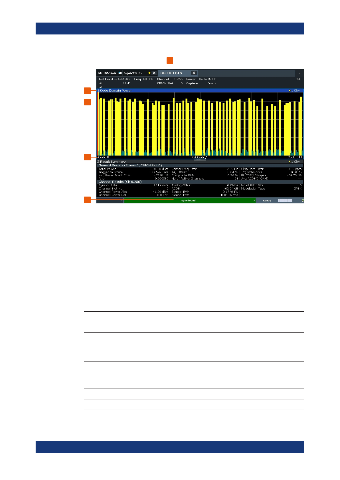
R&S®FSV/A3000-K72/K73
2
3
4
Welcome to the 3GPP FDD applications
Understanding the display information
1
5
1 = Channel bar for firmware and measurement settings
2 = Window title bar with diagram-specific (trace) information
3 = Diagram area
4 = Diagram footer with diagram-specific information
5 = Instrument status bar with error messages, progress bar and date/time display
Channel bar information
In 3GPP FDD applications, when performing Code Domain Analysis, the R&S FSV/A
screen display deviates from the Spectrum application. For RF measurements, the
familiar settings are displayed (see the R&S FSV/A Getting Started manual).
Table 2-1: Hardware settings displayed in the channel bar in 3GPP FDD applications for Code
Ref Level Reference level
Att Mechanical and electronic RF attenuation
Freq Center frequency for the RF signal
Channel Channel number (code number and spreading factor)
CPICH Slot
/ Slot (UE)
Domain Analysis
Slot of the (CPICH) channel
Power Power result mode:
SymbRate Symbol rate of the current channel
Capture (UE application (K73) only): basis for analysis (slot or frame)
●
Absolute
●
Relative to CPICH (BTS application (K72) only)
●
Relative to total power
14User Manual 1178.9461.02 ─ 07

R&S®FSV/A3000-K72/K73
Window title bar information
For each diagram, the header provides the following information:
1 2
Figure 2-1: Window title bar information in 3GPP applications
1 = Window number
2 = Window type
3 = Trace color
4 = Trace number
5 = Detector
Diagram footer information
For most graphical evaluations the diagram footer (beneath the diagram) contains scaling information for the x-axis, where applicable:
Welcome to the 3GPP FDD applications
Understanding the display information
4
3
5
●
Start channel/chip/frame/slot
●
Channel/chip/frame/slot per division
●
Stop channel/chip/frame/slot
For the Bitstream evaluation, the diagram footer indicates:
●
Channel format (type and modulation type (HS-PDSCH only))
●
Number of data bits
●
Number of TPC bits
●
Number of TFCI bits
●
Number of pilot bits
(The bit numbers are indicated in the order they occur.)
Status bar information
Global instrument settings, the instrument status and any irregularities are indicated in
the status bar beneath the diagram. Furthermore, the progress of the current operation
is displayed in the status bar.
15User Manual 1178.9461.02 ─ 07

R&S®FSV/A3000-K72/K73
3 Measurements and result display
The 3GPP FDD applications provide several different measurements for signals
according to the 3GPP FDD standard. The main and default measurement is "Code
Domain Analysis". Furthermore, a "Time Alignment Error" measurement is provided.
In addition to the code domain power measurements specified by the 3GPP standard,
the 3GPP FDD options offer measurements with predefined settings in the frequency
domain, e.g. RF power measurements.
Evaluation methods
The captured and processed data for each measurement can be evaluated with various different methods. All evaluation methods available for the selected 3GPP FDD
measurement are displayed in the evaluation bar in SmartGrid mode.
Evaluation range
You can restrict evaluation to a specific channel, frame or slot, depending on the evaluation method. See Chapter 6.1, "Evaluation range", on page 105.
Measurements and result display
Code domain analysis
● Code domain analysis.............................................................................................16
● Time alignment error measurements...................................................................... 34
● RF measurements...................................................................................................35
3.1 Code domain analysis
Access: [MEAS] > "Code Domain Analyzer"
The "Code Domain Analysis" measurement provides various evaluation methods and
result diagrams.
The code domain power measurements are performed as specified by the 3GPP
standards. A signal section of approximately 20 ms is recorded for analysis and then
searched through to find the start of a 3GPP FDD frame. If a frame start is found in the
signal, the code domain power analysis is performed for a complete frame starting
from slot 0. The different evaluations are calculated from the captured I/Q data set.
Therefore it is not necessary to start a new measurement to change the evaluation.
The 3GPP FDD applications provide the peak code domain error measurement and
composite EVM specified by the 3GPP standard, as well as the code domain power
measurement of assigned and unassigned codes. The power can be displayed either
for all channels in one slot, or for one channel in all slots. The composite constellation
diagram of the entire signal can also be displayed. In addition, the symbols demodulated in a slot, their power, and the determined bits or the symbol EVM can be displayed
for an active channel.
The power of a code channel is always measured in relation to its symbol rate within
the code domain. It can be displayed either as absolute values or relative to the total
signal or the CPICH channel. By default, the power relative to the CPICH channel is
displayed. The total power can vary depending on the slot, since the power can be
16User Manual 1178.9461.02 ─ 07

R&S®FSV/A3000-K72/K73
controlled on a per-slot-basis. The power in the CPICH channel, on the other hand, is
constant in all slots.
For all measurements performed in a slot of a selected channel (bits, symbols, symbol
power, EVM), the actual slot spacing of the channel is taken as a basis, rather than the
CPICH slots. The time reference for the start of a slot is the CPICH slot. If code channels contain a timing offset, the start of a specific slot of the channel differs from the
start of the reference channel (CPICH). Thus, the power-per-channel display is possibly not correct. If channels with a timing offset contain a power control circuit, the channel-power-versus-time display can possibly provide better results.
The composite EVM, peak code domain error and composite constellation measurements are always referenced to the total signal.
Remote command:
CONF:WCDP:MEAS WCDP, see CONFigure:WCDPower[:BTS]:MEASurement
on page 148
Measurements and result display
Code domain analysis
3.1.1 Code domain parameters
Two different types of measurement results are determined and displayed in the
"Result Summary": global results and channel results (for the selected channel).
The number of the CPICH slot at which the measurement is performed is indicated
globally for the measurement in the channel bar.
The spreading code of the selected channel is indicated with the channel number in
the channel bar and above the channel-specific results in the "Result Summary".
In the "Channel Table", the analysis results for all active channels are displayed.
Table 3-1: General code domain power results for a specific frame and slot
Parameter Description
Total Power: The total signal power (average power of total evaluated slot).
Carrier Freq Error: The frequency error relative to the center frequency of the analyzer. The absolute
frequency error is the sum of the analyzer and DUT frequency error. The specified
value is averaged for one (CPICH) slot. See also the note on "Carrier Frequency
Error" on page 18.
Chip Rate Error: The chip rate error in the frame to analyze in ppm. As a result of a high chip rate
error, symbol errors arise and the CDP measurement is possibly not synchronized
to the 3GPP FDD BTS signal. The result is valid even if synchronization of the analyzer and signal failed.
Trigger to Frame: The time difference between the beginning of the recorded signal section to the
start of the analyzed frame. For triggered data collection, this difference is identical
to the time difference of frame trigger (+ trigger offset) – frame start. If synchronization of the analyzer and input signal fails, the value of "Trigger to Frame" is not significant.
IQ Offset: DC offset of the signal in the selected slot in %
IQ Imbalance: I/Q imbalance of signals in the selected slot in %
17User Manual 1178.9461.02 ─ 07

R&S®FSV/A3000-K72/K73
Parameter Description
Measurements and result display
Code domain analysis
Avg Power Inact
Chan
"Composite EVM": The composite EVM is the difference between the test signal and the ideal refer-
Pk CDE (15 ksps): The "Peak Code Domain Error" projects the difference between the test signal and
RHO Quality parameter RHO for each slot.
No of Active Chan: The number of active channels detected in the signal in the selected slot. Both the
Avg. RCDE Average Relative Code Domain Error over all channels detected with 64 QAM (UE:
Average power of the inactive channels
ence signal in the selected slot in %.
See also "Composite EVM" on page 24
the ideal reference signal onto the selected spreading factor in the selected slot
(see "Peak Code Domain Error" on page 28). The spreading factor onto which
projection is performed can be derived from the symbol rate indicated in brackets.
detected data channels and the control channels are considered active channels.
4PAM) modulation in the selected frame.
Carrier Frequency Error
The maximum frequency error that can be compensated is specified in Table 3-2 as a
function of the synchronization mode. Transmitter and receiver should be synchronized
as far as possible.
Table 3-2: Maximum frequency error that can be compensated
SYNC mode ANTENNA DIV Max. Freq. Offset
CPICH X 5.0 kHz
SCH OFF 1.6 kHz
SCH ANT 1 330 Hz
SCH ANT 2 330 Hz
Table 3-3: Channel-specific code domain power results
Symbol Rate: Symbol rate at which the channel is transmitted
Channel Slot No: (BTS measurements only):
Channel slot number; determined by combining the value of the selected CPICH and
the channel's timing offset
Channel Mapping (UE measurements only):
Branch onto which the channel is mapped (I or Q, specified by the standard)
Chan Power Abs: Channel power, absolute
Chan Power Rel: Channel power, relative (referenced to CPICH or total signal power)
Timing Offset: Offset between the start of the first slot in the channel and the start of the analyzed
3GPP FDD BTS frame
RCDE Relative Code Domain Error for the complete frame of the selected channel
"Symbol EVM": Peak and average of the results of the error vector magnitude evaluation
18User Manual 1178.9461.02 ─ 07

R&S®FSV/A3000-K72/K73
No of Pilot Bits: Number of pilot bits of the selected channel
Modulation Type: BTS measurements:
3.1.2 Evaluation methods for code domain analysis
Access: "Overview" > "Display Config"
The captured I/Q data can be evaluated using various different methods without having
to start a new measurement.
The selected evaluation also affects the results of the trace data query (see Chap-
ter 10.9.2, "Measurement results for TRACe<n>[:DATA]? TRACE<n>", on page 223).
Bitstream.......................................................................................................................19
Channel Table............................................................................................................... 20
└ Table Configuration.........................................................................................21
Code Domain Power.....................................................................................................22
Code Domain Error Power............................................................................................23
Composite Constellation............................................................................................... 23
Composite EVM............................................................................................................ 24
EVM vs Chip................................................................................................................. 25
Frequency Error vs Slot................................................................................................ 26
Magnitude Error vs Chip............................................................................................... 26
Marker Table................................................................................................................. 27
Peak Code Domain Error..............................................................................................28
Phase Discontinuity vs Slot...........................................................................................28
Phase Error vs Chip......................................................................................................29
Power vs Slot................................................................................................................ 30
Power vs Symbol.......................................................................................................... 31
Result Summary............................................................................................................31
Symbol Constellation.................................................................................................... 32
Symbol EVM................................................................................................................. 32
Symbol Magnitude Error............................................................................................... 33
Symbol Phase Error......................................................................................................33
Measurements and result display
Code domain analysis
Modulation type of an HSDPA channel. High-speed physical data channels can be
modulated with QPSK, 16 QAM or 64 QAM modulation.
UE measurements: the modulation type of the selected channel. Valid entries are:
●
BPSK I for channels on I-branch
●
BPSK Q for channels on Q-branch
●
NONE for inactive channels
Bitstream
The "Bitstream" evaluation displays the demodulated bits of a selected channel for a
given slot. Depending on the symbol rate, the number of symbols within a slot can vary
from 12 (min) to 384 (max). For QPSK modulation, a symbol consists of 2 bits (I and
Q). For BPSK modulation, a symbol consists of 1 bit (only I used).
19User Manual 1178.9461.02 ─ 07

R&S®FSV/A3000-K72/K73
Figure 3-1: Bitstream display for 3GPP FDD BTS measurements
TIP: Select a specific symbol using the MKR key while the display is focused. If you
enter a number, the marker jumps to the selected symbol, which is highlighted by a
blue circle.
The diagram footer indicates:
●
Channel format (type and modulation type (HS-PDSCH only))
●
Number of data bits (D1 / D2)
●
Number of TPC bits (TPC)
●
Number of TFCI bits (TFCI)
●
Number of pilot bits (Pil)
Remote command:
LAY:ADD? '1',RIGH, BITS, see LAYout:ADD[:WINDow]? on page 207
TRACe<n>[:DATA]? ABITstream
Measurements and result display
Code domain analysis
Channel Table
The "Channel Table" evaluation displays the detected channels and the results of the
code domain power measurement. The channel table can contain a maximum of 512
entries.
In BTS measurements, this number corresponds to the 512 codes that can be
assigned within the class of spreading factor 512.
In UE measurements, this number corresponds to the 256 codes that can be assigned
within the class of spreading factor 256, with both I and Q branches.
The first entries of the table indicate the channels that must be available in the signal to
be analyzed and any other control channels (see Chapter 4.2, "BTS channel types",
on page 44 and Chapter 4.3, "UE channel types", on page 48).
The lower part of the table indicates the data channels that are contained in the signal.
If the type of a channel can be fully recognized, based on pilot sequences or modula-
tion type, the type is indicated in the table. In BTS measurements, all other channels
are of type CHAN.
The channels are in descending order according to symbol rates and, within a symbol
rate, in ascending order according to the channel numbers. Therefore, the unassigned
codes are always displayed at the end of the table.
20User Manual 1178.9461.02 ─ 07

R&S®FSV/A3000-K72/K73
Figure 3-2: Channel Table display for 3GPP FDD BTS measurements
Remote command:
LAY:ADD? '1',RIGH, CTABle, see LAYout:ADD[:WINDow]? on page 207
TRACe<n>[:DATA]? CTABle
TRACe<n>[:DATA]? PWCDp
TRACe<n>[:DATA]? CWCDp
Table Configuration ← Channel Table
You can configure which parameters are displayed in the "Channel Table" by clicking
(not double-clicking!) a column header.
A "Table Configuration" dialog box is displayed in which you can select the columns to
be displayed.
Measurements and result display
Code domain analysis
By default, only active channels are displayed. To display all channels, including the
inactive ones, enable the "Show Inactive Channels" option.
The following parameters of the detected channels are determined by the CDP measurement and can be displayed in the "Channel Table" evaluation. (For details see
Chapter 3.1.1, "Code domain parameters", on page 17.)
21User Manual 1178.9461.02 ─ 07

R&S®FSV/A3000-K72/K73
Table 3-4: Code domain power results in the channel table
Label Description
Chan Type Type of channel (active channels only)
Ch. SF Number of channel spreading code (0 to [spreading factor-1])
Symbol Rate [ksps] Symbol rate at which the channel is transmitted
State Active: channel is active and all pilot symbols are correct
TFCI (BTS measurements only):
Mapping (UE measurements only):
PilotL [Bits] Number of pilot bits in the channel
Measurements and result display
Code domain analysis
In BTS measurements: always
Inactive: channel is not active
Pilotf: channel is active, but pilot symbols incomplete or missing
Data channel uses TFCI symbols
Branch the channel is mapped to (I or Q)
(UE measurements: only for control channel DPCCH)
Pwr Abs [dBm]/Pwr Rel [dBm] Absolute and relative channel power (referred to the CPICH or the
total power of the signal)
T Offs [Chips] (BTS measurements only):
Timing offset
Code Domain Power
Figure 3-3: Code Domain Power Display for 3GPP FDD BTS measurements
The "Code Domain Power" evaluation shows the power of all possible code channels
in the selected channel slot. The x-axis shows the possible code channels from 0 to
the highest spreading factor. Due to the circumstance that the power is regulated from
slot to slot, the result power can differ between different slots. Detected channels are
displayed yellow. The selected code channel is highlighted red. The codes where no
channel could be detected are displayed green.
Note: Effects of missing or incomplete pilot symbols. In "Autosearch" channel detection
mode, the application expects specific pilot symbols for DPCH channels. If these symbols are missing or incomplete, the channel power in the "Code Domain Power" evaluation is displayed green at the points of the diagram the channel should appear due to
its spreading code. Furthermore, a message ("INCORRECT PILOT") is displayed in
22User Manual 1178.9461.02 ─ 07

R&S®FSV/A3000-K72/K73
the status bar. In this case, check the pilot symbols for those channels using the
"Power vs Slot" or the "Bitstream" evaluations.
Optionally, all QPSK-modulated channels can also be recognized without pilot symbols
(see "HSDPA/UPA" on page 61).
Remote command:
LAY:ADD? '1',RIGH, CDPower, see LAYout:ADD[:WINDow]? on page 207
CALC:MARK:FUNC:WCDP:RES? CDP, seeCALCulate<n>:MARKer<m>:FUNCtion:
WCDPower[:BTS]:RESult on page 221
CALC:MARK:FUNC:WCDP:MS:RES? CDP, see CALCulate<n>:MARKer<m>:
FUNCtion:WCDPower:MS:RESult? on page 220
TRACe<n>[:DATA]? CTABle
TRACe<n>[:DATA]? PWCDp
TRACe<n>[:DATA]? CWCDp
Code Domain Error Power
"Code Domain Error Power" is the difference in power between the measured and the
ideal signal. The unit is dB. There are no other units for the y-axis.
Measurements and result display
Code domain analysis
Figure 3-4: Code Domain Error Power Display for 3GPP FDD BTS measurements
Remote command:
LAY:ADD? '1',RIGH, CDEPower, see LAYout:ADD[:WINDow]? on page 207
TRACe<n>[:DATA]? TRACE<1...4>
Composite Constellation
The "Composite Constellation" evaluation analyzes the entire signal for one single slot.
If many channels are to be analyzed, the results are superimposed. In that case, the
benefit of this evaluation is limited (senseless).
In "Composite Constellation" evaluation the constellation points of the 1536 chips are
displayed for the specified slot. This data is determined inside the DSP even before the
channel search. Thus, it is not possible to assign constellation points to channels. The
constellation points are displayed normalized to the total power.
23User Manual 1178.9461.02 ─ 07

R&S®FSV/A3000-K72/K73
2560|%100*
²
²
1
0
0
N
x
xs
EVM
N
n
n
N
n
nn
RMS
Figure 3-5: Composite Constellation display for 3GPP FDD BTS measurements
Remote command:
LAY:ADD? '1',RIGH, CCONst, see LAYout:ADD[:WINDow]? on page 207
TRACe<n>[:DATA]? TRACE<1...4>
Composite EVM
The "Composite EVM" evaluation displays the root mean square composite EVM
(modulation accuracy) according to the 3GPP specification. The square root is determined of the mean squared errors between the real and imaginary components of the
received signal, and an ideal reference signal (EVM referenced to the total signal). The
error is averaged over all channels for individual slots. The "Composite EVM" evaluation covers the entire signal during the entire observation time.
Measurements and result display
Code domain analysis
where:
EVM
RMS
s
n
x
n
n index number for mean power calculation of received and reference signal.
N number of chips at each CPICH slot
root mean square of the vector error of the composite signal
complex chip value of received signal
complex chip value of reference signal
24User Manual 1178.9461.02 ─ 07

R&S®FSV/A3000-K72/K73
Figure 3-6: Composite EVM display for 3GPP FDD BTS measurements
The measurement result consists of one composite EVM measurement value per slot.
In this case, the measurement interval is the slot spacing of the CPICH (timing offset of
0 chips referenced to the beginning of the frame). Only the channels recognized as
active are used to generate the ideal reference signal. If an assigned channel is not
recognized as active because pilot symbols are missing or incomplete, the difference
between the measurement and reference signal and the composite EVM is very high.
Remote command:
LAY:ADD? '1',RIGH, CEVM, see LAYout:ADD[:WINDow]? on page 207
TRACe<n>[:DATA]? TRACE<1...4>
Measurements and result display
Code domain analysis
EVM vs Chip
"EVM vs Chip" activates the Error Vector Magnitude (EVM) versus chip display. The
EVM is displayed for all chips of the selected slot.
Note: In UE measurements, if the measurement interval "Halfslot" is selected for evaluation, 30 slots are displayed instead of the usual 15 (see "Measurement Interval"
on page 109).
The EVM is calculated by the root of the square difference of received signal and reference signal. The reference signal is estimated from the channel configuration of all
active channels. The EVM is related to the square root of the mean power of reference
signal and given in percent.
where:
EVM
s
k
x
k
k
vector error of the chip EVM of chip number k
complex chip value of received signal
complex chip value of reference signal
k index number of the evaluated chip
25User Manual 1178.9461.02 ─ 07

R&S®FSV/A3000-K72/K73
N number of chips at each CPICH slot
n index number for mean power calculation of reference signal
Figure 3-7: EVM vs Chip display for 3GPP FDD BTS measurements
Remote command:
LAY:ADD? '1',RIGH, EVMChip, see LAYout:ADD[:WINDow]? on page 207
TRACe<n>[:DATA]? TRACE<1...4>
Measurements and result display
Code domain analysis
Frequency Error vs Slot
For each value to be displayed, the difference between the frequency error of the corresponding slot to the frequency error of the first (zero) slot is calculated (based on
CPICH slots). This helps eliminate a static frequency offset of the whole signal to achieve a better display of the actual time-dependant frequency diagram.
Figure 3-8: Frequency Error vs Slot display for 3GPP FDD BTS measurements
Remote command:
LAY:ADD? '1',RIGH, FESLot, see LAYout:ADD[:WINDow]? on page 207
TRACe<n>[:DATA]? ATRACE
Magnitude Error vs Chip
The Magnitude Error versus chip display shows the magnitude error for all chips of the
selected slot.
Note: In UE measurements, if the measurement interval "Halfslot" is selected for evaluation, 30 slots are displayed instead of the usual 15 (see "Measurement Interval"
on page 109).
26User Manual 1178.9461.02 ─ 07

R&S®FSV/A3000-K72/K73
The magnitude error is calculated as the difference of the magnitude of the received
signal to the magnitude of the reference signal. The reference signal is estimated from
the channel configuration of all active channels. The magnitude error is related to the
square root of the mean power of reference signal and given in percent.
Where:
Measurements and result display
Code domain analysis
MAG
k
s
k
x
k
k Index number of the evaluated chip
N Number of chips at each CPICH slot
n Index number for mean power calculation of reference signal
Figure 3-9: Magnitude Error vs Chip display for 3GPP FDD BTS measurements
Magnitude error of chip number k
Complex chip value of received signal
Complex chip value of reference signal
Remote command:
LAY:ADD? '1',RIGH, MECHip, see LAYout:ADD[:WINDow]? on page 207
TRACe<n>[:DATA]? TRACE<1...4>
Marker Table
Displays a table with the current marker values for the active markers.
This table is displayed automatically if configured accordingly.
Tip: To navigate within long marker tables, simply scroll through the entries with your
finger on the touchscreen.
27User Manual 1178.9461.02 ─ 07

R&S®FSV/A3000-K72/K73
Remote command:
LAY:ADD? '1',RIGH, MTAB, see LAYout:ADD[:WINDow]? on page 207
Results:
CALCulate<n>:MARKer<m>:X on page 247
CALCulate<n>:MARKer<m>:Y? on page 248
Peak Code Domain Error
In line with the 3GPP specifications, the error between the measurement signal and
the ideal reference signal for a given slot and for all codes is projected onto the various
spreading factors. The result consists of the peak code domain error value per slot.
The measurement interval is the slot spacing of the CPICH (timing offset of 0 chips referenced to the beginning of the frame). Only the channels recognized as active are
used to generate the ideal reference signal for the peak code domain error. If an
assigned channel is not recognized as active since pilot symbols are missing or incomplete, the difference between the measurement and reference signal is very high. This
display is a bar diagram over slots. The unit is dB. The "Peak Code Domain Error"
evaluation covers the entire signal and the entire observation time.
Measurements and result display
Code domain analysis
Figure 3-10: Peak Code Domain Error display for 3GPP FDD BTS measurements
Remote command:
LAY:ADD? '1',RIGH, PCDerror, see LAYout:ADD[:WINDow]? on page 207
TRACe<n>[:DATA]? TRACE<1...4>
Phase Discontinuity vs Slot
The "Phase Discontinuity vs Slot" is calculated according to 3GPP specifications. The
phase calculated for each slot is interpolated to both ends of the slot using the frequency shift of that slot. The difference between the phase interpolated for the beginning of one slot and the end of the preceding slot is displayed as the phase discontinuity of that slot.
28User Manual 1178.9461.02 ─ 07

R&S®FSV/A3000-K72/K73
Figure 3-11: Phase Discontinuity vs Slot display for 3GPP FDD BTS measurements
Remote command:
LAY:ADD? '1',RIGH, PDSLot, see LAYout:ADD[:WINDow]? on page 207
TRACe<n>[:DATA]? TRACE<1...4>
Phase Error vs Chip
"Phase Error vs Chip" activates the phase error versus chip display. The phase error is
displayed for all chips of the selected slot.
Note: In UE measurements, if the measurement interval "Halfslot" is selected for evaluation, 30 slots are displayed instead of the usual 15 (see "Measurement Interval"
on page 109).
The phase error is calculated by the difference of the phase of received signal and
phase of reference signal. The reference signal is estimated from the channel configuration of all active channels. The phase error is given in degrees in a range of +180° to
-180°.
Measurements and result display
Code domain analysis
Figure 3-12: Calculating the magnitude, phase and vector error per chip
Where:
29User Manual 1178.9461.02 ─ 07

R&S®FSV/A3000-K72/K73
Measurements and result display
Code domain analysis
PHI
k
s
k
x
k
k Index number of the evaluated chip
N Number of chips at each CPICH slot
φ(x) Phase calculation of a complex value
Phase error of chip number k
Complex chip value of received signal
Complex chip value of reference signal
Remote command:
LAY:ADD? '1',RIGH, PECHip, see LAYout:ADD[:WINDow]? on page 207
TRACe<n>[:DATA]? TRACE<1...4>
Power vs Slot
The "Power vs Slot" evaluation displays the power of the selected channel for each
slot. The power is displayed either absolute or relative to the total power of the signal
or to the CPICH channel.
Note: In UE measurements, this evaluation is only available if the analysis mode
"Frame" is selected (see "Capture Mode" on page 82).
If the measurement interval "Halfslot" is selected for evaluation, 30 slots are displayed
instead of the usual 15 (see "Measurement Interval" on page 109).
Figure 3-13: Power vs Slot Display for 3GPP FDD BTS measurements
30User Manual 1178.9461.02 ─ 07
 Loading...