

R&S®FPS-K72/K73
3GPP FDD Measurements Options
User Manual
(;ÚãF2)
1176.8522.02 ─ 08
User Manual
Test & Measurement

This manual applies to the following R&S®FPS models with firmware version 1.50 and higher:
●
R&S®FPS4 (1319.2008K04)
●
R&S®FPS7 (1319.2008K07)
●
R&S®FPS13 (1319.2008K13)
●
R&S®FPS30 (1319.2008K30)
●
R&S®FPS40 (1319.2008K40)
The following firmware options are described:
●
R&S FPS-K72 (1321.4133.02)
●
R&S FPS-K73 (1321.4140.02)
The software contained in this product uses several valuable open source software packages. For information, see the "Open
Source Acknowledgment" on the user documentation CD-ROM (included in delivery).
Rohde & Schwarz would like to thank the open source community for their valuable contribution to embedded computing.
© 2017 Rohde & Schwarz GmbH & Co. KG
Mühldorfstr. 15, 81671 München, Germany
Phone: +49 89 41 29 - 0
Fax: +49 89 41 29 12 164
Email: info@rohde-schwarz.com
Internet: www.rohde-schwarz.com
Subject to change – Data without tolerance limits is not binding.
R&S® is a registered trademark of Rohde & Schwarz GmbH & Co. KG.
Trade names are trademarks of their owners.
The following abbreviations are used throughout this manual: R&S®FPS is abbreviated as R&S FPS. "R&S FPS-K72 and R&S FPSK73" are abbreviated as "R&S FPS-K72/K73".

R&S®FPS-K72/K73
Contents
1 Preface.................................................................................................... 7
1.1 About this Manual......................................................................................................... 7
1.2 Typographical Conventions.........................................................................................8
2 Welcome to the 3GPP FDD Applications............................................. 9
2.1 Starting the 3GPP FDD Application.............................................................................9
2.2 Understanding the Display Information....................................................................11
3 Measurements and Result Display.....................................................13
3.1 Code Domain Analysis............................................................................................... 13
3.2 Time Alignment Error Measurements....................................................................... 31
3.3 RF Measurements....................................................................................................... 33
Contents
4 Measurement Basics........................................................................... 40
4.1 Channel Detection.......................................................................................................43
4.2 BTS Channel Types.................................................................................................... 43
4.3 UE Channel Types.......................................................................................................47
4.4 3GPP FDD BTS Test Models...................................................................................... 48
4.5 Setup for Base Station Tests..................................................................................... 49
4.6 3GPP FDD UE Test Models........................................................................................ 50
4.7 Setup for User Equipment Tests............................................................................... 51
4.8 Time Alignment Error Measurements....................................................................... 52
4.9 CDA Measurements in MSRA Operating Mode........................................................ 54
5 Configuration........................................................................................56
5.1 Result Display............................................................................................................. 56
5.2 Code Domain Analysis............................................................................................... 57
5.3 Time Alignment Error Measurements....................................................................... 92
5.4 RF Measurements....................................................................................................... 99
6 Analysis.............................................................................................. 104
6.1 Evaluation Range...................................................................................................... 104
6.2 Code Domain Settings (BTS Measurements)......................................................... 107
6.3 Code Domain Settings (UE Measurements)........................................................... 109
6.4 Traces.........................................................................................................................110
3User Manual 1176.8522.02 ─ 08

R&S®FPS-K72/K73
6.5 Trace / Data Export Configuration...........................................................................112
6.6 Markers...................................................................................................................... 113
7 I/Q Data Import and Export................................................................120
7.1 Import/Export Functions.......................................................................................... 120
8 Optimizing and Troubleshooting the Measurement....................... 123
8.1 Error Messages......................................................................................................... 123
9 How to Perform Measurements in 3GPP FDD Applications.......... 124
10 Measurement Examples.................................................................... 129
10.1 Measurement 1: Measuring the Signal Channel Power.........................................129
10.2 Measurement 2: Determining the Spectrum Emission Mask................................130
10.3 Measurement 3: Measuring the Relative Code Domain Power.............................132
Contents
10.4 Measurement 4: Triggered Measurement of Relative Code Domain Power........136
10.5 Measurement 5: Measuring the Composite EVM................................................... 138
10.6 Measurement 6: Determining the Peak Code Domain Error................................. 139
11 Remote Commands for 3GPP FDD Measurements........................ 142
11.1 Introduction............................................................................................................... 142
11.2 Common Suffixes......................................................................................................147
11.3 Activating 3GPP FDD Measurements......................................................................148
11.4 Selecting a Measurement......................................................................................... 152
11.5 Configuring Code Domain Analysis and Time Alignment Error Measurements
.................................................................................................................................... 153
11.6 Configuring RF Measurements................................................................................205
11.7 Configuring the Result Display................................................................................207
11.8 Starting a Measurement........................................................................................... 215
11.9 Retrieving Results.....................................................................................................220
11.10 Analysis..................................................................................................................... 247
11.11 Importing and Exporting I/Q Data and Results...................................................... 259
11.12 Configuring the Slave Application Data Range (MSRA mode only).....................261
11.13 Querying the Status Registers.................................................................................263
11.14 Deprecated Commands............................................................................................ 266
11.15 Programming Examples (R&S FPS-k72).................................................................269
12 I/Q Data File Format (iq-tar)...............................................................277
4User Manual 1176.8522.02 ─ 08

R&S®FPS-K72/K73
12.1 I/Q Parameter XML File Specification......................................................................278
12.2 I/Q Data Binary File................................................................................................... 281
List of Remote Commands (3GPP FDD).......................................... 283
Index....................................................................................................288
Contents
5User Manual 1176.8522.02 ─ 08

R&S®FPS-K72/K73
Contents
6User Manual 1176.8522.02 ─ 08

R&S®FPS-K72/K73
1 Preface
Preface
About this Manual
1.1 About this Manual
This 3GPP FDD User Manual provides all the information specific to the 3GPP FDD
applications. All general instrument functions and settings common to all applications
and operating modes are described in the main R&S FPS User Manual.
The main focus in this manual is on the measurement results and the tasks required to
obtain them. The following topics are included:
●
Welcome to the 3GPP FDD Measurements Application
Introduction to and getting familiar with the application
●
Measurements and Result Displays
Details on supported measurements and their result types
●
Measurement Basics
Background information on basic terms and principles in the context of the measurement
●
Configuration + Analysis
A concise description of all functions and settings available to configure measurements and analyze results with their corresponding remote control command
●
I/Q Data Import and Export
Description of general functions to import and export raw I/Q (measurement) data
●
Optimizing and Troubleshooting the Measurement
Hints and tips on how to handle errors and optimize the test setup
●
How to Perform Measurements in 3GPP FDD Applications
The basic procedure to perform each measurement and step-by-step instructions
for more complex tasks or alternative methods
●
Measurement Examples
Detailed measurement examples to guide you through typical measurement scenarios and allow you to try out the application immediately
●
Remote Commands for 3GPP FDD Measurements
Remote commands required to configure and perform 3GPP FDD measurements
in a remote environment, sorted by tasks
(Commands required to set up the environment or to perform common tasks on the
instrument are provided in the main R&S FPS User Manual)
Programming examples demonstrate the use of many commands and can usually
be executed directly for test purposes
●
List of remote commands
Alpahabetical list of all remote commands described in the manual
●
Index
7User Manual 1176.8522.02 ─ 08
R&S®FPS-K72/K73
Preface
Typographical Conventions
1.2 Typographical Conventions
The following text markers are used throughout this documentation:
Convention Description
"Graphical user interface elements"
KEYS Key names are written in capital letters.
File names, commands,
program code
Input Input to be entered by the user is displayed in italics.
Links Links that you can click are displayed in blue font.
"References" References to other parts of the documentation are enclosed by quota-
All names of graphical user interface elements on the screen, such as
dialog boxes, menus, options, buttons, and softkeys are enclosed by
quotation marks.
File names, commands, coding samples and screen output are distinguished by their font.
tion marks.
8User Manual 1176.8522.02 ─ 08

R&S®FPS-K72/K73
2 Welcome to the 3GPP FDD Applications
The 3GPP FDD applications add functionality to the R&S FPS to perform code domain
analysis or power measurements according to the 3GPP standard (FDD mode). The
application firmware is in line with the 3GPP standard (Third Generation Partnership
Project) with Release 5. Signals that meet the conditions for channel configuration of
test models 1 to 4 according to the 3GPP standard, e.g. W-CDMA signals using FDD,
can be measured with the 3GPP FDD BTS application. In addition to the code domain
measurements specified by the 3GPP standard, the application firmware offers measurements with predefined settings in the frequency domain, e.g. power and ACLR
measurements.
R&S FPS-K72 performs Base Transceiver Station (BTS) measurements (for downlink
signals).
R&S FPS-K73 performs User Equipment (UE) measurements (for uplink signals).
In particular, the 3GPP FDD applications feature:
●
●
●
●
●
Welcome to the 3GPP FDD Applications
Starting the 3GPP FDD Application
Code domain analysis, providing results like code domain power, EVM, peak code
domain error etc.
Time alignment error determination
Various power measurements
Spectrum Emission Mask measurements
Statistical (CCDF) evaluation
This user manual contains a description of the functionality that the application provides, including remote control operation.
Functions that are not discussed in this manual are the same as in the Spectrum application and are described in the R&S FPS User Manual. The latest version is available
for download at the product homepage
http://www2.rohde-schwarz.com/product/FPS.html.
Installation
You can find detailed installation instructions in the R&S FPS Getting Started manual
or in the Release Notes.
2.1 Starting the 3GPP FDD Application
The 3GPP FDD measurements require a special application on the R&S FPS.
9User Manual 1176.8522.02 ─ 08
R&S®FPS-K72/K73
Manual operation via an external monitor and mouse
Although the R&S FPS does not have a built-in display, it is possible to operate it interactively in manual mode using a graphical user interface with an external monitor and
a mouse connected.
It is recommended that you use the manual mode initially to get familiar with the instrument and its functions before using it in pure remote mode. Thus, this document
describes in detail how to operate the instrument manually using an external monitor
and mouse. The remote commands are described in the second part of the document.
For details on manual operation see the R&S FPS Getting Started manual.
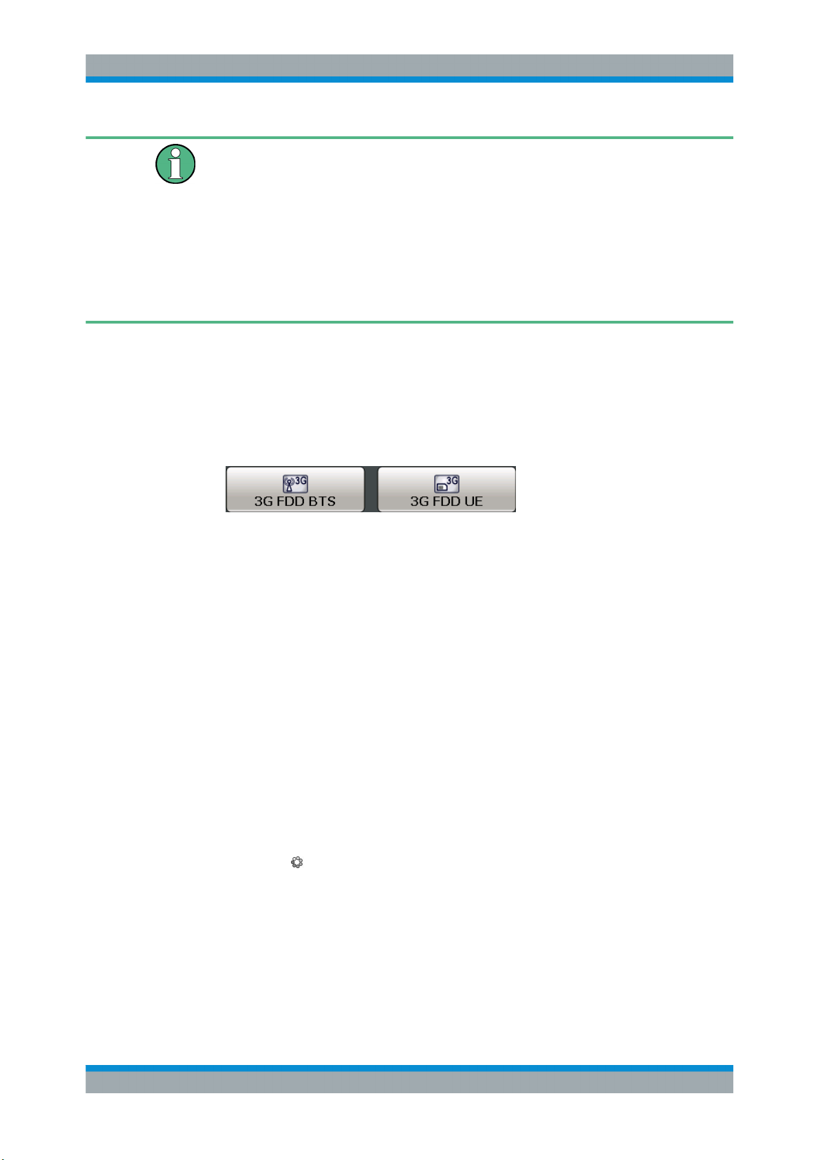
To activate the 3GPP FDD applications
1. Select the MODE key.
2. Select the "3GPP FDD BTS" or "3GPP FDD UE" item.
Welcome to the 3GPP FDD Applications
Starting the 3GPP FDD Application
A dialog box opens that contains all operating modes and applications currently
available on your R&S FPS.
The R&S FPS opens a new measurement channel for the 3GPP FDD application.
A Code Domain Analysis measurement is started immediately with the default settings.
It can be configured in the 3GPP FDD "Overview" dialog box, which is displayed when
you select the "Overview" softkey from any menu (see Chapter 5.2.1, "Configuration
Overview", on page 58).
Multiple Measurement Channels and Sequencer Function
When you activate an application, a new measurement channel is created which determines the measurement settings for that application. The same application can be activated with different measurement settings by creating several channels for the same
application.
Only one measurement can be performed at any time, namely the one in the currently
active channel. However, in order to perform the configured measurements consecutively, a Sequencer function is provided.
If activated, the measurements configured in the currently active channels are performed one after the other in the order of the tabs. The currently active measurement is
indicated by a
are updated in the tabs (including the "MultiView") as the measurements are performed. Sequential operation itself is independent of the currently displayed tab.
For details on the Sequencer function see the R&S FPS User Manual.
symbol in the tab label. The result displays of the individual channels
10User Manual 1176.8522.02 ─ 08
R&S®FPS-K72/K73
Welcome to the 3GPP FDD Applications
Understanding the Display Information
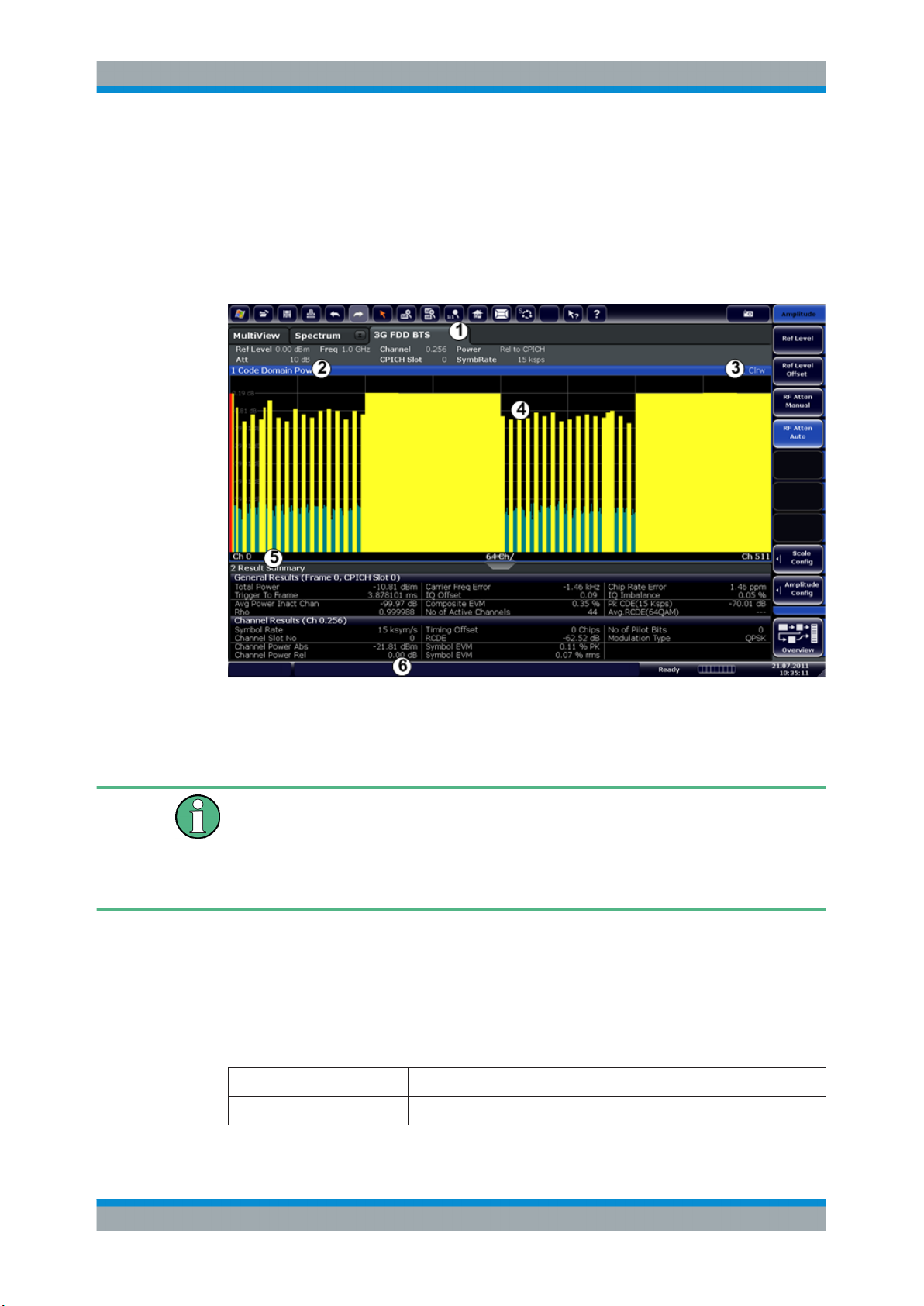
2.2 Understanding the Display Information
The following figure shows a measurement diagram during a 3GPP FDD BTS measurement. All different information areas are labeled. They are explained in more detail
in the following sections.
(The basic screen elements are identical for 3GPP FDD UE measurements)
1
= Channel bar for firmware and measurement settings
2+3 = Window title bar with diagram-specific (trace) information
4 = Diagram area
5 = Diagram footer with diagram-specific information
6 = Instrument status bar with error messages, progress bar and date/time display
MSRA operating mode
In MSRA operating mode, additional tabs and elements are available. A colored background of the screen behind the measurement channel tabs indicates that you are in
MSRA operating mode.
For details on the MSRA operating mode see the R&S FPS MSRA User Manual.
Channel bar information
In 3GPP FDD applications, when performing Code Domain Analysis, the R&S FPS
screen display deviates from the Spectrum application. For RF measurements, the
familiar settings are displayed (see the R&S FPS Getting Started manual).
Table 2-1: Hardware settings displayed in the channel bar in 3GPP FDD applications for Code
Ref Level Reference level
Att Mechanical and electronic RF attenuation
Domain Analysis
11User Manual 1176.8522.02 ─ 08

R&S®FPS-K72/K73
Welcome to the 3GPP FDD Applications
Understanding the Display Information
Freq Center frequency for the RF signal
Channel Channel number (code number and spreading factor)
CPICH Slot
/ Slot (UE)
Power Power result mode:
SymbRate Symbol rate of the current channel
Capture (UE application (K73) only): basis for analysis (slot or frame)
Slot of the (CPICH) channel
●
Absolute
●
Relative to CPICH (BTS application (K72) only)
●
Relative to total power
Window title bar information
For each diagram, the header provides the following information:
Figure 2-1: Window title bar information in 3GPP applications
1 = Window number
2 = Window type
3 = Trace color
4 = Trace number
5 = Detector
Diagram footer information
For most graphical evaluations the diagram footer (beneath the diagram) contains scaling information for the x-axis, where applicable:
●
Start channel/chip/frame/slot
●
Channel/chip/frame/slot per division
●
Stop channel/chip/frame/slot
For the Bitstream evaluation, the diagram footer indicates:
●
Channel format (type and modulation type (HS-PDSCH only))
●
Number of data bits
●
Number of TPC bits
●
Number of TFCI bits
●
Number of pilot bits
(The bit numbers are indicated in the order they occur.)
Status bar information
Global instrument settings, the instrument status and any irregularities are indicated in
the status bar beneath the diagram. Furthermore, the progress of the current operation
is displayed in the status bar.
12User Manual 1176.8522.02 ─ 08

R&S®FPS-K72/K73
3 Measurements and Result Display
The 3GPP FDD applications provide several different measurements for signals
according to the 3GPP FDD standard. The main and default measurement is Code
Domain Analysis. Furthermore, a Time Alignment Error measurement is provided.
In addition to the code domain power measurements specified by the 3GPP standard,
the 3GPP FDD options offer measurements with predefined settings in the frequency
domain, e.g. RF power measurements.
Evaluation methods
The captured and processed data for each measurement can be evaluated with various different methods. All evaluation methods available for the selected 3GPP FDD
measurement are displayed in the evaluation bar in SmartGrid mode.
Evaluation range
You can restrict evaluation to a specific channel, frame or slot, depending on the evaluation method. See Chapter 6.1, "Evaluation Range", on page 104.
Measurements and Result Display
Code Domain Analysis
● Code Domain Analysis............................................................................................13
● Time Alignment Error Measurements..................................................................... 31
● RF Measurements...................................................................................................33
3.1 Code Domain Analysis
Access: MEAS > "Code Domain Analyzer"
The Code Domain Analysis measurement provides various evaluation methods and
result diagrams.
The code domain power measurements are performed as specified by the 3GPP
standards. A signal section of approximately 20 ms is recorded for analysis and then
searched through to find the start of a 3GPP FDD frame. If a frame start is found in the
signal, the code domain power analysis is performed for a complete frame starting
from slot 0. The different evaluations are calculated from the captured I/Q data set.
Therefore it is not necessary to start a new measurement in order to change the evaluation.
The 3GPP FDD applications provide the peak code domain error measurement and
composite EVM specified by the 3GPP standard, as well as the code domain power
measurement of assigned and unassigned codes. The power can be displayed either
for all channels in one slot, or for one channel in all slots. The composite constellation
diagram of the entire signal can also be displayed. In addition, the symbols demodulated in a slot, their power, and the determined bits or the symbol EVM can be displayed
for an active channel.
The power of a code channel is always measured in relation to its symbol rate within
the code domain. It can be displayed either as absolute values or relative to the total
signal or the CPICH channel. By default, the power relative to the CPICH channel is
13User Manual 1176.8522.02 ─ 08

R&S®FPS-K72/K73
displayed. The total power may vary depending on the slot, since the power can be
controlled on a per-slot-basis. The power in the CPICH channel, on the other hand, is
constant in all slots.
For all measurements performed in a slot of a selected channel (bits, symbols, symbol
power, EVM), the actual slot spacing of the channel is taken as a basis, rather than the
CPICH slots. The time reference for the start of a slot is the CPICH slot. If code channels contain a timing offset, the start of a specific slot of the channel differs from the
start of the reference channel (CPICH). Thus, the power-per-channel display may not
be correct. If channels with a timing offset contain a power control circuit, the channelpower-versus-time display may provide better results.
The composite EVM, peak code domain error and composite constellation measurements are always referenced to the total signal.
Remote command:
CONF:WCDP:MEAS WCDP, see CONFigure:WCDPower[:BTS]:MEASurement
on page 152
Measurements and Result Display
Code Domain Analysis
3.1.1 Code Domain Parameters
Two different types of measurement results are determined and displayed in the Result
Summary: global results and channel results (for the selected channel).
The number of the CPICH slot at which the measurement is performed is indicated
globally for the measurement in the channel bar.
The spreading code of the selected channel is indicated with the channel number in
the channel bar and above the channel-specific results in the Result Summary.
In the Channel Table, the analysis results for all active channels are displayed.
Table 3-1: General code domain power results for a specific frame and slot
Parameter Description
Total Power: The total signal power (average power of total evaluated slot).
Carrier Freq Error: The frequency error relative to the center frequency of the analyzer. The absolute
frequency error is the sum of the analyzer and DUT frequency error. The specified
value is averaged for one (CPICH) slot. See also the note on "Carrier Frequency
Error" on page 15.
Chip Rate Error: The chip rate error in the frame to analyze in ppm. As a result of a high chip rate
error, symbol errors arise and the CDP measurement is possibly not synchronized
to the 3GPP FDD BTS signal. The result is valid even if synchronization of the analyzer and signal failed.
Trigger to Frame: The time difference between the beginning of the recorded signal section to the
start of the analyzed frame. In case of triggered data collection, this difference is
identical with the time difference of frame trigger (+ trigger offset) – frame start. If
synchronization of the analyzer and input signal fails, the value of "Trigger to
Frame" is not significant.
IQ Offset: DC offset of the signal in the selected slot in %
14User Manual 1176.8522.02 ─ 08
R&S®FPS-K72/K73
Measurements and Result Display
Code Domain Analysis
Parameter Description
IQ Imbalance: I/Q imbalance of signals in the selected slot in %
Avg Power Inact
Chan
Composite EVM: The composite EVM is the difference between the test signal and the ideal refer-
Pk CDE (15 ksps): The Peak Code Domain Error projects the difference between the test signal and
RHO Quality parameter RHO for each slot.
No of Active Chan: The number of active channels detected in the signal in the selected slot. Both the
Avg. RCDE Average Relative Code Domain Error over all channels detected with 64 QAM (UE:
Average power of the inactive channels
ence signal in the selected slot in %.
See also "Composite EVM" on page 21
the ideal reference signal onto the selected spreading factor in the selected slot
(see "Peak Code Domain Error" on page 25). The spreading factor onto which
projection is performed can be derived from the symbol rate indicated in brackets.
detected data channels and the control channels are considered active channels.
4PAM) modulation in the selected frame.
Carrier Frequency Error
The maximum frequency error that can be compensated is specified in Table 3-2 as a
function of the synchronization mode. Transmitter and receiver should be synchronized
as far as possible.
Table 3-2: Maximum frequency error that can be compensated
SYNC mode ANTENNA DIV Max. Freq. Offset
CPICH X 5.0 kHz
SCH OFF 1.6 kHz
SCH ANT 1 330 Hz
SCH ANT 2 330 Hz
Table 3-3: Channel-specific code domain power results
Symbol Rate: Symbol rate at which the channel is transmitted
Channel Slot No: (BTS measurements only):
Channel slot number; determined by combining the value of the selected CPICH and
the channel's timing offset
Channel Mapping (UE measurements only):
Branch onto which the channel is mapped (I or Q, specified by the standard)
Chan Power Abs: Channel power, absolute
Chan Power Rel: Channel power, relative (referenced to CPICH or total signal power)
Timing Offset: Offset between the start of the first slot in the channel and the start of the analyzed
3GPP FDD BTS frame
RCDE Relative Code Domain Error for the complete frame of the selected channel
15User Manual 1176.8522.02 ─ 08

R&S®FPS-K72/K73
Measurements and Result Display
Code Domain Analysis
Symbol EVM: Peak and average of the results of the error vector magnitude evaluation
No of Pilot Bits: Number of pilot bits of the selected channel
Modulation Type: BTS measurements:
Modulation type of an HSDPA channel. High speed physical data channels can be
modulated with QPSK, 16 QAM or 64 QAM modulation.
UE measurements: the modulation type of the selected channel. Valid entries are:
●
BPSK I for channels on I-branch
●
BPSK Q for channels on Q-branch
●
NONE for inactive channels
3.1.2 Evaluation Methods for Code Domain Analysis
Access: "Overview" > "Display Config"
The captured I/Q data can be evaluated using various different methods without having
to start a new measurement.
The selected evaluation also affects the results of the trace data query (see Chap-
ter 11.9.2, "Measurement Results for TRACe<n>[:DATA]? TRACE<n>", on page 225).
Bitstream.......................................................................................................................16
Channel Table...............................................................................................................17
└ Table Configuration.........................................................................................18
Code Domain Power.....................................................................................................19
Code Domain Error Power............................................................................................20
Composite Constellation............................................................................................... 20
Composite EVM............................................................................................................ 21
EVM vs Chip................................................................................................................. 22
Frequency Error vs Slot................................................................................................ 23
Mag Error vs Chip......................................................................................................... 23
Marker Table ................................................................................................................24
Peak Code Domain Error..............................................................................................25
Phase Discontinuity vs Slot...........................................................................................25
Phase Error vs Chip......................................................................................................26
Power vs Slot................................................................................................................ 27
Power vs Symbol.......................................................................................................... 28
Result Summary............................................................................................................28
Symbol Constellation.................................................................................................... 29
Symbol EVM................................................................................................................. 29
Symbol Magnitude Error............................................................................................... 30
Symbol Phase Error......................................................................................................30
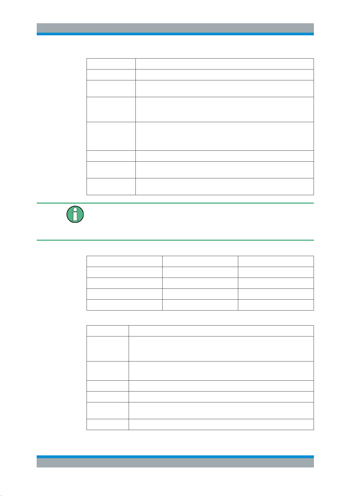
Bitstream
The Bitstream evaluation displays the demodulated bits of a selected channel for a
given slot. Depending on the symbol rate the number of symbols within a slot can vary
from 12 (min) to 384 (max). For QPSK modulation a symbol consists of 2 bits (I and
Q). For BPSK modulation a symbol consists of 1 bit (only I used).
16User Manual 1176.8522.02 ─ 08
R&S®FPS-K72/K73
Figure 3-1: Bitstream display for 3GPP FDD BTS measurements
TIP: Select a specific symbol using the MKR key while the display is focused. If you
enter a number, the marker jumps to the selected symbol, which is highlighted by a
blue circle.
The diagram footer indicates:
●
●
●
●
●
Remote command:
LAY:ADD? '1',RIGH, BITS, see LAYout:ADD[:WINDow]? on page 208
TRACe<n>[:DATA]? ABITstream
Measurements and Result Display
Code Domain Analysis
Channel format (type and modulation type (HS-PDSCH only))
Number of data bits (D1 / D2)
Number of TPC bits (TPC)
Number of TFCI bits (TFCI)
Number of pilot bits (Pil)
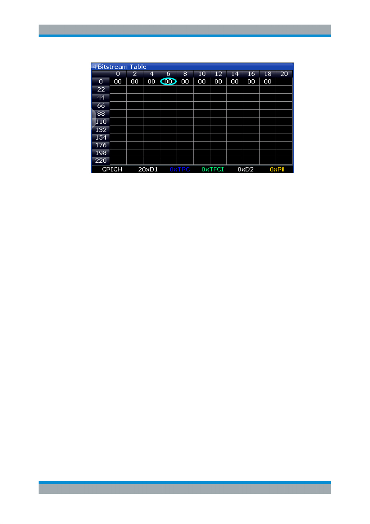
Channel Table
The Channel Table evaluation displays the detected channels and the results of the
code domain power measurement. The channel table can contain a maximum of 512
entries.
In BTS measurements, this corresponds to the 512 codes that can be assigned within
the class of spreading factor 512.
In UE measurements, this corresponds to the 256 codes that can be assigned within
the class of spreading factor 256, with both I and Q branches.
The first entries of the table indicate the channels that must be available in the signal to
be analyzed and any other control channels (see Chapter 4.2, "BTS Channel Types",
on page 43 and Chapter 4.3, "UE Channel Types", on page 47).
The lower part of the table indicates the data channels that are contained in the signal.
If the type of a channel can be fully recognized, based on pilot sequences or modula-
tion type, the type is indicated in the table. In BTS measurements, all other channels
are of type CHAN.
The channels are in descending order according to symbol rates and, within a symbol
rate, in ascending order according to the channel numbers. Therefore, the unassigned
codes are always displayed at the end of the table.
17User Manual 1176.8522.02 ─ 08
R&S®FPS-K72/K73
Figure 3-2: Channel Table display for 3GPP FDD BTS measurements
Remote command:
LAY:ADD? '1',RIGH, CTABle, see LAYout:ADD[:WINDow]? on page 208
TRACe<n>[:DATA]? CTABle
TRACe<n>[:DATA]? PWCDp
TRACe<n>[:DATA]? CWCDp
Table Configuration ← Channel Table
You can configure which parameters are displayed in the Channel Table by doubleclicking the table header.
A "Table Configuration" dialog box is displayed in which you can select the columns to
be displayed.
Measurements and Result Display
Code Domain Analysis
By default, only active channels are displayed. In order to display all channels, including the inactive ones, enable the "Show Inactive Channels" option.
The following parameters of the detected channels are determined by the CDP measurement and can be displayed in the Channel Table evaluation. (For details see
Chapter 3.1.1, "Code Domain Parameters", on page 14.)
18User Manual 1176.8522.02 ─ 08

R&S®FPS-K72/K73
Table 3-4: Code domain power results in the channel table
Measurements and Result Display
Code Domain Analysis
Label Description
Chan Type Type of channel (active channels only)
Ch. SF Number of channel spreading code (0 to [spreading factor-1])
Symbol Rate [ksps] Symbol rate at which the channel is transmitted
In BTS measurements: always
State Active: channel is active and all pilot symbols are correct
Inactive: channel is not active
Pilotf: channel is active, but pilot symbols incomplete or missing
TFCI (BTS measurements only):
Data channel uses TFCI symbols
Mapping (UE measurements only):
Branch the channel is mapped to (I or Q)
PilotL [Bits] Number of pilot bits in the channel
(UE measurements: only for control channel DPCCH)
Pwr Abs [dBm]/Pwr Rel [dBm] Absolute and relative channel power (referred to the CPICH or the
total power of the signal)
T Offs [Chips] (BTS measurements only):
Timing offset
Code Domain Power
Figure 3-3: Code Domain Power Display for 3GPP FDD BTS measurements
The Code Domain Power evaluation shows the power of all possible code channels in
the selected channel slot. The x-axis shows the possible code channels from 0 to the
highest spreading factor. Due to the circumstance that the power is regulated from slot
to slot, the result power may differ between different slots. Detected channels are displayed yellow. The selected code channel is highlighted red. The codes where no
channel could be detected are displayed green.
Note: Effects of missing or incomplete pilot symbols. In "Autosearch" channel detection mode, the application expects specific pilot symbols for DPCH channels. If these
symbols are missing or incomplete, the channel power in the Code Domain Power
evaluation is displayed green at the points of the diagram the channel should appear
due to its spreading code, and a message ("INCORRECT PILOT") is displayed in the
19User Manual 1176.8522.02 ─ 08

R&S®FPS-K72/K73
status bar. In this case, check the pilot symbols for those channels using the Power vs
Slot or the Bitstream evaluations.
Optionally, all QPSK-modulated channels can also be recognized without pilot symbols
(see "HSDPA/UPA" on page 60).
Remote command:
LAY:ADD? '1',RIGH, CDPower, see LAYout:ADD[:WINDow]? on page 208
CALC:MARK:FUNC:WCDP:RES? CDP, see CALCulate<n>:MARKer<m>:FUNCtion:
WCDPower[:BTS]:RESult? on page 221
CALC:MARK:FUNC:WCDP:MS:RES? CDP, see CALCulate<n>:MARKer<m>:
FUNCtion:WCDPower:MS:RESult? on page 223
TRACe<n>[:DATA]? CTABle
TRACe<n>[:DATA]? PWCDp
TRACe<n>[:DATA]? CWCDp
Code Domain Error Power
Code Domain Error Power is the difference in power between the measured and the
ideal signal. The unit is dB. There are no other units for the y-axis.
Measurements and Result Display
Code Domain Analysis
Figure 3-4: Code Domain Error Power Display for 3GPP FDD BTS measurements
Remote command:
LAY:ADD? '1',RIGH, CDEPower, see LAYout:ADD[:WINDow]? on page 208
TRACe<n>[:DATA]? TRACE<1...4>
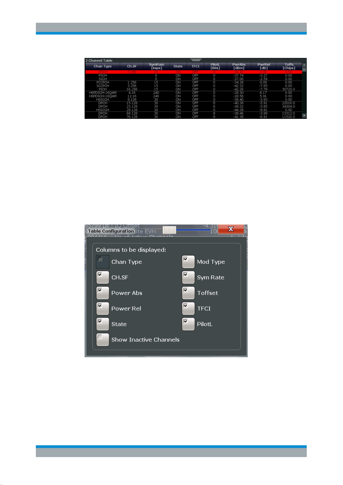
Composite Constellation
The Composite Constellation evaluation analyzes the entire signal for one single slot. If
a large number of channels is to be analyzed, the results are superimposed. In that
case the benefit of this evaluation is limited (senseless).
In Composite Constellation evaluation the constellation points of the 1536 chips are
displayed for the specified slot. This data is determined inside the DSP even before the
channel search. Thus, it is not possible to assign constellation points to channels. The
constellation points are displayed normalized with respect to the total power.
20User Manual 1176.8522.02 ─ 08
R&S®FPS-K72/K73
2560|%100*
²
²
1
0
0
N
x
xs
EVM
N
n
n
N
n
nn
RMS
Figure 3-5: Composite Constellation display for 3GPP FDD BTS measurements
Remote command:
LAY:ADD? '1',RIGH, CCONst, see LAYout:ADD[:WINDow]? on page 208
TRACe<n>[:DATA]? TRACE<1...4>
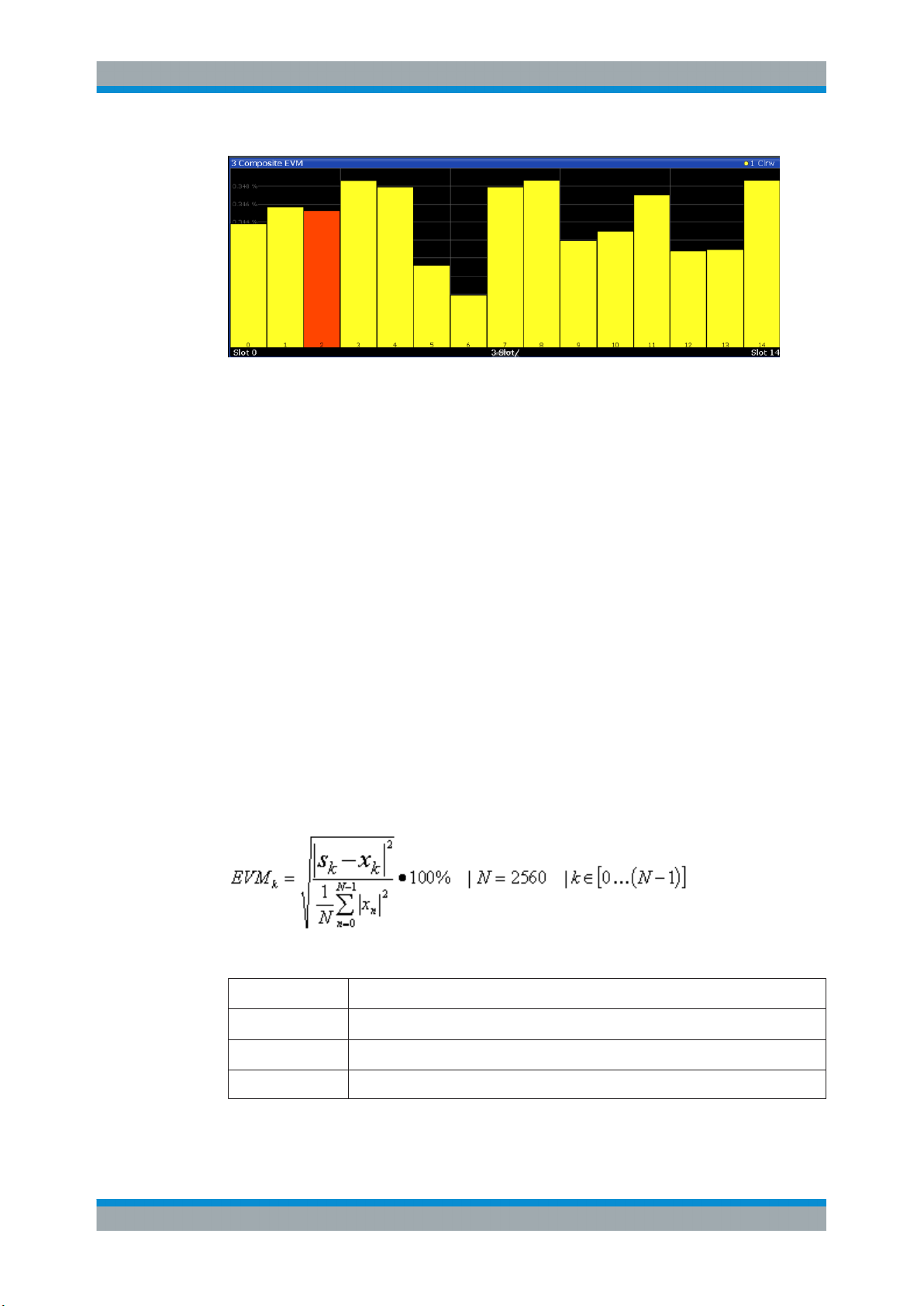
Composite EVM
The Composite EVM evaluation displays the root mean square composite EVM (modulation accuracy) according to the 3GPP specification. The square root is determined of
the mean squared errors between the real and imaginary components of the received
signal and an ideal reference signal (EVM referenced to the total signal). The error is
averaged over all channels for individual slots. The Composite EVM evaluation covers
the entire signal during the entire observation time.
Measurements and Result Display
Code Domain Analysis
where:
EVM
RMS
s
n
x
n
n index number for mean power calculation of received and reference signal.
N number of chips at each CPICH slot
root mean square of the vector error of the composite signal
complex chip value of received signal
complex chip value of reference signal
21User Manual 1176.8522.02 ─ 08
R&S®FPS-K72/K73
Figure 3-6: Composite EVM display for 3GPP FDD BTS measurements
The measurement result consists of one composite EVM measurement value per slot.
In this case, the measurement interval is the slot spacing of the CPICH (timing offset of
0 chips referenced to the beginning of the frame). Only the channels recognized as
active are used to generate the ideal reference signal. If an assigned channel is not
recognized as active since pilot symbols are missing or incomplete, the difference
between the measurement and reference signal and the composite EVM is very high.
Remote command:
LAY:ADD? '1',RIGH, CEVM, see LAYout:ADD[:WINDow]? on page 208
TRACe<n>[:DATA]? TRACE<1...4>
Measurements and Result Display
Code Domain Analysis
EVM vs Chip
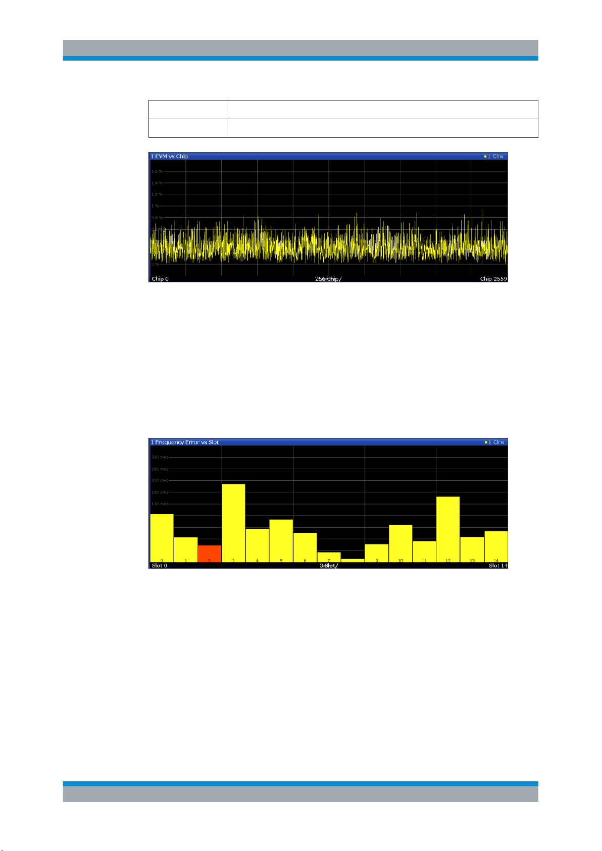
EVM vs Chip activates the Error Vector Magnitude (EVM) versus chip display. The
EVM is displayed for all chips of the selected slot.
Note: In UE measurements, if the measurement interval "Halfslot" is selected for evaluation, 30 slots are displayed instead of the usual 15 (see "Measurement Interval"
on page 109).
The EVM is calculated by the root of the square difference of received signal and reference signal. The reference signal is estimated from the channel configuration of all
active channels. The EVM is related to the square root of the mean power of reference
signal and given in percent.
where:
EVM
s
k
x
k
k
vector error of the chip EVM of chip number k
complex chip value of received signal
complex chip value of reference signal
k index number of the evaluated chip
22User Manual 1176.8522.02 ─ 08
R&S®FPS-K72/K73
Figure 3-7: EVM vs Chip display for 3GPP FDD BTS measurements
Remote command:
LAY:ADD? '1',RIGH, EVMChip, see LAYout:ADD[:WINDow]? on page 208
TRACe<n>[:DATA]? TRACE<1...4>
Measurements and Result Display
Code Domain Analysis
N number of chips at each CPICH slot
n index number for mean power calculation of reference signal
Frequency Error vs Slot
For each value to be displayed, the difference between the frequency error of the corresponding slot to the frequency error of the first (zero) slot is calculated (based on
CPICH slots). This helps eliminate a static frequency offset of the whole signal to achieve a better display of the actual time-dependant frequency diagram.
Figure 3-8: Frequency Error vs Slot display for 3GPP FDD BTS measurements
Note: This display is not available if the Capture Mode is set to "Slot".
Remote command:
LAY:ADD? '1',RIGH, FESLot, see LAYout:ADD[:WINDow]? on page 208
TRACe<n>[:DATA]? ATRACE
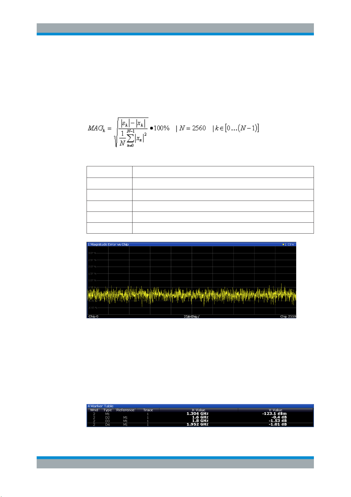
Mag Error vs Chip
The Magnitude Error versus chip display shows the magnitude error for all chips of the
selected slot.
23User Manual 1176.8522.02 ─ 08
R&S®FPS-K72/K73
Note: In UE measurements, if the measurement interval "Halfslot" is selected for eval-
uation, 30 slots are displayed instead of the usual 15 (see "Measurement Interval"
on page 109).
The magnitude error is calculated as the difference of the magnitude of the received
signal to the magnitude of the reference signal. The reference signal is estimated from
the channel configuration of all active channels. The magnitude error is related to the
square root of the mean power of reference signal and given in percent.
Where:
Measurements and Result Display
Code Domain Analysis
MAG
k
s
k
x
k
k Index number of the evaluated chip
N Number of chips at each CPICH slot
n Index number for mean power calculation of reference signal
Figure 3-9: Magnitude Error vs Chip display for 3GPP FDD BTS measurements
Magnitude error of chip number k
Complex chip value of received signal
Complex chip value of reference signal
Remote command:
LAY:ADD? '1',RIGH, MECHip, see LAYout:ADD[:WINDow]? on page 208
TRACe<n>[:DATA]? TRACE<1...4>
Marker Table
Displays a table with the current marker values for the active markers.
This table is displayed automatically if configured accordingly (see " Marker Table Dis-
play " on page 116).
24User Manual 1176.8522.02 ─ 08
R&S®FPS-K72/K73
Remote command:
LAY:ADD? '1',RIGH, MTAB, see LAYout:ADD[:WINDow]? on page 208
Results:
CALCulate<n>:MARKer<m>:X on page 249
CALCulate<n>:MARKer<m>:Y? on page 246
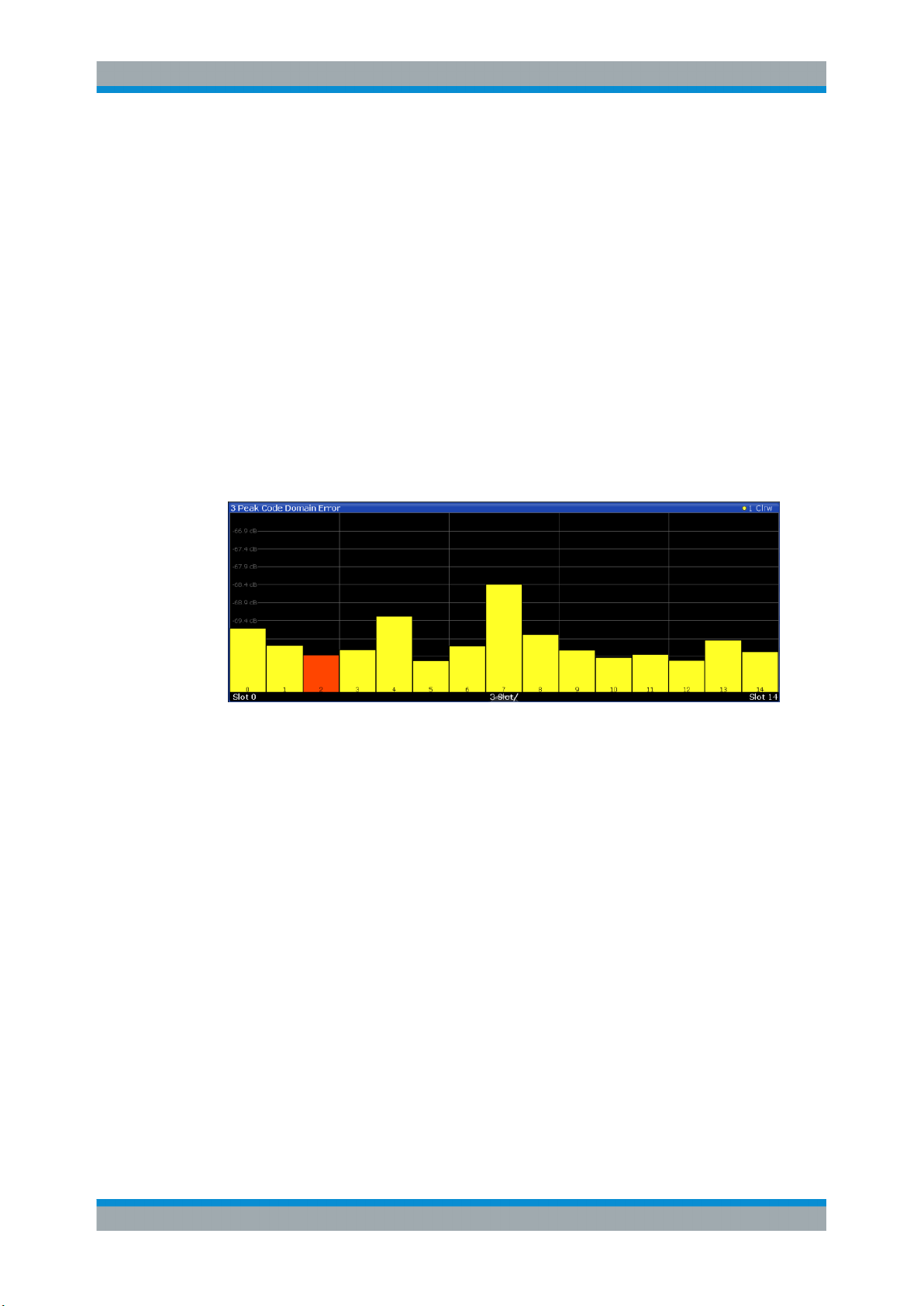
Peak Code Domain Error
In line with the 3GPP specifications, the error between the measurement signal and
the ideal reference signal for a given slot and for all codes is projected onto the various
spreading factors. The result consists of the peak code domain error value per slot.
The measurement interval is the slot spacing of the CPICH (timing offset of 0 chips referenced to the beginning of the frame). Only the channels recognized as active are
used to generate the ideal reference signal for the peak code domain error. If an
assigned channel is not recognized as active since pilot symbols are missing or incomplete, the difference between the measurement and reference signal is very high. This
display is a bar diagram over slots. The unit is dB. The Peak Code Domain Error evaluation covers the entire signal and the entire observation time.
Measurements and Result Display
Code Domain Analysis
Figure 3-10: Peak Code Domain Error display for 3GPP FDD BTS measurements
Remote command:
LAY:ADD? '1',RIGH, PCDerror, see LAYout:ADD[:WINDow]? on page 208
TRACe<n>[:DATA]? TRACE<1...4>
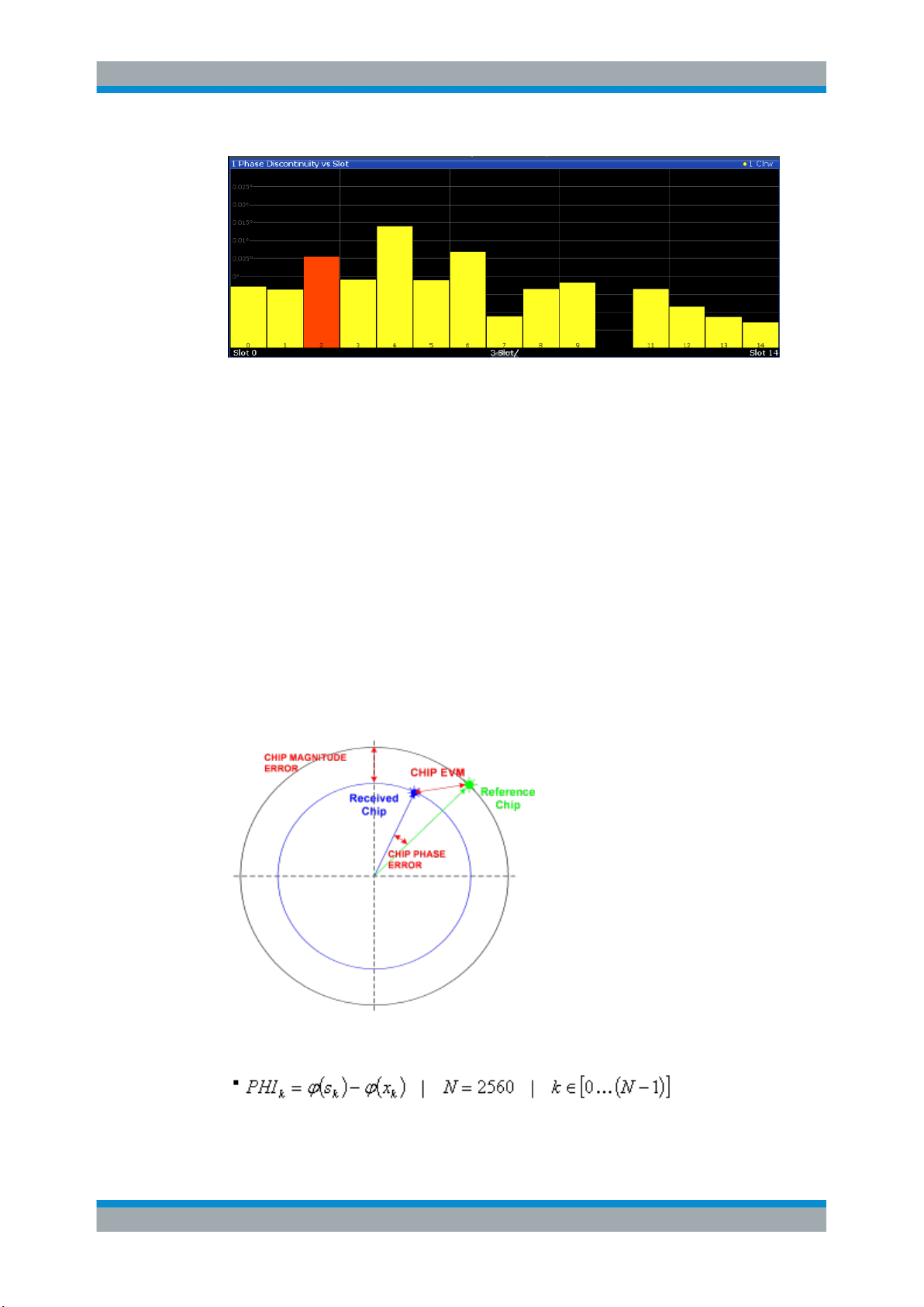
Phase Discontinuity vs Slot
The Phase Discontinuity vs Slot is calculated according to 3GPP specifications. The
phase calculated for each slot is interpolated to both ends of the slot using the frequency shift of that slot. The difference between the phase interpolated for the beginning of one slot and the end of the preceding slot is displayed as the phase discontinuity of that slot.
25User Manual 1176.8522.02 ─ 08
R&S®FPS-K72/K73
Figure 3-11: Phase Discontinuity vs Slot display for 3GPP FDD BTS measurements
Note: This display is not available if the Capture Mode is set to "Slot".
Remote command:
LAY:ADD? '1',RIGH, PDSLot, see LAYout:ADD[:WINDow]? on page 208
TRACe<n>[:DATA]? TRACE<1...4>
Measurements and Result Display
Code Domain Analysis
Phase Error vs Chip
Phase Error vs Chip activates the phase error versus chip display. The phase error is
displayed for all chips of the selected slot.
Note: In UE measurements, if the measurement interval "Halfslot" is selected for evaluation, 30 slots are displayed instead of the usual 15 (see "Measurement Interval"
on page 109).
The phase error is calculated by the difference of the phase of received signal and
phase of reference signal. The reference signal is estimated from the channel configuration of all active channels. The phase error is given in degrees in a range of +180° to
-180°.
Figure 3-12: Calculating the magnitude, phase and vector error per chip
Where:
26User Manual 1176.8522.02 ─ 08
R&S®FPS-K72/K73
Measurements and Result Display
Code Domain Analysis
PHI
k
s
k
x
k
k Index number of the evaluated chip
N Number of chips at each CPICH slot
φ(x) Phase calculation of a complex value
Phase error of chip number k
Complex chip value of received signal
Complex chip value of reference signal
Remote command:
LAY:ADD? '1',RIGH, PECHip, see LAYout:ADD[:WINDow]? on page 208
TRACe<n>[:DATA]? TRACE<1...4>
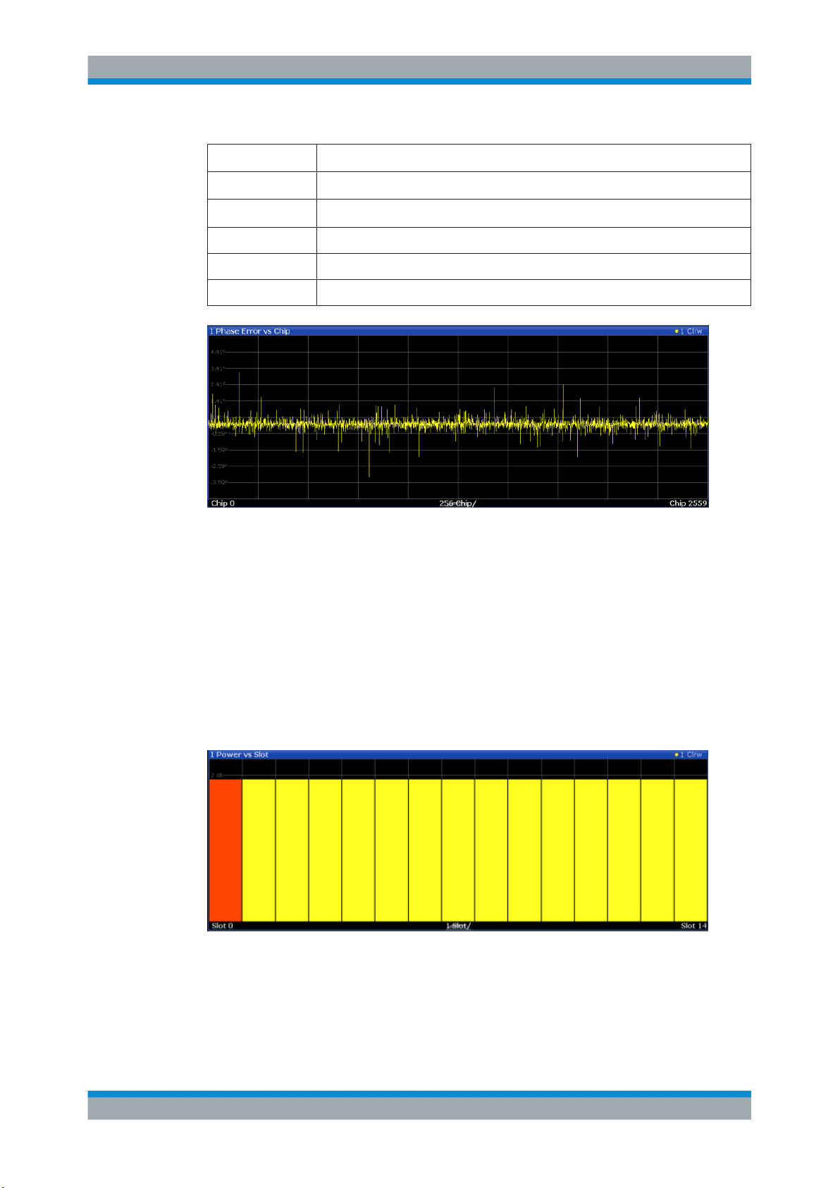
Power vs Slot
The Power vs Slot evaluation displays the power of the selected channel for each slot.
The power is displayed either absolute or relative to the total power of the signal or to
the CPICH channel.
Note: In UE measurements, this evaluation is only available if the analysis mode
"Frame" is selected (see "Capture Mode" on page 79).
If the measurement interval "Halfslot" is selected for evaluation, 30 slots are displayed
instead of the usual 15 (see "Measurement Interval" on page 109).
Figure 3-13: Power vs Slot Display for 3GPP FDD BTS measurements
27User Manual 1176.8522.02 ─ 08

R&S®FPS-K72/K73
If a timing offset of the selected channel in relation to the CPICH channel occurs, the
power is calculated and displayed per channel slot (as opposed to the Code Domain
Power evaluation). However, for reference purposes, the grid in the Power vs Slot diagram indicates the CPICH slots. The first CPICH slot is always slot 0, the grid and
labels of the grid lines do not change. Thus, the channel slots may be shifted in the
diagram grid. The channel slot numbers are indicated within the power bars. The
selected slot is highlighted in the diagram.
Note: This display is not available if the Capture Mode is set to "Slot".
Remote command:
LAY:ADD? '1',RIGH, PSLot, see LAYout:ADD[:WINDow]? on page 208
TRACe<n>[:DATA]? TPVSlot
Power vs Symbol
The Power vs. Symbol evaluation shows the power over the symbol number for the
selected channel and the selected slot. The power is not averaged here. The trace is
drawn using a histogram line algorithm, i.e. only vertical and horizontal lines, no diagonal, linear Interpolation (polygon interpolation). Surfaces are NOT filled.
Measurements and Result Display
Code Domain Analysis
Figure 3-14: Power vs Symbol display for 3GPP FDD BTS measurements
Remote command:
LAY:ADD? '1',RIGH, PSYMbol, see LAYout:ADD[:WINDow]? on page 208
TRACe<n>[:DATA]? TRACE<1...4>
Result Summary
The Result Summary evaluation displays a list of measurement results on the screen.
For details see Chapter 3.1.1, "Code Domain Parameters", on page 14.
Figure 3-15: Result Summary display for 3GPP FDD BTS measurements
28User Manual 1176.8522.02 ─ 08
R&S®FPS-K72/K73
Remote command:
LAY:ADD? '1',RIGH, RSUMmary, see LAYout:ADD[:WINDow]? on page 208
TRACe<n>[:DATA]? TRACE<1...4>
CALCulate<n>:MARKer<m>:FUNCtion:WCDPower[:BTS]:RESult? on page 221
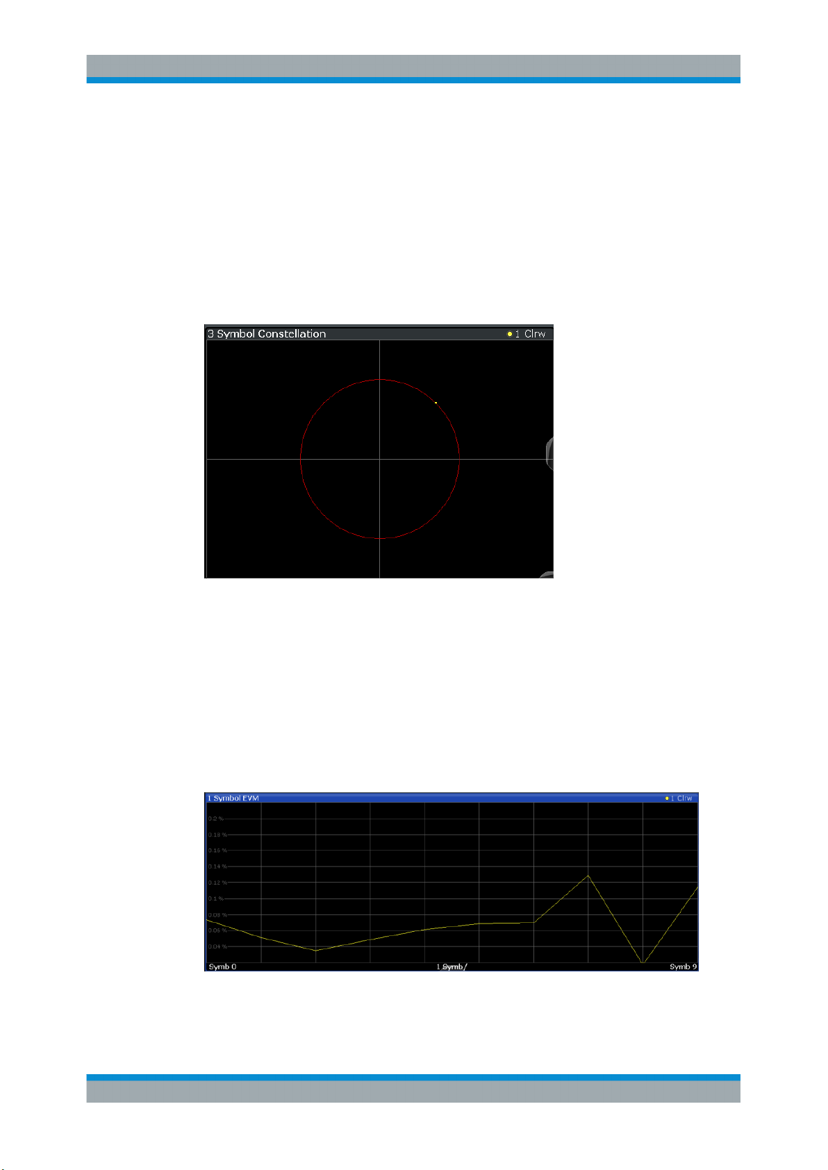
Symbol Constellation
The Symbol Constellation evaluation shows all modulated signals of the selected channel and the selected slot. QPSK constellation points are located on the diagonals (not x
and y-axis) of the constellation diagram. BPSK constellation points are always on the
x-axis.
Measurements and Result Display
Code Domain Analysis
Figure 3-16: Symbol Constellation display for 3GPP FDD BTS measurements
Remote command:
LAY:ADD? '1',RIGH, SCONst, see LAYout:ADD[:WINDow]? on page 208
TRACe<n>[:DATA]? TRACE<1...4>
Symbol EVM
The Symbol EVM evaluation shows the error between the measured signal and the
ideal reference signal in percent for the selected channel and the selected slot. A trace
over all symbols of a slot is drawn. The number of symbols is in the range from 12
(min) to 384 (max). It depends on the symbol rate of the channel.
Figure 3-17: Symbol EVM display for 3GPP FDD BTS measurements
29User Manual 1176.8522.02 ─ 08

R&S®FPS-K72/K73
Remote command:
LAY:ADD? '1',RIGH, SEVM, see LAYout:ADD[:WINDow]? on page 208
TRACe<n>[:DATA]? TRACE<1...4>
Symbol Magnitude Error
The Symbol Magnitude Error is calculated analogous to symbol EVM. The result is one
symbol magnitude error value for each symbol of the slot of a special channel. Positive
values of symbol magnitude error indicate a symbol magnitude that is larger than the
expected ideal value. Negative symbol magnitude errors indicate a symbol magnitude
that is less than the expected ideal value. The symbol magnitude error is the difference
between the magnitude of the received symbol and that of the reference symbol, related to the magnitude of the reference symbol.
Measurements and Result Display
Code Domain Analysis
Figure 3-18: Symbol Magnitude Error display for 3GPP FDD BTS measurements
Remote command:
LAY:ADD? '1',RIGH, SMERror, see LAYout:ADD[:WINDow]? on page 208
TRACe<n>[:DATA]? TRACE<1...4>
Symbol Phase Error
The Symbol Phase Error is calculated analogous to symbol EVM. The result is one
symbol phase error value for each symbol of the slot of a special channel. Positive values of symbol phase error indicate a symbol phase that is larger than the expected
ideal value. Negative symbol phase errors indicate a symbol phase that is less than the
expected ideal value.
Figure 3-19: Symbol Phase Error display for 3GPP FDD BTS measurements
30User Manual 1176.8522.02 ─ 08
 Loading...