


Service Manual Instrument
Universal
Radio Communication Tester
R&SCMU 200
1100.0008.02/53
R&SCMU 300
1100.0008.03
Printed in Germany
1100.4903.82-05
Test and Measurement Division

Trade names are trademarks of the owners
.
R&S®is a registered trademark of Rohde & Schwarz GmbH & Co. KG.

R&S CMU Tabbed Divider Overview
Tabbed Divider Overview
Spare Parts Express Service
List of R&S Representatives
Safety Instructions
Contents
Contents of Manuals for Universal Radio Communication Tester R&S CMU
Tabbed Divider
1 Chapter 1: Performance Test
2 Chapter 2: Adjustment
3 Chapter 3: Repair
4 Chapter 4: Software Update / Installation of Options
5 Chapter 5: Documents
Index
1100.4903.82 RE E-5


Safety Instructions
WARNING
Danger of injuries
When removing the rear feet, the unit can slip out of the cabinet.
Put the unit onto the front handles, before removing the rear feet and taking off the
cabinet. Thus the risk of personal injuries and damages to the unit is avoided.
When mounting the cabinet take care not to pen in the fingers. Also pay attention not
to damage or pull off cables. Screw the rear feet back on immediately after mounting
the cabinet. Do not move the unit with the rear feet missing.
ATTENTION
To avoid damage of electronic components, the operational site must be protected against
electrostatic discharge (ESD).
Wrist strap with cord
Building ground
Floor mat
Heel strap
Ground connection
of operational site
The following two methods of ESD protection may be used together or separately:
• Wrist strap with cord to ground connection
• Conductive floor mat and heel strap combination
1171.0300.62 E-1


CMU Contents
Contents
1 Performance Test
General ..............................................................................................................................................1.1
A) Calibration by an R&S Representative with an ACS Calibration System.........1.1
B) Sending the Instrument to the Factory (Memmingen, Germany)......................1.1
Necessary Documents .............................................................................................................1.1
Measuring Instruments and Auxiliary Equipment.........................................................................1.2
Test Setups ..............................................................................................................................1.3
Reference Frequencies..................................................................................................1.3
TX Level Measurements ................................................................................................1.3
General TX measurements............................................................................................1.4
RX Level measurements................................................................................................1.5
General RX Measurements ...........................................................................................1.5
RX Demodulation Measurements ..................................................................................1.5
Tolerance Analysis ...........................................................................................................................1.6
Manual Test Procedure....................................................................................................................1.7
Selftest .....................................................................................................................................1.7
Interface Test ...........................................................................................................................1.8
IEC-bus Interface ...........................................................................................................1.8
RS–232 Interface ...........................................................................................................1.8
Reference Frequencies ............................................................................................................1.9
REF IN ...........................................................................................................................1.9
REF OUT 1 ..................................................................................................................1.10
REF OUT 2 ..................................................................................................................1.10
TX Frequency Accuracy .........................................................................................................1.11
.......................................................................................................................1.1
TX Frequency Settling Time...................................................................................................1.11
TX Level Error ........................................................................................................................1.11
VSWR ....................................................................................................................................1.11
TX Level Settling Time ...........................................................................................................1.12
TX Harmonics ........................................................................................................................1.12
TX Non Harmonics .................................................................................................................1.12
TX In-Band Spurious Signals .................................................................................................1.12
TX Fixed Spurious Signals .....................................................................................................1.13
TX SSB Phase Noise .............................................................................................................1.13
TX Residual FM......................................................................................................................1.13
TX Residual AM .....................................................................................................................1.13
1100.4903.82 3 E-5

Contents CMU
TX Carrier/Sideband Suppression, Max. Distortion ...............................................................1.14
RX Power Meter (Frequency-Selective).................................................................................1.14
RX Power Meter (Wideband) .................................................................................................1.14
RX Harmonics ........................................................................................................................1.15
RX Spurious Response / Image Rejection .............................................................................1.15
RX SSB Phase Noise.............................................................................................................1.15
RX Residual FM/AM...............................................................................................................1.16
RX Dynamic/ Average Noise Level ........................................................................................1.16
Options for R&S CMU200 ......................................................................................................1.17
GSM-MS ......................................................................................................................1.17
TX GSM Modulation.....................................................................................................1.17
RX GSM Dem odulation........................................................................................1.17
CDMA2000.............................................................................................................................1.18
TX CDMA2000 Modulation ..........................................................................................1.18
RX CDMA2000 Dem odulation.................................................................................1.19
WCDMA .......................................................................................................................1.20
TX WCDMA Modulation...............................................................................................1.20
RX WCDMA Dem odulation .....................................................................................1.20
Function Test with Mobile Stations (R&S CMU200)...............................................................1.21
GSM mobile test ..........................................................................................................1.21
CDMA mobile test ........................................................................................................1.21
CDMA2000 mobile test ................................................................................................1.21
IS136-mobile test .........................................................................................................1.21
AMPS-mobile test ........................................................................................................1.22
Test Report......................................................................................................................................1.23
2 Adjustment....................................................................................................................................2.1
Manual Adjustment ..........................................................................................................................2.1
Measuring Instruments and Auxiliary Equipment .....................................................................2.1
Preparing the Instrument..........................................................................................................2.2
Adjusting the + 5 VDC Reference Voltage ...............................................................................2.2
Adjusting the 10 MHz Reference Frequency............................................................................2.3
TCXO .............................................................................................................................2.3
OCXO REFERENCE OSC. R&S CMU -B11 .................................................................2.3
OCXO REFERENCE OSC. R&S CMU -B12 .................................................................2.3
Automatic Adjustment of Module Data ..........................................................................................2.4
Preparing the adjustment .........................................................................................................2.4
Performing the adjustment .......................................................................................................2.4
1100.4903.82 4 E-5

CMU Contents
3 Repair ..............................................................................................................................................3.1
Instrument Design and Function Description ...............................................................................3.1
Block diagram ..........................................................................................................................3.2
Instrument Frame .....................................................................................................................3.3
ear of Instrument Frame ........................................................................................................3.3
R
Front of Instrument Frame .......................................................................................................3.3
Cooling the Instrument .............................................................................................................3.4
FRONT MODULE ....................................................................................................................3.5
POWER SUPPLY ....................................................................................................................3.6
MOTHERBOARD .....................................................................................................................3.7
REFERENCE BOARD .............................................................................................................3.9
Option OCXO REFERENCE OSC. R&S CMU-B11 or B12 ...................................................3.10
RF FRONTEND .....................................................................................................................3.10
RXTX BOARD1 ......................................................................................................................3.11
DIGITAL BOARD....................................................................................................................3.13
Option UNIVERSAL SIGNALLING UNIT R&S CMU-B21 Var02 ...........................................3.14
Option UNIVERSAL SIGNALING UNIT R&S CMU-B21 Var 14/54 .......................................3.16
Option AUDIO-GEN. + ANA. R&S CMU-B41.........................................................................3.18
Option WCDMA L1COPRO R&S CMU-B66/68/76/78 ..........................................................3.19
Option CDMA (IS95) Signaling Unit R&S CMU-B81 ..............................................................3.21
Option CDMA2000 Signaling Unit R&S-B83 Var12 ...............................................................3.22
Option CDMA2000 Signaling Unit R&S CMU-B83 Var22 ......................................................3.23
MODULE Replacement...................................................................................................................3.25
Replacing the FRONT MODULE ...........................................................................................3.25
Opening the instrument and removing the FRONT MODULE ........................3.25
Installing the new FRONT MODULE and completing the instrument .............3.26
Putting into operation ......................................................................................3.26
Replacing the FRONT MODULE CONTROLLER in the FRONT MODULE ..........................3.27
Opening the instrument and removing the FRONT MODULE ........................3.27
Removing the FRONT MODULE CONTROLLER ..........................................3.28
Installing the new FRONT MODULE CONTROLLER .....................................3.28
Installing the option again and completing the instruments ............................3.28
Putting into operation ......................................................................................3.29
Replacing the Lithium Battery in the FRONT MODULE.........................................................3.30
Opening the instrument and removing the FRONT MODULE ........................3.30
Removing the lithium battery and installing the new battery ...........................3.31
Completing the instrument ..............................................................................3.32
Putting into operation ......................................................................................3.32
Replacing the Hard Disk in the FRONT MODULE .................................................................3.33
Opening the instrument and removing the FRONT MODULE ........................3.33
Removing the hard disk from the FRONT MODULE ......................................3.33
Installing the new hard disk.............................................................................3.33
Putting into operation ......................................................................................3.33
1100.4903.82 5 E-5

Contents CMU
Replacing the Memory Modules in the FRONT MODULE .....................................................3.34
Opening the instrument and removing the FRONT MODULE ........................3.34
Making the memory modules accessible ........................................................3.35
Removing the memory module .......................................................................3.35
Installing the new memory module and completing the instrument ................3.35
Putting into operation ......................................................................................3.36
Replacing the LCD and/or DC/AC Converter in the FRONT MODULE .................................3.37
Opening the instrument and removing the FRONT MODULE ........................3.37
Making the LCD accessible.............................................................................3.38
Removing the LCD and/or DC/AC Converter..................................................3.38
Installing the new LCD and/or DC/AC converter and compl. the instrument ..3.38
Putting into operation ......................................................................................3.38
Replacing the Keyboard Membrane and/or Mat on the FRONT MODULE............................3.39
Opening the instrument and removing the FRONT MODULE ........................3.39
Removing the membrane................................................................................3.40
Installing the new membrane and completing the instrument.........................3.40
Putting into operation ......................................................................................3.40
Replacing the Labeling Panel on the FRONT MODULE........................................................3.41
Removing the old labeling panel .....................................................................3.41
Installing the new labeling panel and completing the instrument ....................3.41
Putting into operation ......................................................................................3.41
Replacing the Options FLOPPY DISK DRIVE R&S CMU-B61 or PCMCIA INTERFACE......3.42
Opening the instrument and removing the FRONT MODULE ........................3.42
Replacing the option........................................................................................3.43
Completing the instrument and putting into operation.....................................3.43
Replacing the RF FRONTEND ..............................................................................................3.44
Opening the instrument and removing the RF FRONTEND ...........................3.44
Installing the new RF FRONTEND MODULE and compl. the instrument.......3.44
Automatic module data adjustment.................................................................3.44
Replacing the REFERENCE BOARD ....................................................................................3.45
Opening the instrument and removing the REFERENCE BOARD .................3.45
Installing the new REFERENCE BOARD and completing the instrument ......3.45
Automatic module data adjustment.................................................................3.45
Replacing the RXTX BOARD1 ...............................................................................................3.46
Opening the instrument and removing the RXTX BOARD1 ...........................3.46
Installing the new RXTX BOARD1 and completing the instrument.................3.46
Automatic module data adjustment.................................................................3.46
Replacing the TR-CORRECTION MODULE in the RXTX BOARD1 .....................................3.47
Opening the instrument and removing the TR-CORRECTION MODULE ......3.47
Installing the new TR-CORRECTION BOARD and compl. the instrument.....3.47
Automatic module data adjustment.................................................................3.47
Replacing the DIGITAL BOARD.............................................................................................3.48
Opening the instrument and removing the DIGITAL BOARD .........................3.48
Installing the new DIGITAL BOARD and completing the instrument ..............3.48
Automatic module data adjustment.................................................................3.48
Replacing the MODULES: ADC MODULE1, DDC MODULE1, TXDSP MODULE1, AUC
MODULE1 in the DIGITAL BOARD .......................................................................................3.49
Opening the instrument and removing the modules .......................................3.49
Installing the new sandwich module and completing the instrument ..............3.49
Automatic module data adjustment.................................................................3.50
1100.4903.82 6 E-5

CMU Contents
Replacing the Option OCXO REFERENCE OSC. R&S CMU-B11 or R&S CMU-B12 ..........3.51
Opening the instrument and rem. the OPTION OCXO REFERENCE OSC...3.51
Installing the new OPTION OCXO REFERENCE OSC. and
completing the instrument ...............................................................................3.51
Manual OCXO adjustment ..............................................................................3.51
Replacing the Option UNIVERSAL SIGNALLING UNIT R&S CMU-B21 Var02 ...................3.52
Opening the instrument and removing the OPTION UNIV. SIGN. UNIT ........3.52
Installing the new OPTION UNIV. SIGN. UNIT and compl. the instrument ....3.52
Automatic module data adjustment.................................................................3.52
Replacing the MODULES: DSP MODULE0/1, IQOUT MODULE, BLUETOOTH MODULE,
SPEECH CODEC R&S CMU-B52 (INCLUDES DSP MODULE3) in the UNIV. SIGN. UNIT
Var02......................................................................................................................................3.53
Opening the instrument and removing the modules .......................................3.53
Installing the new sandwich module and completing the instrument ..............3.53
Automatic module data adjustment.................................................................3.54
Replacing the Option UNIVERSAL SIGNALLING UNIT CMU-B21 Var14/54........................3.55
Opening the instrument and removing the OPTION UNIV. SIGN. UNIT ........3.55
Installing the new OPTION UNIV. SIGN. UNIT and compl. the instrument ....3.55
Automatic module data adjustment.................................................................3.55
Replacing the MODULES: SPEECH CODEC, BLUETOOTH MODULE, MC 68K, DSP
MODULE, POWER PC MODULE, OPTION SPEECH CODEC CMU-B52VAR 14
in the UNIV. SIGN. UNIT Var14/54 ........................................................................................3.56
Opening the instrument and removing the modules .......................................3.56
Installing the new sandwich module and completing the instrument ..............3.56
Automatic module data adjustment.................................................................3.57
Replacing the Option WCDMA L1COPRO CMU-B66/68/76/78.............................................3.57
Opening the instrument and removing the OPTION WCDMA L1COPRO......3.57
Installing the new OPTION UNIV. SIGN. UNIT and compl. the instrument ....3.57
Automatic module data adjustment.................................................................3.57
Replacing the MODULES: WCDMATX MODULE, TX-FEC MODULE, WDDC MODULE,
RX-FEC MODULE , in the WCDMA L1COPRO CMU-B66/68/76/78 ....................................3.58
Opening the instrument and removing the modules .......................................3.58
Installing the new sandwich module and completing the instrument ..............3.59
Automatic module data adjustment.................................................................3.59
Replacing the Option CDMA2000 Signaling Unit CMU-B83 Var12........................................3.59
Opening the instrument and removing the OPTION
CDMA2000 SIGNALING UNIT........................................................................3.59
Installing the new OPTION CDMA2000 SIGNALING UNIT and
completing the instrument ...............................................................................3.60
Automatic module data adjustment.................................................................3.60
Replacing the MODULES: ACCESS MODULE CMU-B82, SPEECH CODEC MODULE
CMU-B85, HDR MODULE CMU-B88 in the CDMA2000 Signaling Unit CMU-B83 Var12.....3.60
Opening the instrument and removing the modules .......................................3.60
Installing the new sandwich module and completing the instrument ..............3.60
Automatic module data adjustment.................................................................3.61
Replacing the Option CDMA2000 Signaling Unit CMU-B83 Var22........................................3.61
Opening the instrument and removing the OPTION
CDMA2000 SIGNALING UNIT........................................................................3.61
Installing the new OPTION CDMA2000 SIGNALING UNIT and
completing the instrument ...............................................................................3.62
Automatic module data adjustment.................................................................3.62
1100.4903.82 7 E-5

Contents CMU
Replacing the MODULES: 1xEV-DO MODULE CMU-B89, SPEECH CODEC MODULE
CMU-B85 VAR22, POWER QUICC3 MODULE in the CDMA2000 Signaling Unit
MU-B83 Var22 .....................................................................................................................3.62
C
Opening the instrument and removing the modules .......................................3.62
Installing the new sandwich module and completing the instrument ..............3.63
Automatic module data adjustment.................................................................3.63
Replacing the Option AUDIO-GEN. + ANA. CMU-B41 ..........................................................3.64
Opening the instrument and removing the Option AUDIO-GEN. + ANA. .......3.64
Installing the new Option AUDIO-GEN. + ANA. and compl. the instrument ...3.64
Automatic module data adjustment.................................................................3.64
Replacing the POWER SUPPLY ...........................................................................................3.65
Removing the POWER SUPPLY ....................................................................3.65
Installing the new POWER SUPPLY...............................................................3.65
Replacing the Instrument Fan ................................................................................................3.66
Opening the instrument and removing the fan ................................................3.66
Installing the new fan and completing the instrument .....................................3.66
Replacing the MOTHERBOARD (1100.0908.02) ..................................................................3.67
MOTHERBOARD1 (big MOTHERBOARD) .................................................................3.67
Opening the instrument and removing MOTHERBOARD1 ............................3.67
Installing the new MOTHERBOARD1 and completing the instrument............3.67
MOTHERBOARD2 (small MOTHERBOARD) .............................................................3.68
Opening the instrument and removing MOTHERBOARD2 ............................3.68
Installing the new MOTHERBOARD2 and completing the instrument............3.68
FRONTPANEL BOARD (at the front of the instrument frame) ....................................3.68
Opening the instrument and removing the FRONTPANEL BOARD...............3.68
Installing the new FRONTPANEL BOARD and completing the instrument ....3.68
REARPANEL BOARD1 (Interface board for Standard Connectors at the Rear
of the Instrument Frame) .............................................................................................3.69
Opening the instrument and removing the REARPANEL BOARD1 ...............3.69
Installing the new REARPANEL BOARD1 and completing the instrument.....3.69
REARPANEL BOARD2 (Interface Board for Further Connectors at the Rear of the
Instrument Frame) .......................................................................................................3.69
Opening the Instrument and removing the REARPANEL BOARD2 ...............3.69
Installing the new REARPANEL BOARD2 and completing the instrument.....3.69
Replacing the MOTHERBOARD (1100.2352.02)...........................................................................3.70
MOTHERBOARD1 (big MOTHERBOARD) .................................................................3.70
Opening the instrument and removing MOTHERBOARD1 ............................3.70
Installing the new MOTHERBOARD1 and completing the instrument............3.70
MOTHERBOARD2 (small MOTHERBOARD) .............................................................3.71
Opening the instrument and removing MOTHERBOARD2 ............................3.71
Installing the new MOTHERBOARD2 and completing the instrument............3.71
FRONTPANEL BOARD (at the front of the instrument frame) ....................................3.71
Opening the instrument and removing the FRONTPANEL BOARD...............3.71
Installing the new FRONTPANEL BOARD and completing the instrument ....3.71
REARPANEL BOARD2 (Interface Board for Further Connectors at the Rear
of the Instrument Frame) Opening the Instrument and removing
the REARPANEL BOARD2..........................................................................................3.72
Installing the new REARPANEL BOARD2 and completing the instrument.....3.72
1100.4903.82 8 E-5

CMU Tables
Troubleshooting .............................................................................................................................3.73
Troubleshooting using the LEDs (H1 to H8) on the MOTHERBOARD ..................................3.74
Troubleshooting using the SELFTEST Menu for Modules .....................................................3.76
More troubleshooting..............................................................................................................3.79
General errors on the transmitter side of the R&S CMU........................................................3.79
General errors on the receiver side of the R&S CMU ............................................................3.80
4 Software Update/Installing Options ...................................................................................4.1
New Installation of the CMU Software............................................................................................4.1
Software Update via PCMCIA INTERFACE.............................................................................4.1
Software Update via FLOPPY DISK DRIVE ............................................................................4.1
Performing a Software Update .................................................................................................4.2
Reinstalling the Old Software .........................................................................................................4.3
Loading Software as long as there is no VersionManager in the R&S CMU ..............................4.3
Installing the Options.......................................................................................................................4.4
SW Packages for various network tests R&S CMU-Kxx ......................................................4.4
5 Documents ....................................................................................................................................5.1
Module and Cable Exchange...........................................................................................................5.1
1100.4903.82 9 E-5

Tables CMU
Tables
Table 1-1 Measuring instruments and auxiliary equipment for manual performance test......................1.2
Table 1-2 Test report ............................................................................................................................1.18
Table 2-1 Measuring instruments and auxiliary equipment for manual adjustment of the R&S CMU ...2.1
Table 5-1 List of power cables available ................................................................................................5.2
1100.4903.82 10 E-5

R&S CMU Index
Index
DSP Module0/1.................. 3.53, 3.55, 3.58, 3.60, 3.62
A
ADC Module1 (DIGITAL Board) ................................... 3.13
Adjustment
+ 5 VDC Reference Voltage..................................... 2.2
10 MHz Reference-Frequency .................................2.3
Automatic of Module Data........................................ 2.4
AUC Module1 (DIGITAL Board) ................................... 3.14
AUDIO-GEN. + ANA., R&S CMU-B41.......................... 3.18
Auxiliary means.............................................................. 1.2
B
Block diagram ................................................................ 3.2
C
CDMA (IS95) Signalling Unit ...................... 3.21, 3.22, 3.23
Circuit documents (basic unit) ........................................ 5.3
Cooling the instrument ...................................................3.4
D
DDC Module1 (DIGITAL Board)................................... 3.13
DIGITAL Board............................................................. 3.13
Documents..................................................................... 5.1
Drawing of all CMU spare parts.......................... See annex
DSP Module (UNIV. SIGN. Unit) ......................... 3.15, 3.16
F
Fan See cooling the instrument
FLOPPY DISK DRIVE (Software Update) ...................... 4.1
FRONT Module.............................................................. 3.5
FRONTPANEL Board.............................................. 3.7, 3.8
Function test with Mobile Stations................................ 1.21
FLOPPY Disk Drive R&S CMU-B61 .......................3.42
Front Module..........................................................3.25
FRONT Module Controller......................................3.27
FRONTPANEL Board....................................3.68, 3.71
Hard Disk ...............................................................3.33
Instrument fan ........................................................3.66
IQOUT Module................... 3.53, 3.55, 3.58, 3.60, 3.62
Keyboard Membrane ..............................................3.39
Labeling Panel........................................................3.41
LCD........................................................................3.37
Lithium Battery .......................................................3.30
Mat .........................................................................3.39
Memory Modules....................................................3.34
Motherboard .................................................. 3.67, 3.70
Motherboard1 ................................................ 3.67, 3.70
Motherboard2 ................................................ 3.68, 3.71
Option AUDIO-GEN. + ANA. CMU-B41..................3.63
Option OCXO REFERENCE OSC..........................3.51
Option SPEECH CODEC ... 3.53, 3.55, 3.58, 3.60, 3.62
PCMCIA Interface R&S CMU-B62..........................3.42
POWER SUPPLY...................................................3.65
REARPANEL Board1 .............................................3.69
REARPANEL Board2 ....................................3.69, 3.72
REFERENCE Board...............................................3.45
RF Frontend...........................................................3.44
RXTX Board1.........................................................3.46
TR-CORRECTION Module.....................................3.47
TXDSP Module1.....................................................3.49
UNIVERSAL SIGNALLING Uni
t.......................................... 3.52, 3.55, 3.57, 3.59, 3.61
Motherboard ...................................................................3.7
Motherboard1 ..........................................................3.7, 3.8
Motherboard2 ..........................................................3.7, 3.8
N
Netclock generation........................................................3.9
H
Hard disk (FRONT Module)............................................ 3.5
I
Instrument design........................................................... 3.1
Instrument frame ............................................................ 3.3
Interface test
IEC bus.................................................................... 1.8
RS-232.....................................................................1.8
IQOUT Module (UNIV. SIGN. Unit) ..................... 3.15, 3.19
L
LCD (FRONT Module).................................................... 3.5
Loudspeaker .................................................................. 3.3
M
Manual Test Procedure .................................................. 1.7
Maximum distortion ...................................................... 1.14
Measuring instruments ................................................... 1.2
Module replacement
ADC Module1......................................................... 3.49
AUC Module1......................................................... 3.49
DDC Module1 ........................................................ 3.49
DIGITAL Board ...................................................... 3.48
O
OCXO
Adjustment ...............................................................2.3
REFERENCE OSC. R&S CMU-B11 or B12 (Option)
...............................................................................3.10
Options
Installing...................................................................4.4
List ...........................................................................4.4
Overtemperature protection (POWER SUPPLY) ............3.6
P
PCMCIA INTERFACE (Software Update).......................4.1
Performance Test ...........................................................1.1
Power cables..................................................................5.2
Power Factor Correction (PFC, POWER SUPPLY) ........3.6
POWER SUPPLY...........................................................3.6
POWERGOOD signal (POWER SUPPLY) .....................3.6
R
R&S CMU-B21 ...........................................3.14, 3.16, 3.19
R&S CMU-B41 .............................................................3.18
R&S CMU-B81 ...........................................3.21, 3.22, 3.23
R&S CMU-K21 (Option)..................................................4.4
REARPANEL Board1 .....................................................3.7
1100.4903.82 I.1 E-5

R&S CMU Index
REARPANEL Board2 ..................................................... 3.8
REFERENCE Board....................................................... 3.9
Reference frequencies ...................................................1.9
Repair ............................................................................3.1
RF Frontend................................................................. 3.10
RX Dynamic / average noise level................................ 1.16
RX GSM Demodulation .............................. 1.17, 1.19, 1.20
RX Harmonics .............................................................. 1.15
RX Power meter (Frequency selective) ........................1.14
RX Power meter (Wideband)........................................ 1.14
RX Residual FM/AM.....................................................1.16
RX Spurious response / image rejection....................... 1.15
RX SSB Phase Noise...................................................1.15
RXTX Board1............................................................... 3.11
S
Selftest........................................................................... 1.7
Software Update
New installation........................................................4.1
Performing ............................................................... 4.2
Reinstalling the Old Software................................... 4.3
Spare parts (order)......................................................... 5.1
SPEECH CODEC (UNIV. SIGN. UNIT)3.15, 3.17, 3.19,
3.22, 3.24
Spinwheel (FRONT Module) .......................................... 3.5
STANDBY circuit (POWER SUPPLY) ............................ 3.6
STANDBY/ON signal (POWER SUPPLY)...................... 3.6
T
TCXO
Adjustment ...............................................................2.3
Function ...................................................................3.9
Test report....................................................................1.23
Tolerance analysis..........................................................1.6
Troubleshooting
General errors ........................................................3.79
using the error messages .......................................3.78
using the LEDs.......................................................3.74
using the SELFTEST Menu for Modules ................ 3.76
TX carrier/sideband suppression ..................................1.14
TX Frequency Accuracy ...............................................1.11
TX Frequency settling time ...........................................1.11
TX GSM Modulation ................................... 1.17, 1.18, 1.20
TX Harmonics...............................................................1.12
TX Level Error ..............................................................1.11
TX Level Settling time...................................................1.12
TX Nonharmonics .........................................................1.12
TX Residual AM............................................................1.13
TX Residual FM............................................................1.13
TX SSB Phase Noise ...................................................1.13
TXDSP Module1 (DIGITAL Board) ...............................3.14
U
Universal Signalling Unit............................. 3.14, 3.16, 3.19
Update (software) ...........................................................4.2
V
VersionManager (loading)...............................................4.3
VSWR ..........................................................................1.11
1100.4903.82 I.2 E-5

R&S CMU Documentation
Contents of Manuals for Universal Radio Communication Tester R&S CMU200/ R&S CMU300
Service Manual Instrument
This service manual for Universal Radio Communication Tester R&S CMU provides information on
checking the instrument for compliance with rated specifications, as well as on adjustment, repair
and troubleshooting. It further contains all the information necessary for repairing the instrument by
the replacement of modules.
The service manual comprises five chapters and an annex (chapter 5) containing the R&S CMU circuit
documentation:
Chapter 1 Provides all the information necessary to check R&S CMU for compliance with
rated specifications. The required test equipment is included, too.
Chapter 2 Describes the adjustment of the +5 VDC reference source and of the 10-MHz
reference frequency source as well as the software-controlled adjustment of individual module data following module replacement.
Chapter 3 Describes the design of R&S CMU as well as simple measures for repair and
fault
diagnosis, in particular the replacement of modules and access to hardware settings by means of service commands.
Chapter 4 Contains information on the extension and modification of R&S CMU by installing
instrument software and retrofitting options.
Chapter 5 Contains spare parts lists and exploded views of R&S CMU.
Operating Manual
In the operating manual for R&S CMU basic unit you will find information about the technical specifications of R&S CMU, the controls and connectors on the front and rear panel, necessary steps for
putting the instrument into operation, the basic operating concept, manual and remote control.
For introduction typical measurement tasks are explained in detail using the functions of the user interface and program examples.
The operating manual contains all information on the characteristics, operation and remote control of
the R&S CMU including RF and Audio measurements. It further provides hints on preventive maintenance and fault diagnosis by means of warnings and error messages output by the unit.
Service Manual Modules
The service manual modules is not delivered with the instrument but may be obtained from your R&S
service department using the order number 1100.4903.92.
Service manual modules contains information about the individual modules of R&S CMU. This comprises the test and adjustment of the modules, fault detection within the modules and the interface
description.
1100.4903.82 0.1 E-5


R&S CMU General
1 Performance Test
his chapter provides the necessary information for checking the technical data of the R&S CMU.
T
Please read the general notes on the test procedure on page 1.7 first. Then follows a list of the
measuring equipment required for the performance test; a form for the test report is to be found at the
end of this chapter.
The adjustment of the instrument for restoring the data integrity and the measuring equipment required
for this purpose will be described in chapter 2 of this service manual.
General
The technical data of a R&S CMU can be checked in the following ways:
A) Calibration by an R&S Representative with an ACS Calibration System
Advantages
• Automatic procedure
• Small measurement uncertainties
• Calibration and readjustment
• In most cases, the instrument does not have to leave the country
B) Sending the Instrument to the Factory (Memmingen, Germany)
Advantages
• Automatic procedure at the final test setup
• Minimum measurement uncertainties
• Calibration and readjustment
Necessary Documents
• Operating manual R&S CMU200/R&S CMU300
• Data sheet R&S CMU200
Note: It is recommended to read the following journal on the subjects "measurement uncertainty"
and "tolerance analysis": ETSI Technical Report ETR 028, June 1997
1100.4903.82 1.1 E-5

Measuring Instruments and Auxiliary Equipment R&S CMU
Measuring Instruments and Auxiliary Equipment
Table 1-1 Measuring instruments and auxiliary equipment for manual performance test
Item Type of instrument Required characteristics Appropriate device R & S
1 Signal generator 100 kHz to 2.7 GHz,
2 Spectrum analyzer 100 kHz to 7 GHz,
3 Power meter R&S NRVD with sensors
4 Power amplifier 100 kHz to 2.7 GHz,
5 Harmonics filter attenuate the harmonics of the
6 Directional coupler 50 MHz to 2.7 GHz,
7 Network analyzer
or VSWR Bridge
Generation of a
GSM/CDMA2000/WCDMA
signal (dummy burst)
Demodulation of
GSM/CDMA2000/WCDMA
signals
Pout = 100 W
power amplifiers to min 30 dBc
up to 100 W
100 kHz to 2.7 GHz R&S ZVR
R&S SME03
R&S SMIQ03 with
options B42/B60
R&S FSE with
R&S FSE-B7
R&S FSIQ-7 with options
B4/B5/B7/B11/B12/B70/
K71
R&S FSP–3
R&S NRV-Z4
R&S NRV-Z51
RX measurements
RX measurements
RX measurements
R&S ZRC
order number
1038.6002.03
1125.5555.03
1066.3010.20/30
1119.5005.17
1164.4391.03
RX measurements,
1043.0009.61 Reflection coefficient/
Use
RX measurements
TX measurements
TX measurements
VSWR
RF connectors
1100.4903.82 1.2 E-5
R&S CMU Measuring Instruments and Auxiliary Equipment
REF1
REF2
TX1
Test Setups
The quality of the test setup has an effect on the measurement procedures.
Note: Make sure to use only high-quality coax cables and coax connectors as well as calibrated
measuring equipment.
Reference Frequencies
Test setup REF1:
Spectrum
Analyzer
(FSE
or
FSIQ)
GEN
REFIN
DUT
(CMU)
R
F3 OUT
10 MHz Reference Freq.
Test setup REF2:
Spectrum
Analyzer
(FSE or
FSIQ)
DUT
(CMU)
REF IN
REF OUT 2
10 MHz Reference Freq.
TX Level Measurements
Test setup TX1, TX2, TX3, TX4 (depending on level range):
Normalize spectrum analyzer (FSIQ) to wideband power meter (NRVD) at Max. Level setting of the
R&S CMU (test setups TX1, TX2, TX3).
The attenuator of the spectrum analyzer must be held at this position over 60 dB.
Normalize spectrum analyzer with preamplifier to spectrum analyzer at last level (test setups TX3,
TX4).
The attenuator of the spectrum analyzer must be held at this position over 60 dB.
DUT
(CMU)
+5 dBm
RF3OUT
NRV-Z51
NRVD
1100.4903.82 1.3 E-5
Measuring Instruments and Auxiliary Equipment R&S CMU
TX2
TX3
TX4
ext. Trigger input
TX5
-33 dBm/
DUT
(CMU)
DUT
(CMU)
-16 dBm
R
F1 /
R
F2
-93 dBm to -33 dBm/
-76 dBm to -16 dBm/
-55 dBm to +5 dBm
RF1 /
RF2 /
R
F3 OUT
10 MHz Reference Freq.
NRV-Z4
FSIQ or FSE
NRVD
-130 dBm to -93 dBm/
-117 dBm to -76 dBm/
DUT
(CMU)
-90 dBm to -55 dBm
RF1/
RF2/
RF3 OUT
10 MHz Reference Freq.
General TX measurements
Test setup TX5:
AUX3, pin2
DUT
(CMU)
RF1, RF2, RF3 OUT
10 MHz Reference Freq.
RF-PreAmp
36 dB
FSE
or FSIQ
Spectrum
analyzer
(FSE or
FSIQ)
1100.4903.82 1.4 E-5
R&S CMU Measuring Instruments and Auxiliary Equipment
RX3
RX4
RX Level measurements
Test setup RX1, RX2 (depending on level range):
RX1
NRVZ4
NRVD
GEN
Power
Ampl.
depending on max.
level of power splitter
RX2
GEN
Power
Ampl.
General RX Measurements
Test setup RX3:
LPF
LPF
Power
Splitter
direct. coupl
-30 dB
NRV-
Z4
DUT
(CMU)
NRVD
DUT
(CMU)
GEN
RF, RF2, RF4IN
10 MHz Reference Freq.
DUT
(CMU)
RX Demodulation Measurements
Test setup RX4:
Demodulator
GEN
RF4IN
10 MHz Reference Freq.
DUT
(CMU)
IF3RX CH1
10 MHz Reference Freq.
1100.4903.82 1.5 E-5
(FSE with
FSE-B7 or
FSIQ)

Tolerance Analysis R&S CMU
Tolerance Analysis
Due to the small measurement uncertainty of the R&S CMU, the measuring equipment must meet
stringent requirements. Since the measurement uncertainty of the measuring equipment to be achieved
depends on the test setup used, it is recommended to perform a tolerance analysis.
To be able to trace back errors in the measurement, the measurement uncertainty should also be
indicated in the test report.
The tolerances given in the test report refer to the values specified in the data sheet, ie the
measurement uncertainties of the test setup used are to be taken into account as well.
Unless otherwise specified, the specified tolerances are always to be observed.
Note: Please take into account the ETSI Technical Report ETR 028.
The given tolerances refer to R&S CMU data sheet 04/99.
1100.4903.82 1.6 E-5

R&S CMU Manual Test Procedure
Manual Test Procedure
Some additional measurements can only be performed using a mobile phone via the normal operating
menus of the R&S CMU. These measurements are described in the section 'Function Test with Mobile
Stations'.
The suggested frequencies and levels at which the measurements should be performed have been
selected according to the instrument concept. The user can of course also select other frequencies and
levels within the scope of values guaranteed in the data sheet.
Note: Before testing the rated specifications, allow the instrument to warm up for at least 15 min.
The ambient temperature should be 23 °C to 26 °C.
Selftest
The R&S CMU offers various selftest options for checking the functioning and for troubleshooting.
Before carrying out the performance test, the Maintanance menu in the BASE function group should be
called up and the following selftests should be performed:
• Continuous Selftest
• 1
Preparation:
Test: Select the individual test in the BASE (MAINTENANCE) menu and check the results
Note: The Continuous Selftest combines the System Selftest and Internal RF Loop Selftest. In
1
To obtain more detailed information start the following tests:
4/32 RF Loop Test
Start user SW of the R&S CMU (switch on instrument).
(Continuous Selftest, 1
this test, only a passed/failed message with error output is indicated. In case of errors, an
error file ‘cst.err’ is created in addition.
4/32 RF Loop Test: Selftest RF Path RF1RF4 IN and RF3 OUTRF2 via external
N-coax cable by power measurements via internal generator and analyzer. In this test, all
measured values are indicated.
System selftest:
Internal RF Loop Selftest:
FE Selftest:
REF Selftest:
4/32 RF Loop Test).
Selftest of the instrument for diagnostic voltages; only a
passed/failed message with error output is indicated.
Selftest of the RF path by means of power measurements
via internal generator and analyzer. All measured values
are indicated.
Selftest of the RF FRONTEND module via diagnostic
voltages. All measured values are indicated.
Selftest of the REFERENCE BOARD module via diagnostic
voltages. All measured values are indicated.
DIG Selftest:
RXTX1 Selftest:
To obtain more detailed information start the following tests(depending on options and
R&S CMU SW versions):
1100.4903.82 1.7 E-5
Selftest of the DIGITAL BOARD module via diagnostic
voltages. All measured values are indicated
Selftest of the RXTX1 BOARD module via diagnostic
voltages. All measured values are indicated.

Manual Test Procedure R&S CMU
QIF Selftest:
I
AUXTX Selftest:
Linkhandler Selftest:
IF3 Selftest:
B83 Selftest:
RXTX2 Selftest:
Selftest of the R&S CMU-B17 IQIF BOARD module via
iagnostic voltages. All measured values are indicated.
d
Selftest of the R&S CMU-B95 AUXTX or R&S CMU-B96
AUXTX W BOARD module via diagnostic voltages. All
measured values are indicated.
Selftest of the R&S CMU-B21 Var02 ULH and/or R&S
CMU-B21 Var14 USU and/or R&S CMU-B66/B68/B76/B78
L1COPRO BOARD module. All measured values are
indicated.
IF3 Level Selftest of the RXTX BOARD module (greater
than Board version 11) via diagnostic voltages. All
measured values are indicated.
Selftest of the R&S CMU-B83 CDMA LH BOARD module.
All measured values are indicated.
Selftest of the RXTX2 BOARD (if available) module via
diagnostic voltages. All measured values are indicated.
Interface Test
IEC-bus Interface
Preparation:
Test: Send the string ‘*IDN?<CR><NL>’ from the controller to the R&S CMU and
Connect the IEC-bus interfaces of the R&S CMU and the controller via IEC-
bus cables.
read the reply STRING of the R&S CMU.
The reply STRING must contain the following message:
‘ROHDE & SCHWARZ,R&S CMU<Var>,<Ser_Nr>,<Firmware_Vers._Nr>’
RS–232 Interface
Preparation:
Test: Send the string ‘*IDN?<CR><NL>’ from the controller to the R&S CMU and
Connect the RS–232 interfaces of the R&S CMU and the controller via null-
modem cables
Set the RS–232 interface of the controller to 8 data bits, 1 start bit, 1 stop bit, no
parity bit, XON/XOFF handshake and 19200 baud.
read the reply string of the R&S CMU.
The reply string must contain the following message:
‘ROHDE & SCHWARZ,R&S CMU<Var>,<Ser_Nr>,<Firmware_Vers._No>’
1100.4903.82 1.8 E-5

R&S CMU Manual Test Procedure
Reference Frequencies
For different range of adjustment of the internal reference oscillator, the synchronization with an external
reference frequency is checked.
Note: The resolution of the frequency counter/analyzer should be max. 1/10 of the maximum
permissible deviation.
REF IN
The frequency and level ranges and the pull-in range are checked. The signal generator and the
frequency counter must be synchronized (test setup REF1).
Preparation:
Control: Set R&S CMU to external reference 52 MHz, RF 1 GHz (menu RF ANALYZER/
Test: Use frequency counter to measure frequency deviation from 1 GHz.
Feed in at REF IN: 52 MHz sinewave, 0.5 V(rms)
Connect frequency counter to RF3 OUT.
GENERATOR.)
Preparation:
Control: Set R&S CMU to external reference 1 MHz, RF 1 GHz.
Test: Use frequency counter to measure frequency deviation from 1 GHz.
Preparation:
Control: Set R&S CMU to external reference 10 MHz, RF 1 GHz.
Test: Use frequency counter to measure frequency deviation from 1.000 005 000 GHz.
Preparation:
Control: Set R&S CMU to external reference 10 MHz, RF 1 GHz.
Test: Use frequency counter to measure frequency deviation from 0.999 995 GHz.
Feed in at REF IN: 1 MHz sinewave, 0.5 V(rms).
Connect frequency counter to RF3 OUT.
Feed in at REF IN: 10.000 050 MHz sinewave, 1.4 V(rms).
Connect frequency counter to RF3 OUT.
Feed in at REF IN: 9.999 950 MHz sinewave, 1.4 V(rms).
Connect frequency counter to RF3 OUT.
1100.4903.82 1.9 E-5

Manual Test Procedure R&S CMU
REF OUT 1
The level and frequency are checked.
nt. 10 MHz:
I
REF IN
signal:
Set R&S CMU to internal reference.
Measure at REF OUT 1: 10 MHz, level > 1.4 V(pp).
Set R&S CMU to external reference.
Feed in at REF IN: 52 MHz TTL, (as an alternative +16 dBm from signal)
Measure at REF OUT 1: 52 MHz, level > 1.4 V(pp).
Measure at REF OUT 1: frequency 52 MHz ± 1 Hz
Feed in at REF IN: 1 MHz TTL, (as an alternative +16 dBm from signal
generator).
Measure at REF OUT 1: 1 MHz, level > 0.5 V(rms) (1.4 V(pp)).
Measure at REF OUT 1: frequency 1 MHz ± 1 Hz.
REF OUT 2
The level and frequency are checked. The R&S CMU and the frequency counter must be synchronized
(test setup REF2).
REF OUT 2
signal
13 MHz or 10 MHz:
Set R&S CMU to external reference.
Feed in at REF IN: 10 MHz sinewave, 0.5 V(rms).
Set R&S CMU to REF OUT 2 13 MHz or 10 MHz (depending on SW; menu
Connection Control – Sync.).
Measure at REF OUT 2: 13 MHz or 10 MHz, level > 1.0 V(pp).
Measure at REF OUT 2: frequency 13 MHz or 10 MHz ± 1 Hz.
1100.4903.82 1.10 E-5

R&S CMU Manual Test Procedure
TX Frequency Accuracy
Preparation: Test setup TX5, but R&S CMU not synchronized with frequency counter/analyzer
and no external trigger.
R&S CMU connector RF3 OUT.
Control: Set R&S CMU to desired frequency, level 0 dBm.
Test: Determine frequency deviation from nominal frequency.
TX Frequency Settling Time
Preparation: Test setup TX5, in addition trigger cable from R&S CMU (D-sub connector AUX3,
pin2) to analyzer.
R&S CMU connector RF3 OUT.
R&S CMU: Ramping off, hopping on, F1 = start freq., F2 = stop freq.
Analyzer: Sweep time 1 ms, Center = stop frequency, FM demodulation,
real time off, BW 50 kHz, 1 kHz/Div, external trigger, Slope
negative
Control: Set R&S CMU to desired frequencies and hopping, level 0 dBm.
Test: Time from trigger point when the specified offset (< 1 kHz) from the stop
frequency is reached.
TX Level Error
Preparation: Test setup TX1 to TX4 (depending on level range).
Control: Set R&S CMU to desired connector, frequency and level (RF Analyzer must
be OFF).
Test: Measure the TX level of the R&S CMU.
Note: The given frequencies and levels are suggested values. Of course, it is also possible to use
other values for the measurement.
VSWR
Preparation:
Control:
Test: Measure VSWR at 10 MHz, 900 MHz, 1800 MHz, 2700 MHz.
Connect (scalar) network analyzer to RF1, RF2, RF3 OUT, RF4 IN one after
the other.
Cable losses must be corrected.
R&S CMU: Switch generator on and set level to minimum (–130 dBm or
–90 dBm), switch RF wideband analyzer on (RF1/RF2/RF4 IN).
1100.4903.82 1.11 E-5

Manual Test Procedure R&S CMU
point to the point in time when the nominal
TX Level Settling Time
Preparation:
Control: Set R&S CMU to frequency = 1 GHz, specified level and ramping mode.
Test: The time period from the trigger
Test setup TX5, in addition trigger cable from R&S CMU (D-sub connector AUX3,
pin2) to analyzer.
R&S CMU: Connector RF3 OUT 1GHz, Ramping On, Hopping Off.
Analyzer: Sweep time = 40 µs, Center = 1 GHz , Span = 0, RBW = 10
MHz, external trigger.
level < 0.5 dB has been reached is measured.
TX Harmonics
Preparation: Test setup TX5, no external trigger
Analyzer: Center = 2 x f
Control: Set R&S CMU to connector RF1, specified frequency, level = –27 dBm.
Test: The suppression of the signal at twice or three times the nominal frequency is
measured relative to the nominal signal.
Control: Set R&S CMU to connector RF2, specified frequency, level = –10 dBm.
Test: The suppression of the signal at twice or three times the nominal frequency is
measured relative to the nominal signal.
Control: Set R&S CMU to connector RF3 OUT, specified frequency, level = +10 dBm.
Test: The suppression of the signal at twice and three times the nominal frequency is
measured relative to the nominal signal.
or Center = 3 x f
nom
, Span = 1 MHz.
nom
TX Non Harmonics
TX In-Band Spurious Signals
Spurious signals within the specified frequency bands are checked.
Preparation Test setup TX5, no external trigger
Analyzer Start/Stop = specified frequency range, RBW = 100 kHz
Control: Set R&S CMU to connector RF3 OUT, specified setting frequency, level = 0
dBm.
Test: The suppression of the signal is measured at the test frequency relative to the set
signal.
1100.4903.82 1.12 E-5

R&S CMU Manual Test Procedure
TX Fixed Spurious Signals
Fixed spurious signals are checked.
Preparation: Test setup TX5, no external trigger.
Analyzer: Center = specified test frequency, RBW = 100 kHz, Span = 1 MHz.
Control: Set R&S CMU to connector RF3 OUT, specified setting frequency, specified
level.
Test: The suppression of the signal is measured at the test frequency relative to the set
signal.
TX SSB Phase Noise
Preparation Test setup TX5, no external trigger
Control: Set R&S CMU generator to specified RF frequency.
Test Measure the phase noise at the specified spacing from the carrier.
Connect spectrum analyzer or modulation analyzer to RF3 OUT.
Output level at RF3 OUT 0 dBm,
Analyzer to specified center frequency,
Span = 50 kHz to 5 MHz, RBW = Span/500,
Noise measurement function.
TX Residual FM
Preparation: Test setup TX5, no external trigger.
Control: Set R&S CMU generator to the specified RF frequency.
Test: The residual FM with the specified weighting is measured.
Connect spectrum analyzer or modulation analyzer to RF1.
Output level at RF1 –27 dBm, analyzer to specified center frequency, FM
demodulator.
TX Residual AM
Preparation: Test setup TX5, no external trigger.
Control: Set R&S CMU generator to specified RF frequency.
Test: The residual AM with the specified weighting is measured.
1100.4903.82 1.13 E-5
Connect spectrum analyzer or modulation analyzer to RF1.
Output level at RF1 –27 dBm, analyzer to specified center frequency, AM
demodulator.

Manual Test Procedure R&S CMU
TX Carrier/Sideband Suppression, Max. Distortion
The modulation quality of the analog IQ modulator of the R&S CMU is measured.
Preparation Test setup TX5, no external trigger.
Connect spectrum analyzer to RF3 OUT.
Control: Set R&S CMU generator to specified RF frequency.
Output level at RF3 OUT, 0 dBm,
Switch on RF generator with offset modulation, 300- kHz baseband filter,
Set analyzer to center frequency f
= 1000 MHz, Span = 300 kHz / 3 MHz
c
Test: The suppression of the carrier at f
+ f
signal at f
.
od
c
m
is measured relative to the useful sideband
c
RX Power Meter (Frequency-Selective)
Preparation: Test setup RX1, RX2 (depending on level range).
Control: Set R&S CMU to desired RX frequency and level and Input in menu RF
ANALYZER/ GENERATOR.
Measuring Bandwidth = 1 kHz.
Test: Measure RX level measurement accuracy of R&S CMU.
Note: The given frequencies and levels are suggested values; of course, it is also possible to use
other values for the measurement.
RX Power Meter (Wideband)
Preparation Test setup RX1, RX2 (depending on level range).
Control: Set R&S CMU to desired RX connector, frequency and level and Input in
menu RF Analyzer/ Generator.
Measuring Bandwidth = Wide
Test: Measure RX level measurement accuracy of R&S CMU.
Note: The given frequencies and levels are suggested values; of course, it is also possible to use
other values for the measurement.
1100.4903.82 1.14 E-5

R&S CMU Manual Test Procedure
RX Harmonics
Preparation: Test setup RX3,
Generator = f
; level = 0 dBm.
in
Control: Set R&S CMU to connector RF2, Max Level = 2 dBm.
Test: The suppression of the signal at twice and three times the input frequency is
measured relative to the input signal.
Preparation:
Test setup RX3
Generator = f
n
i
; level = –2 dBm
Control: Set R&S CMU to connector RF4 IN, Max Level = 0 dBm.
Test: The suppression of the signal at twice and three times of input frequency is
measured relative to the input signal.
RX Spurious Response / Image Rejection
Preparation: Test setup RX3,
Control: Set R&S CMU to connector RF2, Max Level = 2 dBm, Mode = Low Distortion
Generator = f
; level = 0 dBm.
in
Test: The suppression of the spurious or image signal is measured relative to the
input signal.
Preparation:
Test setup RX3,
Generator = f
; level = –2 dBm.
in
Control: Set R&S CMU to connector RF4 IN, Max level = 0 dBm, Mode = Low
Distortion
Test: The suppression of the spurious or image signal is measured relative to the input
signal.
RX SSB Phase Noise
Preparation: Test setup RX3,
Control: Set R&S CMU to connector RF2, Max Level = 10 dBm and to desired
Test: The measurement is taken with a small test bandwidth at different carrier offsets.
Generator = f
+ df ; level = 10 dBm.
iCMU
frequency.
Switch on frequency-selective power meter.
Note: The input level is +10 dBm, RBW = 100 Hz
Phase noise = measured value –10 dB –21 dB.
1100.4903.82 1.15 E-5

Manual Test Procedure R&S CMU
RX Residual FM/AM
Preparation: Test setup RX4,
Control: Set R&S CMU to connector RF4 IN, Max Level = –20 dBm and to desired
Test: The measurement is taken with an external FM/AM demodulation instrument (FSE
Generator = f
frequency.
Switch on frequency-selective power meter.
with FSE-B7) via the IF3RXCH1 BNC connector at the rear panel of the R&S CMU.
Set the FSE to desired frequency, ref. level, AF filters.
; level = –20 dBm.
iCMU
RX Dynamic/ Average Noise Level
Preparation: No signal is fed in, R&S CMU generator is OFF.
Control: Set R&S CMU to given receive frequency, Max. Level, Bandwidth, Mode = Low
Noise.
Test: Use frequency-selective power meter, measurement bandwidth = 1 kHz / 500 kHz,
measured value in dB below reference level (Max. Level).
1100.4903.82 1.16 E-5

R&S CMU Manual Test Procedure
Options for R&S CMU200
GSM-MS
The following tests can be carried out only if the GSM-MS (R&S CMU-K2x) software options are
installed and enabled by entering a key code.
TX GSM Modulation
Only with options R&S CMU-K21, R&S CMU-K22, R&S CMU-K23 or R&S CMU-K24:
The GSM phase/frequency error of a TX path is measured.
Preparation: Test setup TX5:
Control: Set R&S CMU generator to specified RF frequency.
Test: Phase (rms and peak) and frequency errors are measured according to GSM
Connect spectrum analyzer FSIQ to RF3 OUT.
Output level at RF3 OUT 10 dBm
Training Sequence -> GSM0;
Bit Mod. -> PRBS
Transmission -> BURST
Settings at spectrum analyzer FSIQ:
Mode -> Digital Standards -> GSM
Mode -> Meas Result -> Result_Length -> 146 (the useful part normally comprises
147 bits, however, the FSIQ can be set to an integer number of bits only and
therefore cuts off 0.5 bits at the beginning and at the end of the measurement
range)
Trigger -> Find Sync -> ON
Trigger -> Sync Pattern -> gsm_bts0 (training sequence GSM0)
Trigger -> Sync Offset -> 60 symbols
recommendation.
RX GSM Dem odulation
Only with option R&S CMU-K21, R&S CMU-K22, R&S CMU-K23 or R&S CMU-K24:
The GSM phase/frequency error of a RX path is measured.
Preparation: Connect GSM signal generator to RF2 (test setup RX3).
Control: Signal generator SMIQ: GSM signal at given frequency, level according to table,
Test:
1100.4903.82 1.17 E-5
The signal generator must be synchronized with the R&S CMU via the 10 MHz
reference frequency.
bursted with the following settings:
Digital Std -> GSM/EDGE -> State -> ON;
Digital Std -> GSM/EDGE -> Select Slot -> Burst type -> NORM
Digital Std -> GSM/EDGE -> Select Slot -> Slot Level -> FULL
Digital Std -> GSM/EDGE -> Select Slot -> Data -> PN9
Digital Std -> GSM/EDGE -> Select Slot -> TSC -> TSC0
R&S CMU: GSM Non Signalling, training sequence = GSM 0, trigger source = IF
Power, Trigger Level = Medium
Measure GSM phase error (rms and peak) as well as frequency error.

Manual Test Procedure R&S CMU
CDMA2000
The following tests can be carried out only if the CDMA2000 (R&S CMU-K8x) software options are
installed and enabled by entering a key code.
TX CDMA2000 Modulation
Only with options R&S CMU-K83, R&S CMU-K84, R&S CMU-K85 or R&S CMU-K86:
The CDMA2000 modulation parameter of a TX path is measured.
Preparation: Test setup TX5:
Control: Set R&S CMU generator to specified RF frequency.
Connect spectrum analyzer FSIQ to RF3 OUT.
Settings at R&S CMU:
CDMA2000 450 MHz (CDMA2000 Cellular, CDMA2000 PCS, CDMA2000 IMT-
2000) Signaling Connection Control
CDMA Power = -7 dBm
Traffic level = OFF, Paging level = OFF, Sync. level = OFF, Pilot level = - 7 dB,
OCNS level = OFF
RF3OUT
RF Channel = 1, 2016 CDMA2000 450 MHz
= 1, 777 CDMA2000 Cellular
= 1, 1199 CDMA2000 PCS
= 0, 1199 CDMA2000 IMT-2000
Switch on Generator
Remote (in CDMA2000 NSig):
OUTP:STAT RF3
SOURce:RFGenerator:LEVel:OCNS:ENABle OFF
SOURce:RFGenerator:FREQuency 870.03MHZ
SOURce:RFGenerator:POWer:CDMA -7
SOURce:RFGenerator:LEVel:FPICh -7
SOURce:RFGenerator:LEVel:FSYNc OFF
SOURce:RFGenerator:LEVel:FPCH OFF
SOURce:RFGenerator:LEVel:FFCH OFF
INIT:RFGenerator
Settings at FSIQ 7:
Set Frequency 460.000 MHz, 493.48 MHz CDMA2000 450 MHz
870.03 MHz, 893.31 MHz CDMA2000 Cellular
1930.05 MHz, 1989.95 MHz CDMA2000 PCS
2110.000 MHz, 2169.95 MHz CDMA2000 IMT-2000
Set Reference Level
Rho Factor Measurement , Carrier Suppression
Annotation:
FSIQ can perform this measurement only on one active channel
The R&S CMU CDMA2000 Output level will only be equal to displayed CDMA
power with OCNS=AUTO.
Test: Rho factor and carrier suppression are measured according to CDMA2000
recommendation.
1100.4903.82 1.18 E-5

R&S CMU Manual Test Procedure
RX CDMA2000 Dem odulation
Only with option R&S CMU-K83, R&S CMU-K84, R&S CMU-K85 or R&S CMU-K86:
The CDMA2000 modulation parameter of a RX path is measured.
Preparation: Connect CDMA2000 signal generator to RF2 (test setup RX3).
Control: Signal Generator SMIQ:
CDMA RX Measurement for RC1,2(O-QPSK)
The signal generator must be synchronized with the R&S CMU via the 10 MHz
reference frequency.
Reset
Set Frequency 450.000 MHz, 483.480 MHz CDMA2000 450 MHz
825.03 MHz, 848.31 MHz CDMA2000 Cellular
1850.05 MHz, 1909.95 MHz CDMA2000 PCS
1920.000 MHz, 1979.950 MHz CDMA2000 IMT-2000
Set Level -10 dBm
Select DIGITAL STD IS95
STATE ON
MODE REV_LINK
TRIGGER MODE AUTO
R&S CMU:
CDMA 800 (CDMA 1900) NSig Analyzer/Generator
RF Channel = 1, 2016 CDMA2000 450 MHz
= 1, 777 CDMA2000 Cellular
= 1, 1199 CDMA2000 PCS
= 0, 1199 CDMA2000 IMT-2000
Analyzer Mode MAN
Expected power -10 dBm (Max Level = input level +6dB, to prevent overload in
R&S CMU SW)
RF2
Trigger: FREERUN
Remote:
INP:STAT RF2;
TRIGger[:SEQuence]:SOURce[:OQPSk]FRUN
SENSE:LEVEL:MODE MAN
LEV:MAX -10
[SENSe]:RFANalyzer:FREQuency [MHz]
READ[:SCALar]:MODulation:MQUality:OQPSk?
READ[:SCALar]:MODulation:MQUality:OQPSk?
<MSPower> {Value} dBm
<Waveform Quality> {Value}
<CarrierFrequencyError> {Value} Hz
<TransmitTimeError> {Value} s
<CarrierFeedtrough> {Value} dB
RESERVED NAN
<SidebandSuppresLower> {Value} dB
<SidebandSuppresUpper> {Value} dB
<Bursts Out Of Tolerance> {Value} %
Test:
Measure waveform quality as well as frequency measurement error.
1100.4903.82 1.19 E-5

Manual Test Procedure R&S CMU
WCDMA
he following tests can be carried out only if the WCDMA (R&S CMU-K66) software options are
T
installed and enabled by entering a key code.
TX WCDMA Modulation
Only with option R&S CMU-K66:
The WCDMA modulation parameter of a TX path is measured.
Preparation: Test setup TX5:
Control: Set R&S CMU generator to specified RF frequency.
Connect spectrum analyzer FSIQ to RF2 and RF3 OUT.
Settings at R&S CMU:
R&S CMU-WCDMA-generator:
Total level = CPICH-level
relative level : SCHs = –35dB, P-CCPCH = –35 dB, DPDCH = 0dB,
DPCCH/DPDCH = 0dB, PICH level = –35dB
DPCH Codechannel = 4 (R&S CMU SW Base >= V3.07 necessary)
Generator-Mode: 3GPP Reference Measurement Channel 12.2kbit/s and 384
kbit/s (entspricht Symbolrate 480ksps)
Settings at FSIQ 7:
WCDMA BTS Analyser, Code Domain Power,
Display-Result: Result summary
Select Channel Number:
16 für 12.2 kbit/s, 256 für 384 kbit/s
Test: Global EVM are measured.
Code Channel Conf: 480ksps für 384 kbit/s
RX WCDMA Dem odulation
Only with option R&S CMU-K65:
The WCDMA demodulation quality of a RX path is measured.
Preparation: Connect WCDMA signal generator to RF2 and RF4 IN (test setup RX3).
Control: Set R&S CMU analyzer and SMIQ to specified RF frequency.
WCDMA RX Measurement
The signal generator must be synchronized with the R&S CMU via the 10 MHz
reference frequency.
Signal Generator SMIQ:
Signal Typ 2
Low_EVM-Mode
R&S CMU:
Application WCDMA
RF mode = Manual
RF Attenuation = Low Noise
Statistical Count = 10
Test:
1100.4903.82 1.20 E-5
Measure EVM rms, I/Q origin offset, I/Q imbalance, carrier frequency error as
well as peak code domain error.

R&S CMU Manual Test Procedure
Function Test with Mobile Stations (R&S CMU200)
GSM mobile test
Only with Option R&S CMU-K21, R&S CMU-K22, R&S CMU- K23 or R&S CMU-K24.
Location Update
Call to MS
Call Release
Call from MS
Echo test
Power ramp, Phase/Frequency error measurement
Handover GSM900/1800
CDMA mobile test
Only with Option R&S CMU-K81, R&S CMU-K82.
Location Update
Call to MS
Call Release
Call from MS
Echo test
CDMA2000 mobile test
Only with Option R&S CMU-K83, R&S CMU-K84,R&S CMU-K85, R&S CMU-K86.
Location Update
Call to MS
Call Release
Call from MS
Echo test
IS136-mobile test
Only with Option R&S CMU-K27, R&S CMU-K28.
Location Update
Call to MS
Call Release
Call from MS
Echo test
1100.4903.82 1.21 E-5

Manual Test Procedure R&S CMU
AMPS-mobile test
Only with Option R&S CMU-K29.
Location Update
Call to MS
Call Release
Call from MS
Echo test
1100.4903.82 1.22 E-5

R&S CMU Test Report
Test Report
ROHDE & SCHWARZ Universal Radiocommunication Tester R&S CMU 1100.0008
Serial number:
Test person:
Date:
Signature:
Table 1-2 Test report
Item
No.
Ambient temperature during calibration 23 26 °C
Description
Measure-
ment
to section
Min. Actual Max.
Measurement
General Tests
CONTINUOUS SELFTEST Passed passed
1 4/3 2 RF LOOP TEST Passed passed
Adjusting +5 V DC REFERENCE
VOLTAGE
Adjusting TCXO 10 MHz at
RF3 OUT 1 GHz
(if none of the options R&S CMU-B11
or R&S CMU-B12 is installed)
Adjusting R&S CMU-B11 OCXO 10
MHz at RF3 OUT 1GHz
(if option R&S CMU-B11is installed)
Adjusting R&S CMU-B12 OCXO 10
MHz at RF3 OUT 1GHz
(if option R&S CMU-B12 is installed)
Chapter 2 4.999 5.001 mV
Chapter 2 –50 +50 Hz
Chapter 2 –10 +5 Hz
Chapter 2 –10 +5 Hz
uncertainty
Unit
REF IN 52 MHz REF IN –1 +1 Hz
REF IN 1 MHz –1 +1 Hz
REF IN 10 MHz +50 Hz –1 +1 Hz
REF IN 10 MHz –50 Hz –1 +1 Hz
REF OUT 1 Int 10 MHz REF OUT 1 1.4 5 V(pp)
REF OUT 1 52 MHz 1.4 5 V(pp)
REF OUT 1 52 MHz –1 +1 Hz
REF OUT 1 1 MHz 1.4 5 V(pp)
REF OUT 1 1 MHz –1 +1 Hz
1100.4903.82 1.23 E-5

Test Report R&S CMU
Item
No.
REF OUT 2 13 MHz or 10 MHz REF OUT 2 1 5 V(pp)
REF OUT 2 13 MHz or 10 MHz –1 +1 Hz
Description
Measure-
ment
to section
Min. Actual Max.
Measurement
uncertainty
TX Frequency Accuracy
TX Frequency accuracy 2200 MHz TX
Frequency
accuracy
–2200
–220
–11
+2200
(TCXO),
+220
(B11),
+11
(B12)
Hz
TX Frequency Settling
TX frequency settling time
F1 = 100 MHz ->F2 = 200 MHz to
<1 kHz
TX frequency settling time
F1 = 1800 MHz ->F2 = 1900 MHz to
<1 kHz
TX frequency settling time
F1 = 2200 MHz ->F2 = 2100 MHz to
<1 kHz
TX frequency settling time
F1 = 100 MHz ->F2 = 2200 MHz to
<1 kHz
TX frequency settling time
F1 = 2000 MHz ->F2 = 100 MHz to
<1 kHz
TX
Frequency
settling
400
400
400
400
400
Unit
µs
µs
µs
µs
µs
VSWR
VSWR RF1 10 MHz VSWR 1.2
VSWR RF1 900 MHz 1.2
VSWR RF1 1800 MHz 1.2
VSWR RF1 2700 MHz 1.6
VSWR RF2 10 MHz 1.2
VSWR RF2 900 MHz 1.2
VSWR RF2 1800 MHz 1.2
VSWR RF2 2700 MHz 1.6
VSWR RF3 OUT 10 MHz 1.5
VSWR RF3 OUT 900 MHz 1.5
VSWR RF3 OUT 1800 MHz 1.5
VSWR RF3 OUT 2700 MHz 1.7
VSWR RF4 IN 10 MHz 1.5
VSWR RF4 IN 900 MHz 1.5
VSWR RF4 IN 1800 MHz 1.5
VSWR RF4 IN 2700 MHz 1.6
1100.4903.82 1.24 E-5

R&S CMU Test Report
Item
No.
Description
TX Level Settling Time
TX Level settling time
at P = +10 dBm to P = 0.5 dB
TX Level settling time
at P = –20 dBm to P = 0.5 dB
TX Level settling time
at P = –50 dBm to P = 0.5 dB
TX Harmonics
TX 2nd harmonic at RF2 at carrier
frequency = 10 MHz
TX 2nd harmonic at RF2 at carrier
frequency = 900 MHz
TX 2nd harmonic at RF2 at carrier
frequency = 1800 MHz
TX 2nd harmonic at RF2 at carrier
frequency = 2200 MHz
TX 3rd harmonic at RF2 at carrier
frequency = 10 MHz
TX 3rd harmonic at RF2 at carrier
frequency = 900 MHz
TX 3rd harmonic at RF2 at carrier
frequency = 1800 MHz
TX 3rd harmonic at RF2 at carrier
frequency = 2200 MHz
TX 2nd harmonic at RF3 OUT at
carrier frequency = 10 MHz
TX 2nd harmonic at RF3 OUT at
carrier frequency = 900 MHz
TX 2nd harmonic at RF3 OUT at
carrier frequency = 1800 MHz
TX 2nd harmonic at RF3 OUT at
carrier frequency = 2200 MHz
TX 3rd harmonic at RF3 OUT at carrier
frequency = 10 MHz
TX 3rd harmonic at RF3 OUT at carrier
frequency = 900 MHz
TX 3rd harmonic at RF3 OUT at carrier
frequency = 1800 MHz
TX 3rd harmonic at RF3 OUT at carrier
frequency = 2200 MHz
Measure-
ment
to section
TX level
settling time
4
4
TX
harmonics
–30 dBc
–30 dBc
–30 dBc
–30 dBc
–30 dBc
–30 dBc
–30 dBc
–20 dBc
–20 dBc
–20 dBc
–20 dBc
–20 dBc
–20 dBc
–20 dBc
–20 dBc
Min. Actual Max.
4
–30 dBc
Measurement
uncertainty
Unit
µs
µs
µs
TX In-band Spurious Responses
TX In-band spurious
R&S CMU setting = 460.9 MHz
search freq. ± (5 to 500) kHz from
carrier
TX in-band
spurious
responses
–40 dBc
1100.4903.82 1.25 E-5

Test Report R&S CMU
Item
No.
TX In-band spurious
R&S CMU setting = 468.1 MHz
search freq. ± (5 to 500) kHz from
carrier
TX In-band spurious
R&S CMU setting = 489.3 MHz
search freq. ± (5 to 500) kHz from
carrier
TX In-band spurious
R&S CMU setting = 496.5 MHz
search freq. ± (5 to 500) kHz from
carrier
TX In-band spurious
R&S CMU setting = 925.5 MHz
search freq. ± (5 to 500) kHz from
carrier
TX In-band spurious
R&S CMU setting = 960.5 MHz
search freq. ± (5 to 500) kHz from
carrier
TX In-band spurious
R&S CMU setting = 1805.5 MHz
search freq. ± (5 to 500) kHz from
carrier
TX In-band spurious
R&S CMU setting = 1880.5 MHz
search freq. ± (5 to 500) kHz from
carrier
TX In-band spurious
R&S CMU setting = 869.5 MHz
search freq. ± (5 to 500) kHz from
carrier
TX In-band spurious
R&S CMU setting = 894.5 MHz
search freq. ± (5 to 500) kHz from
carrier
TX In-band spurious
R&S CMU setting = 1930.5 MHz
search freq. ± (5 to 500) kHz from
carrier
TX In-band spurious
R&S CMU setting = 1990.5 MHz
search freq. ± (5 to 500) kHz from
carrier
TX In-band spurious
R&S CMU setting = 1920.5 MHz
search freq. ± (5 to 500) kHz from
carrier
TX In-band spurious
R&S CMU setting = 1980.5 MHz
search freq. ± (5 to 500) kHz from
carrier
TX In-band spurious
R&S CMU setting = 2110.5 MHz
search freq. ± (5 to 500) kHz from
carrier
Description
Measure-
ment
to section
–40 dBc
–40 dBc
–40 dBc
–40 dBc
–40 dBc
–40 dBc
–40 dBc
–40 dBc
–40 dBc
–40 dBc
–40 dBc
–40 dBc
–40 dBc
–40 dBc
Min. Actual Max.
Measurement
uncertainty
Unit
1100.4903.82 1.26 E-5

R&S CMU Test Report
Item
No.
TX In-band spurious
R&S CMU setting = 2170.5 MHz
search freq. ± (5 to 500) kHz from
carrier
Description
TX Fixed Spurious Responses
TX fixed spurious,
R&S CMU setting = 14.35 MHz
search freq. 13.85 MHz
Level = –20 dBm
TX fixed spurious,
R&S CMU setting = 37.4333 MHz
search freq. 36.9333 MHz
Level = –20 dBm
TX fixed spurious,
R&S CMU setting = 42.05 MHz
search freq. 41.55 MHz
Level = –20 dBm
TX fixed spurious,
R&S CMU setting = 111.3 MHz
search freq. 110.8 MHz
Level = –20 dBm
TX fixed spurious,
R&S CMU setting = 222.1 MHz
search freq. 221.6 MHz
Level = –20 dBm
TX fixed spurious,
R&S CMU setting = 332.9 MHz
search freq. 332.4 MHz
Level = –20 dBm
TX fixed spurious,
R&S CMU setting = 501.87 MHz
search freq. 501.37 MHz
Level = –20 dBm
TX fixed spurious,
R&S CMU setting = 1330.1 MHz
search freq. 1329.6 MHz
Level = 0 dBm
TX fixed spurious,
R&S CMU setting = 100 MHz
search freq. 1917.12 MHz
Level = 0 dBm
TX fixed spurious,
R&S CMU setting = 1300 MHz
search freq. 2142.08 MHz
Level = 0 dBm
TX fixed spurious,
R&S CMU setting = 2200 MHz
search freq. 3042.08 MHz
Level = 0 dBm
Measure-
ment
to section
–40 dBc
TX fixed
spurious
–40 dBc
–40 dBc
–40 dBc
–40 dBc
–40 dBc
–40 dBc
–40 dBc
–40 dBc
–40 dBc
–40 dBc
Min. Actual Max.
–40 dBc
Measurement
uncertainty
Unit
1100.4903.82 1.27 E-5

Test Report R&S CMU
Item
No.
TX fixed spurious,
R&S CMU setting = 100 MHz
search freq. 86.15 MHz
Level = +10 dBm
TX fixed spurious,
R&S CMU setting = 100 MHz
search freq. 113.85 MHz
Level = +10 dBm
TX fixed spurious,
R&S CMU setting = 100 MHz
search freq. 1817.12 MHz
Level = +10 dBm
TX fixed spurious,
R&S CMU setting = 100 MHz
search freq. 1917.12 MHz
Level = +10 dBm
TX fixed spurious,
R&S CMU setting = 900 MHz
search freq. 917.12 MHz
Level = +10 dBm
TX fixed spurious,
R&S CMU setting = 900 MHz
search freq. 1817.12 MHz
Level = +10 dBm
TX fixed spurious,
R&S CMU setting = 1199 MHz
search freq. 618.12 MHz
Level = +10 dBm
TX fixed spurious,
R&S CMU setting = 1199 MHz
search freq. 1817.12 MHz
Level = +10 dBm
TX fixed spurious,
R&S CMU setting = 1201 MHz
search freq. 842.08 MHz
Level = +10 dBm
TX fixed spurious,
R&S CMU setting = 1201 MHz
search freq. 1684.16 MHz
Level = +10 dBm
TX fixed spurious,
R&S CMU setting = 1201 MHz
search freq. 2043.08 MHz
Level = +10 dBm
TX fixed spurious,
R&S CMU setting = 1201 MHz
search freq. 2885.16 MHz
Level = +10 dBm
Description
Measure-
ment
to section
–40 dBc
–40 dBc
–40 dBc
–40 dBc
–40 dBc
–40 dBc
–40 dBc
–40 dBc
–40 dBc
–40 dBc
–40 dBc
–40 dBc
Min. Actual Max.
Measurement
uncertainty
Unit
1100.4903.82 1.28 E-5

R&S CMU Test Report
Item
No.
TX fixed spurious,
R&S CMU setting = 1700 MHz
search freq. 842.08 MHz
Level = +10 dBm
TX fixed spurious,
R&S CMU setting = 1700 MHz
search freq. 2542.08 MHz
Level = +10 dBm
TX fixed spurious,
R&S CMU setting = 1800 MHz
search freq. 842.08 MHz
Level = +10 dBm
TX fixed spurious,
R&S CMU setting = 1800 MHz
search freq. 1684.16 MHz
Level = +10 dBm
TX fixed spurious,
R&S CMU setting = 1800 MHz
search freq. 2642.08 MHz
Level = +10 dBm
TX fixed spurious,
R&S CMU setting = 1900 MHz
search freq. 842.08 MHz
Level = +10 dBm
TX fixed spurious,
R&S CMU setting = 1900 MHz
search freq. 1057.92 MHz
Level = +10 dBm
TX fixed spurious,
R&S CMU setting = 1900 MHz
search freq. 1684.16 MHz
Level = +10 dBm
TX fixed spurious,
R&S CMU setting = 1900 MHz
search freq. 2742.08 MHz
Level = +10 dBm
TX fixed spurious,
R&S CMU setting = 2199 MHz
search freq. 842.08 MHz
Level = +10 dBm
TX fixed spurious,
R&S CMU setting = 2199 MHz
search freq. 1356.92 MHz
Level = +10 dBm
TX fixed spurious,
R&S CMU setting = 2199 MHz
search freq. 1684.16 MHz
Level = +10 dBm
Description
Measure-
ment
to section
–40 dBc
–40 dBc
–40 dBc
–40 dBc
–40 dBc
–40 dBc
–40 dBc
–40 dBc
–40 dBc
–40 dBc
–40 dBc
–40 dBc
Min. Actual Max.
Measurement
uncertainty
Unit
1100.4903.82 1.29 E-5

Test Report R&S CMU
Item
No.
TX fixed spurious,
R&S CMU setting = 2199 MHz
search freq. 3041.08 MHz
Level = +10 dBm
Description
TX SSB Phase Noise
TX SSB phase noise
f = 100 MHz, f = 20 kHz
TX SSB phase noise
f = 100 MHz, f = 250 kHz
TX SSB phase noise
f = 100 MHz, f = 400 kHz
TX SSB phase noise
f = 100 MHz, f = 1990 kHz
TX SSB phase noise
f = 945 MHz, f = 20 kHz
TX SSB phase noise
f = 945 MHz, f = 250 kHz
TX SSB phase noise
f = 945 MHz, f = 400 kHz
TX SSB phase noise
f = 945 MHz, f = 1990 kHz
TX SSB phase noise
f = 1850 MHz, f = 20 kHz
TX SSB phase noise
f = 1850 MHz, f = 250 kHz
TX SSB phase noise
f = 1850 MHz, f = 400 kHz
TX SSB phase noise
f = 1850 MHz, f = 1990 kHz
TX SSB phase noise
f = 2200 MHz, f = 20 kHz
TX SSB phase noise
f = 2200 MHz, f = 250 kHz
TX SSB phase noise
f = 2200 MHz, f = 400 kHz
TX SSB phase noise
f = 2200 MHz, f = 1990 kHz
Measure-
ment
to section
–40 dBc
TX SSB
phase noise
–110 dBc
–110 dBc
–110 dBc
–100 dBc
–110 dBc
–110 dBc
–110 dBc
–100 dBc
–110 dBc
–110 dBc
–110 dBc
–100 dBc
–110 dBc
–110 dBc
–110 dBc
Min. Actual Max.
–100 dBc
Measurement
uncertainty
Unit
TX Residual FM
TX Residual FM at 1000 MHz
30 Hz to 15 kHz, rms
TX Residual FM at 1000 MHz
30 Hz to 15 kHz, peak
TX Residual FM at 1000 MHz
CCITT, rms
TX Residual FM at 2000 MHz
30 Hz to 15 kHz, rms
50 Hz
200 Hz
5 Hz
50 Hz
1100.4903.82 1.30 E-5

R&S CMU Test Report
Item
No.
Description
TX Residual FM at 2000 MHz
30 Hz to 15 kHz, peak
TX Residual FM at 2000 MHz
CCITT, rms
TX Residual AM
TX Residual AM at 500 MHz
CCITT, rms
TX Residual AM at 1000 MHz
CCITT, rms
TX Residual AM at 1500 MHz
CCITT, rms
TX Residual AM at 2200 MHz
CCITT, rms
TX Modulation characteristics
TX Modulation characteristics
carrier suppression,
f
= 10 kHz, fRF = 1000 MHz
mod
TX Modulation characteristics
carrier suppression,
f
= –20 kHz, fRF = 1000 MHz
mod
TX Modulation characteristics
carrier suppression,
f
= 20 kHz, fRF = 1000 MHz
mod
TX Modulation characteristics
carrier suppression,
f
= 30 kHz, f
od
m
TX Modulation characteristics
carrier suppression,
f
= 60 kHz, fRF = 1000 MHz
mod
TX Modulation characteristics
carrier suppression,
f
= 100 kHz, fRF = 1000 MHz
mod
TX Modulation characteristics
carrier suppression,
f
= 135 kHz, fRF = 1000 MHz
mod
TX Modulation characteristics
carrier suppression,
f
= –135 kHz, fRF = 1000 MHz
mod
= 1000 MHz
F
R
Measure-
ment
to section
Min. Actual Max.
Measurement
uncertainty
Unit
200 Hz
5 Hz
0.02 %
0.02 %
0.02 %
0.02 %
–40 dBc
–40 dBc
–40 dBc
–40 dBc
–40 dBc
–40 dBc
–40 dBc
–40 dBc
RX Harmonics
RX 2nd harmonic at RF2 , fIN = 50
MHz, R&S CMU frequency = 100 MHz
RX 2nd harmonic at RF2
fIN
= 600
MHz,
R&S CMU frequency = 1200 MHz
RX 2nd harmonic at RF2 , fIN = 625
MHz, R&S CMU frequency = 1250
MHz
RX 2nd harmonic at RF2 , fIN = 1100
MHz, R&S CMU frequency = 2200
MHz
RX
–30 dBc
harmonics
–30 dBc
–30 dBc
–30 dBc
1100.4903.82 1.31 E-5

Test Report R&S CMU
Item
No.
Description
RX 3rd harmonic at RF2 , fIN = 50 MHz,
R&S CMU frequency = 150 MHz
RX 3rd harmonic at RF2 , fIN = 400
MHz, R&S CMU frequency = 1200
MHz
RX 3rd harmonic at RF2 , fIN = 420
MHz, R&S CMU frequency = 1260
MHz
RX 3rd harmonic at RF2 , fIN = 730
MHz, R&S CMU frequency = 2190
MHz
RX 2nd harmonic at RF4 IN , fIN = 50
MHz, R&S CMU frequency = 100 MHz
RX 2nd harmonic at RF4 IN , fIN = 600
MHz, R&S CMU frequency = 1200
MHz
RX 2nd harmonic at RF4 IN , fIN = 625
MHz, R&S CMU frequency = 1250
MHz
RX 2nd harmonic at RF4 IN , fIN = 1100
MHz, R&S CMU frequency = 2200 MHz
RX 3rd harmonic at RF4 IN , fIN = 50
MHz, R&S CMU frequency = 150 MHz
RX 3rd harmonic at RF4 IN , fIN = 400
MHz, R&S CMU frequency = 1200
MHz
RX 3rd harmonic at RF4 IN , fIN = 420
MHz, R&S CMU frequency = 1260
MHz
RX 3rd harmonic at RF4 IN , fIN = 730
MHz, R&S CMU frequency = 2190
MHz
Measure-
ment
to section
Min. Actual Max.
Measurement
uncertainty
Unit
–30 dBc
–30 dBc
–30 dBc
–30 dBc
–20 dBc
–20 dBc
–20 dBc
–20 dBc
–20 dBc
–20 dBc
–20 dBc
–20 dBc
RX Spurious Response
RX inherent spurious response at RF2,
f
= 1876.03 MHz,
IN
R&S CMU frequency = 903 MHz
RX inherent spurious response at RF2,
f
= 881.6 MHz,
IN
R&S CMU frequency = 903 MHz
RX inherent spurious response at RF2,
f
= 843.085 MHz,
IN
R&S CMU frequency = 200 MHz
RX inherent spurious response at RF2,
f
= 421.5425 MHz,
IN
R&S CMU frequency = 200 MHz
RX inherent spurious response at RF2,
f
= 908.0575 MHz,
IN
R&S CMU frequency = 300 MHz
RX inherent spurious response at RF2,
= 605.3716667 MHz,
f
IN
R&S CMU frequency = 300 MHz
RX
Spurious
response
–50 dBc
–50 dBc
–50 dBc
–50 dBc
–50 dBc
–50 dBc
1100.4903.82 1.32 E-5
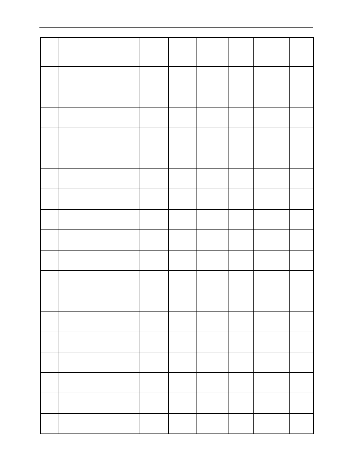
R&S CMU Test Report
Item
No.
Description
RX inherent spurious response at RF2,
f
= 454.02875 MHz,
IN
R&S CMU frequency = 300 MHz
RX inherent spurious response at RF2,
f
= 500 MHz,
IN
R&S CMU frequency = 505.35 MHz
RX inherent spurious response at RF2,
f
= 968.0575 MHz,
IN
R&S CMU frequency = 60 MHz
RX inherent spurious response at RF2,
f
= 1200 MHz,
IN
R&S CMU frequency = 291.9425 MHz
RX inherent spurious response at RF2,
f
= 645.3716667 MHz,
IN
R&S CMU frequency = 60 MHz
RX inherent spurious response at RF2,
f
= 1200 MHz,
IN
R&S CMU frequency = 891.9425 MHz
RX inherent spurious response at RF2,
f
= 1936.115 MHz,
IN
R&S CMU frequency = 60 MHz
RX inherent spurious response at RF2,
f
= 2200 MHz,
IN
R&S CMU frequency = 191.9425 MHz
RX inherent spurious response at RF2,
f
= 1226.97 MHz,
IN
R&S CMU frequency = 2200 MHz
RX inherent spurious response at RF2,
f
= 1821.4 MHz,
IN
R&S CMU frequency = 1800 MHz
RX inherent spurious response at RF2,
f
= 2936.17 MHz,
IN
R&S CMU frequency = 1250 MHz
RX inherent spurious response at RF2,
f
= 843.085 MHz,
IN
R&S CMU frequency = 2200 MHz
RX inherent spurious response at RF2,
f
= 421.5425 MHz,
IN
R&S CMU frequency = 2200 MHz
RX inherent spurious response at RF2,
f
= 281.0283333 MHz,
IN
R&S CMU frequency = 2200 MHz
RX inherent spurious response at RF2,
f
= 1816.115 MHz,
IN
R&S CMU frequency = 2200 MHz
RX inherent spurious response at RF2,
f
= 908.0575 MHz,
IN
R&S CMU frequency = 2200 MHz
RX inherent spurious response at RF2,
= 605.3716667 MHz,
f
IN
R&S CMU frequency = 2200 MHz
RX inherent spurious response at RF2,
= 1671.5425 MHz,
f
IN
R&S CMU frequency = 1250 MHz
Measure-
ment
to section
Min. Actual Max.
Measurement
uncertainty
Unit
–50 dBc
–50 dBc
–50 dBc
–50 dBc
–50 dBc
–50 dBc
–50 dBc
–50 dBc
–50 dBc
–50 dBc
–50 dBc
–50 dBc
–50 dBc
–50 dBc
–50 dBc
–50 dBc
–50 dBc
–50 dBc
1100.4903.82 1.33 E-5

Test Report R&S CMU
Item
No.
Description
RX inherent spurious response at RF2,
f
= 2200 MHz, R&S CMU frequency =
IN
1778.4575 MHz
RX inherent spurious response at RF2,
f
= 1812.056667 MHz,
IN
R&S CMU frequency = 1250 MHz
RX inherent spurious response at RF2,
f
= 1681.5425 MHz,
IN
R&S CMU frequency = 1680 MHz
RX inherent spurious response at RF2,
f
= 1468.085 MHz,
IN
R&S CMU frequency = 1250 MHz
RX inherent spurious response at RF2,
f
= 1683.085 MHz,
IN
R&S CMU frequency = 1680 MHz
RX inherent spurious response at RF2,
f
= 1943.085 MHz,
IN
R&S CMU frequency = 2200 MHz
RX inherent spurious response at RF2,
f
= 978.7233333 MHz,
IN
R&S CMU frequency = 1250 MHz
RX inherent spurious response at RF2,
f
= 1295.39 MHz,
IN
R&S CMU frequency = 2200 MHz
RX inherent spurious response at RF2,
f
= 1210.843333 MHz, R&S CMU
IN
frequency = 1210.743333 MHz
RX inherent spurious response at RF2,
f
= 1262.31375 MHz,
IN
R&S CMU frequency = 1260 MHz
RX inherent spurious response at RF4
IN, f
= 968.0575 MHz,
IN
R&S CMU frequency = 60 MHz
RX inherent spurious response at RF4
IN, f
= 1200 MHz,
IN
R&S CMU frequency = 291.9425 MHz
RX inherent spurious response at RF4
IN, f
= 645.3716667 MHz, R&S CMU
IN
frequency = 60 MHz
RX inherent spurious response at RF4
IN, f
= 1200 MHz,
IN
R&S CMU frequency = 891.9425 MHz
RX inherent spurious response at RF4
IN, f
= 1936.115 MHz,
IN
R&S CMU frequency = 60 MHz
RX inherent spurious response at RF4
IN, f
= 2200 MHz,
IN
R&S CMU frequency = 191.9425 MHz
RX inherent spurious response at RF4
= 1671.5425 MHz,
IN, f
IN
R&S CMU frequency = 1250 MHz
RX inherent spurious response at RF4
= 2200 MHz, R&S CMU
IN, f
IN
frequency = 1778.4575 MHz
Measure-
ment
to section
Min. Actual Max.
Measurement
uncertainty
Unit
–50 dBc
–50 dBc
–50 dBc
–50 dBc
–50 dBc
–50 dBc
–50 dBc
–50 dBc
–50 dBc
–50 dBc
–50 dBc
–50 dBc
–50 dBc
–50 dBc
–50 dBc
–50 dBc
–50 dBc
–50 dBc
1100.4903.82 1.34 E-5

R&S CMU Test Report
Item
No.
Description
RX inherent spurious response at RF4
IN, f
= 1812.056667 MHz,
IN
R&S CMU frequency = 1250 MHz
RX inherent spurious response at RF4
IN, f
= 1681.5425 MHz, R&S CMU
IN
frequency = 1680 MHz
RX inherent spurious response at RF4
IN, f
= 1468.085 MHz,
IN
R&S CMU frequency = 1250 MHz
RX inherent spurious response at RF4
IN, f
= 1683.085 MHz, R&S CMU
IN
frequency = 1680 MHz
RX inherent spurious response at RF4
IN, f
= 1943.085 MHz,
IN
R&S CMU frequency = 2200 MHz
RX inherent spurious response at RF4
IN, f
= 978.7233333 MHz, R&S CMU
IN
frequency = 1250 MHz
RX inherent spurious response at RF4
IN, f
= 1295.39 MHz,
IN
R&S CMU frequency = 2200 MHz
RX inherent spurious response at RF4
IN, f
= 1210.843333 MHz, R&S CMU
IN
frequency = 1210.743333 MHz
RX inherent spurious response at RF4
IN, f
= 1262.31375 MHz,
IN
R&S CMU frequency = 1260 MHz
Measure-
ment
to section
Min. Actual Max.
Measurement
uncertainty
Unit
–50 dBc
–50 dBc
–50 dBc
–50 dBc
–50 dBc
–50 dBc
–50 dBc
–50 dBc
–50 dBc
RX SSB Phase Noise
RX SSB phase noise at RF2
f = 100 MHz, f = +20 kHz
RX SSB phase noise at RF2
f = 100 MHz, f = +250 kHz
RX SSB phase noise at RF2
f = 100 MHz, f = +400 kHz
RX SSB phase noise at RF2
f = 100 MHz, f = +1990 kHz
RX SSB phase noise at RF2
f = 945 MHz, f = +20 kHz
RX SSB phase noise at RF2
f = 945 MHz, f = +250 kHz
RX SSB phase noise at RF2
f = 945 MHz, f = +400 kHz
RX SSB phase noise at RF2
f = 945 MHz, f = +1990 kHz
RX SSB phase noise at RF2
f = 1850 MHz, f = –20 kHz
RX SSB phase noise at RF2
f = 1850 MHz, f = -–250 kHz
RX SSB phase noise at RF2
f = 1850 MHz, f = -–400 kHz
RX SSB
–100
phase noise
–110
–118
–118
–100 dBc/Hz
–110 dBc/Hz
–118 dBc/Hz
–118 dBc/Hz
–100 dBc/Hz
–110 dBc/Hz
–118 dBc/Hz
1100.4903.82 1.35 E-5

Test Report R&S CMU
Item
No.
RX SSB phase noise at RF2
f = 1850 MHz, f = -–1990 kHz
RX SSB phase noise at RF2
f = 2200 MHz, f = –20 kHz
RX SSB phase noise at RF2
f = 2200 MHz, f = –250 kHz
RX SSB phase noise at RF2
f = 2200 MHz, f = –400 kHz
RX SSB phase noise at RF2
f = 2200 MHz, f = –1990 kHz
Description
RX Residual FM/AM
RX Residual FM at 500 MHz at RF4
IN, –20 dBm
30Hz to 15 kHz, rms
RX Residual FM at 500 MHz at RF4
IN, –20 dBm
30Hz to 15 kHz, peak
RX Residual FM at 500 MHz at RF4
IN, –20 dBm
CCITT, rms
RX Residual AM at 500 MHz at RF4
IN, –20 dBm
CCITT, rms
RX Residual FM at 900 MHz at RF4
IN, –20 dBm
30Hz to 15 kHz, rms
RX Residual FM at 900 MHz at RF4
IN, –20 dBm
30Hz to 15 kHz, peak
RX Residual FM at 900 MHz at RF4
IN, –20 dBm
CCITT, rms
RX Residual AM at 900 MHz at RF4
IN, –20 dBm
CCITT, rms
RX Residual FM at 1900 MHz at RF4
IN, –20 dBm
30Hz to 15 kHz, rms
RX Residual FM at 1900 MHz at RF4
IN, –20 dBm
30Hz to 15 kHz, peak
RX Residual FM at 1900 MHz at RF4
IN, –20 dBm
CCITT, rms
RX Residual AM at 1900 MHz at RF4
IN, –20 dBm
CCITT, rms
RX Residual FM at 2100 MHz at RF4
IN, –20 dBm
30Hz to 15 kHz, rms
Measure-
ment
to section
–118 dBc/Hz
–100 dBc/Hz
–110 dBc/Hz
–118 dBc/Hz
–118 dBc/Hz
RX residual
FM/AM
200 Hz
5 Hz
0.02 %
50 Hz
200 Hz
5 Hz
0.02 %
50 Hz
200 Hz
5 Hz
0.02 %
50 Hz
Min. Actual Max.
50 Hz
Measurement
uncertainty
Unit
1100.4903.82 1.36 E-5

R&S CMU Test Report
Item
No.
RX Residual FM at 2100 MHz at RF4
IN, –20 dBm
30Hz to 15 kHz, peak
RX Residual FM at 2100 MHz at RF4
IN, –20 dBm
CCITT, rms
RX Residual AM at 2100 MHz at RF4
IN, –20 dBm
CCITT, rms
RX Residual FM at 2500 MHz at RF4
IN, –20 dBm
30Hz to 15 kHz, rms
RX Residual FM at 2500 MHz at RF4
IN, –20 dBm
30Hz to 15 kHz, peak
RX Residual FM at 2500 MHz at RF4
IN, –20 dBm
CCITT, rms
RX Residual AM at 2500 MHz at RF4
IN, –20 dBm
CCITT, rms
Description
Measure-
ment
to section
200 Hz
5 Hz
0.02 %
50 Hz
200 Hz
5 Hz
0.02 %
Min. Actual Max.
Measurement
uncertainty
Unit
RX Average Noise Level
RX average noise level
RF1, RBW = 1 kHz,
expPow = 47 dBm, f = 10 MHz
RX average noise level
RF1, RBW = 1 kHz,
expPow = 47 dBm, f = 500 MHz
RX average noise level
RF1, RBW = 1 kHz,
expPow = 47 dBm, f = 1000 MHz
RX average noise level
RF1, RBW = 1 kHz,
expPow = 47 dBm, f = 1500 MHz
RX average noise level
RF1, RBW = 1 kHz,
expPow = 47 dBm, f = 2200 MHz
RX average noise level
RF1, RBW = 1 kHz,
expPow = 47 dBm, f = 2700 MHz
RX average noise level
RF1, RBW = 1 kHz,
expPow = 10 dBm, f = 10 MHz
RX average noise level
RF1, RBW = 1 kHz,
expPow = 10 dBm, f = 500 MHz
RX average noise level
RF1, RBW = 1 kHz,
expPow = 10 dBm, f = 1000 MHz
RX average noise level
RF1, RBW = 1 kHz,
expPow = 10 dBm, f = 1500 MHz
RX average
noise level
–100 dBc
–100 dBc
–100 dBc
–100 dBc
–95 dBc
–100 dBc
–100 dBc
–100 dBc
–100 dBc
–100 dBc
1100.4903.82 1.37 E-5

Test Report R&S CMU
Item
No.
RX average noise level
RF1, RBW = 1 kHz,
expPow = 10 dBm, f = 2200 MHz
RX average noise level
RF1, RBW = 1 kHz,
expPow = 10 dBm, f = 2700 MHz
RX average noise level
RF2, RBW = 500 kHz,
expPow = 33 dBm, f = 10 MHz
RX average noise level
RF2, RBW = 500 kHz,
expPow = 33 dBm, f = 500 MHz
RX average noise level
RF2, RBW = 500 kHz,
expPow = 33 dBm, f = 1000 MHz
RX average noise level
RF2, RBW = 500 kHz,
expPow = 33 dBm, f = 1500 MHz
RX average noise level
RF2, RBW = 500 kHz,
expPow = 33 dBm, f = 2200 MHz
RX average noise level
RF2, RBW = 500 kHz,
expPow = 33 dBm, f = 2700 MHz
RX average noise level
RF2, RBW = 500 kHz,
expPow = –4 dBm, f = 10 MHz
RX average noise level
RF2, RBW = 500 kHz,
expPow = –4 dBm, f = 500 MHz
RX average noise level
RF2, RBW = 500 kHz,
expPow = –4 dBm, f = 1000 MHz
RX average noise level
RF2, RBW = 500 kHz,
expPow = –4 dBm, f = 1500 MHz
RX average noise level
RF2, RBW = 500 kHz,
expPow = –4 dBm, f = 2200 MHz
RX average noise level
RF2, RBW = 500 kHz,
expPow = –4 dBm, f = 2700 MHz
RX average noise level
RF4 IN, RBW = 1 kHz,
expPow = –22 dBm, f = 10 MHz
RX average noise level
RF4 IN, RBW = 1 kHz,
expPow = 0 dBm, f = 500 MHz
RX average noise level
RF4 IN, RBW = 1 kHz,
expPow = 0 dBm, f = 1000 MHz
RX average noise level
RF4 IN, RBW = 1 kHz,
expPow = 0 dBm, f = 1500 MHz
Description
Measure-
ment
to section
–100 dBc
–95 dBc
–73 dBc
–73 dBc
–73 dBc
–73 dBc
–73 dBc
–68 dBc
–73 dBc
–73 dBc
–73 dBc
–73 dBc
–73 dBc
–68 dBc
–100 dBc
–100 dBc
–100 dBc
–100 dBc
Min. Actual Max.
Measurement
uncertainty
Unit
1100.4903.82 1.38 E-5

R&S CMU Test Report
Item
No.
RX average noise level
RF4 IN, RBW = 1 kHz,
expPow = 0 dBm, f = 2200 MHz
RX average noise level
RF4 IN, RBW = 1 kHz,
expPow = 0 dBm, f = 2700 MHz
RX average noise level
RF4 IN, RBW = 1 kHz,
expPow = –22 dBm, f = 10 MHz
RX average noise level
RF4 IN, RBW = 1 kHz,
expPow = –22 dBm, f = 500 MHz
RX average noise level
RF4 IN, RBW = 1 kHz,
expPow = –22 dBm, f = 1000 MHz
RX average noise level
RF4 IN, RBW = 1 kHz,
expPow = –22 dBm, f = 1500 MHz
RX average noise level
RF4 IN, RBW = 1 kHz,
expPow = –22 dBm, f = 2200 MHz
RX average noise level
RF4 IN, RBW = 1 kHz,
expPow = –22 dBm, f = 2700 MHz
Description
Measure-
ment
to section
–100 dBc
–95 dBc
–100 dBc
–100 dBc
–100 dBc
–100 dBc
–100 dBc
–95 dBc
Min. Actual Max.
Measurement
uncertainty
Unit
1100.4903.82 1.39 E-5
Test Report R&S CMU
TX Generator level error at RF1 (measurement on frequency cal. points)
Frequency
MHz
Level
in dBm
Tolerance See data sheet:
TX Generator level error at RF2 (measurement on frequency cal. points)
Frequency
MHz
Level
in dBm
Tolerance See data sheet:
TX Generator level error at RF3 OUT (measurement on frequency cal. points)
Frequency
MHz
Level
in dBm
Tolerance See data sheet:
10, 100, 200, 300, 400, 500, 600, 700, 800, 1000,
1100, 1200, 1300, 1400, 1500, 1600, 1700, , 2100,
2200, 2300, 2400, 2500, 2600, 2700
–33, –55, –73, –87, –106, –117, –130 –33, –55, –73, –87, –106, –117, –130
Base Unit RF Generator
10, 100, 200, 300, 400, 500, 600, 700, 800, 1000,
1100, 1200, 1300, 1400, 1500, 1600, 1700, , 2100,
2200, 2300, 2400, 2500, 2600, 2700
–16, –41, –59, –73, –95, –106, –117 –16, –41, –59, –73, –95, –106, –117
Base Unit RF Generator
10, 100, 200, 300, 400, 500, 600, 700, 800, 1000,
1100, 1200, 1300, 1400, 1500, 1600, 1700, , 2100,
2200, 2300, 2400, 2500, 2600, 2700
+5, –18, –36, –50, –72, –80, –90 +5, –18, –36, –50, –72, –80, –90
Base Unit RF Generator
820, 840, 860, 880, 900, 920, 940, 960, 1710, 1730,
1750, 1770, 1790, 1810, 1830, 1850, 1870, 1890, 1910,
1930, 1950, 1970, 1990
See data sheet:
GSM Specification RF Generator
820, 840, 860, 880, 900, 920, 940, 960, 1710, 1730,
1750, 1770, 1790, 1810, 1830, 1850, 1870, 1890, 1910,
1930, 1950, 1970, 1990
See data sheet:
GSM Specification RF Generator
820, 840, 860, 880, 900, 920, 940, 960, 1710, 1730,
1750, 1770, 1790, 1810, 1830, 1850, 1870, 1890, 1910,
1930, 1950, 1970, 1990
See data sheet:
GSM Specification RF Generator
RX Power meter (frequency selective) level error at RF1 (measurement on frequency cal. points)
Frequency
in MHz
Level
in dBm
Tolerance See data sheet:
RX Power meter (frequency selective) level error at RF2 (measurement on frequency cal. points)
Frequency
in MHz
Level
in dBm
Tolerance See data sheet:
50, 100, 200, 300, 400, 500, 600, 700, 800, 1000,
1100, 1200, 1300, 1400, 1500, 1600, 1700, , 2000,
2100, 2200, 2300, 2400, 2500, 2600, 2700
+47, +40, +33, +30, +25, +20, +15, +10, +6, 0, –5,
–10, –15, –20, - 25, –30, –35, –40
Note: P = –40 dBm is valid for f = 50 MHz to 2200
MHz only
Base Unit RF Analyzer
50, 100, 200, 300, 400, 500, 600, 700, 800, 1000,
1100, 1200, 1300, 1400, 1500, 1600, 1700, , 2000,
2100, 2200, 2300, 2400, 2500, 2600, 2700
+33, +26, +19, +16, +11, +6, +1, –4, –8, –14, –19,
–24, - 29, –34, –39, –44, –49, –54
Note: P = –54 dBm is valid for f = 50 MHz to
2200 MHz only
Base Unit RF Analyzer
450, 470, 490, 820, 840, 860, 880, 900, 920, 940, 960,
1720, 1740, 1760, 1780, 1800, 1820, 1840, 1860, 1880,
1900, 1920, 1940, 1960, 1980
+47, +40, +33, +30, +25, +20, +15, +10, +6, 0, –5, –10,
–15, –20, - 25, –30, –35, –40
Note: P = –40 dBm is valid for f = 50 MHz to 2200 MHz
only
See data sheet:
GSM Specification RF Analyzer
450, 470, 490, 820, 840, 860, 880, 900, 920, 940, 960,
1720, 1740, 1760, 1780, 1800, 1820, 1840, 1860, 1880,
1900, 1920, 1940, 1960, 1980
+33, +26, +19, +16, +11, +6, +1, –4, –8, –14, –19, –24,
–29, –34, –39, –44, –49, –54
Note: P = –54 dBm is valid for f = 50 MHz to 2200 MHz
only
See data sheet:
GSM Specification RF Analyzer
1100.4903.82 1.40 E-5

R&S CMU Test Report
RX Power meter (frequency selective) level error at RF4 IN
(measurement on frequency cal. points)
Frequency
in MHz
Level
in dBm
Tolerance See data sheet:
RX Power meter (wideband) level error at RF1 (measurement on frequency cal. points)
Frequency
in MHz
Level
in dBm
Tolerance See data sheet:
50, 100, 200, 300, 400, 500, 600, 700, 800, 1000,
1100, 1200, 1300, 1400, 1500, 1600, 1700, , 2000,
2100, 2200, 2300, 2400, 2500, 2600, 2700
0, –6, –9, –14, –19, –24, –29, –33, –39, –44, –49,
–54, –59, –64, –69, –74, –80
Note: P = –80 dBm is valid for f = 50 MHz to
2200 MHz only
Base Unit RF Analyzer
50, 100, 200, 300, 400, 500, 600, 700, 800, 1000,
1100, 1200, 1300, 1400, 1500, 1600, 1700, , 2000,
2100, 2200, 2300, 2400, 2500, 2600, 2700
+47, +40, +33, +30, +25, +20, +15, +10
Note: P> +33 dBm is calibrated from 800 MHz to
2000 MHz only;
Base Unit RF Analyzer
450, 470, 490, 820, 840, 860, 880, 900, 920, 940, 960,
1720, 1740, 1760, 1780, 1800, 1820, 1840, 1860, 1880,
1900, 1920, 1940, 1960, 1980
0, –6, –9, –14, –19, –24, –29, –33, –39, –44, –49, –54,
–59, –4, –69, –74, –80
Note: P = –80 dBm is valid for f = 50 MHz to 2200 MHz
only
See data sheet:
GSM Specification RF Analyzer
450, 470, 490, 820, 840, 860, 880, 900, 920, 940, 960,
1720, 1740, 1760, 1780, 1800, 1820, 1840, 1860, 1880,
1900, 1920, 1940, 1960, 1980
+47, +40, +33, +30, +25, +20, +15, +10
Note: P> +33 dBm is calibrated from 800 MHz to
2000 MHz only;
See data sheet:
Base Unit RF Analyzer
RX Power meter (wideband) level error at RF2 (measurement on frequency cal. points)
Frequency
in MHz
Level
in dBm
Tolerance See data sheet:
RX Power meter (wideband) level error at RF4 IN (measurement on frequency cal. points)
Frequency
in MHz
Level
in dBm
Tolerance See data sheet:
50, 100, 200, 300, 400, 500, 600, 700, 800, 1000,
1100, 1200, 1300, 1400, 1500, 1600, 1700, , 2000,
2100, 2200, 2300, 2400, 2500, 2600, 2700
+33, +26, +19, +16, +11, +6, +1, –4 +33, +26, +19, +16, +11, +6, +1, –4
Base Unit RF Analyzer
50, 100, 200, 300, 400, 500, 600, 700, 800, 1000,
1100, 1200, 1300, 1400, 1500, 1600, 1700, , 2000,
2100, 2200, 2300, 2400, 2500, 2600, 2700
0, –6, –9, –14, –19, –24, –29 0, –6, –9, –14, –19, –24, –29
Base Unit RF Analyzer
450, 470, 490, 820, 840, 860, 880, 900, 920, 940, 960,
1720, 1740, 1760, 1780, 1800, 1820, 1840, 1860, 1880,
1900, 1920, 1940, 1960, 1980
See data sheet:
Base Unit RF Analyzer
450, 470, 490, 820, 840, 860, 880, 900, 920, 940, 960,
1720, 1740, 1760, 1780, 1800, 1820, 1840, 1860, 1880,
1900, 1920, 1940, 1960, 1980
See data sheet:
Base Unit RF Analyzer
1100.4903.82 1.41 E-5

Test Report R&S CMU
Options for R&S CMU200: R&S CMU-K20, K21, K22, K23, K24, TX Generator GSM Modulation
Output RF3 OUT, level 10 dBm, GSM Non Signaling
Training Sequence GSM0, Bit Modulation PRBS, Transmission Burst
Item
No.
K20 TX GSM phase error
at 460 MHz, peak
K20 TX GSM phase error
at 460 MHz, rms
K20 TX GSM frequency error
at 460 MHz
K20 TX GSM phase error
at 496 MHz, peak
K20 TX GSM phase error
at 496 MHz, rms
K20 TX GSM frequency error
at 496 MHz
K21 TX GSM phase error
at 921 MHz, peak
K21 TX GSM phase error
at 921 MHz, rms
K21 TX GSM frequncy error
at 921 MHz
K21 TX GSM phase error
at 960 MHz, peak
K21 TX GSM phase error
at 960 MHz, rms
K21 TX GSM frequency error
at 960 MHz
K22 TX GSM phase error
at 1805 MHz, peak
K22 TX GSM phase error
at 1805 MHz, rms
K22 TX GSM frequency error
at 1805 MHz
K22 TX GSM phase error
at 1880 MHz, peak
K22 TX GSM phase error
at 1880 MHz, rms
K22 TX GSM frequency error
at 1880 MHz
K23 TX GSM phase error
at 1930 MHz, peak
K23 TX GSM phase error
at 1930 MHz, rms
K23 TX GSM frequency error
at 1930 MHz
K23 TX GSM phase error
at 1990 MHz, peak
Description
Measurement
to section
GSM
Modulation
–1 +1 °
–15 +15 Hz
–4 +4 °
–1 +1 °
–15 +15 Hz
–4 +4 °
–1 +1 °
–15 +15 Hz
–4 +4 °
–1 +1 °
–15 +15 Hz
–4 +4 °
–1 14 °
–15 +15 Hz
–4 +4 °
–1 +1 °
–15 +15 Hz
–4 +4 °
–1 +1 °
–15 +15 Hz
–4 +4 °
Min. Actual Max.
–4 +4 °
Measurement
uncertainty
Unit
1100.4903.82 1.42 E-5
R&S CMU Test Report
Item
No.
K23 TX GSM phase error
at 1990 MHz, rms
K23 TX GSM frequency error
at 1990 MHz
K24 TX GSM phase error
at 869 MHz, peak
K24 TX GSM phase error
at 869 MHz, rms
K24 TX GSM frequency error
at 869 MHz
K24 TX GSM phase error
at 894 MHz, peak
K24 TX GSM phase error
at 894 MHz, rms
K24 TX GSM frequency error
at 894 MHz
Description
Measurement
to section
–1 +1 °
–15 +15 Hz
–4 +4 °
–1 +1 °
–15 +15 Hz
–4 +4 °
–1 +1 °
–15 +15 Hz
Min. Actual Max.
Measurement
uncertainty
Unit
Options for R&S CMU200: R&S CMU-K20, K21, K22, K23, K24, RX Analyzer GSM Demodulation
Input RF2, GSM Non Signaling
Training Sequence GSM0, Trigger Source IF Power, Trigger Level Medium
Item
No.
K20 GSM phase error RX
at 450 MHz, peak, level +5 dBm
K20 RX GSM phase error
at 450 MHz, rms, level +5 dBm
K20 RX GSM frequency error
at 450 MHz, level +5 dBm
K20 RX GSM phase error
at 486 MHz, peak, level –14 dBm
K20 RX GSM phase error
at 486 MHz, rms, level –14 dBm
K20 RX GSM frequency error
at 486 MHz, level –14 dBm
K21 RX GSM phase error
at 876 MHz, peak, level +5 dBm
K21 RX GSM phase error
at 876 MHz, rms, level +5 dBm
K21 RX GSM frequency error
at 876 MHz, level +5 dBm
K21 RX GSM phase error
at 915 MHz, peak, level –14 dBm
K21 RX GSM phase error
at 915 MHz, rms, level –14 dBm
Description
Measurement
to section
RX
Demodulation
–0.6 +0.6 °
–10 +10 Hz
–2 +2 °
–0.6 +0.6 °
–10 +10 Hz
RX
Demodulation
–0.6 +0.6 °
–10 +10 Hz
–2 +2 °
–0.6 +0.6 °
Min. Actual Max.
–2 +2 °
–2 +2 °
Measurement
uncertainty
Unit
1100.4903.82 1.43 E-5

Test Report R&S CMU
Item
No.
K21 RX GSM frequency error
at 915 MHz, level –14 dBm
K22 RX GSM phase error
at 1710 MHz, peak, level +5 dBm
K22 RX GSM phase error
at 1710 MHz, rms, level +5 dBm
K22 RX GSM frequency error
at 1710 MHz, level +5 dBm
K22 RX GSM phase error
at 1785 MHz, peak, level –14 dBm
K22 RX GSM phase error
at 1785 MHz, rms, level –14 dBm
K22 RX GSM frequency error
at 1785 MHz, level –14 dBm
K23 RX GSM phase error
at 1850 MHz, peak, level +5 dBm
K23 RX GSM phase error
at 1850 MHz, rms, level +5 dBm
K23 RX GSM frequency error
at 1850 MHz, level +5 dBm
K23 RX GSM phase error
at 1910 MHz, peak, level –14 dBm
K23 RX GSM phase error
at 1910 MHz, rms, level –14 dBm
K23 RX GSM frequency error
at 1910 MHz, level –14 dBm
K24 RX GSM phase error
at 824 MHz, peak, level +5 dBm
K24 RX GSM phase error
at 824 MHz, rms, level +5 dBm
K24 RX GSM frequency error
at 824 MHz, level +5 dBm
K24 RX GSM phase error
at 849 MHz, peak, level –14 dBm
K24 RX GSM phase error
at 849 MHz, rms, level –14 dBm
K24 RX GSM frequency error
at 849 MHz, level –14 dBm
Description
Measurement
to section
–10 +10 Hz
RX
Demodulation
–0.6 +0.6 °
–10 +10 Hz
–2 +2 °
–0.6 +0.6 °
–10 +10 Hz
RX
Demodulation
–0.6 +0.6 °
–10 +10 Hz
–2 +2 °
–0.6 +0.6 °
–10 +10 Hz
RX
Demodulation
–0.6 +0.6 °
–10 +10 Hz
–2 +2
–0.6 +0.6
–10 +10 Hz
Min. Actual Max.
–2 +2 °
–2 +2 °
–2 +2 °
Measurement
uncertainty
Unit
1100.4903.82 1.44 E-5

R&S CMU Test Report
Options for R&S CMU200: R&S CMU-K83, K84, K85, K86, TX Generator CDMA2000 Modulation
Item
No.
K83 TX CDMA2000 rho factor
at 460 MHz
K83 TX CDMA2000 carrier
suppression
at 460 MHz
K83 TX CDMA2000 rho factor
at 493.48 MHz
K83 TX CDMA2000 carrier
suppression
at 493.48 MHz
K84 TX CDMA2000 rho factor
at 870.03 MHz
K84 TX CDMA2000 carrier
suppression
at 870.03 MHz
K84 TX CDMA2000 rho factor
at 893.31 MHz
K84 TX CDMA2000 carrier
suppression
at 893.31 MHz
K85 TX CDMA2000 rho factor
at 1930.05 MHz
K85 TX CDMA2000 carrier
suppression
at 1930.05 MHz
K85 TX CDMA2000 rho factor
at 1989.95 MHz
K85 TX CDMA2000 carrier
suppression
at 1989.95 MHz
K86 TX CDMA2000 rho factor
at 2110 MHz
K86 TX CDMA2000 carrier
suppression
at 2110 MHz
K86 TX CDMA2000 rho factor
at 2169.95 MHz
K86 TX CDMA2000 carrier
suppression
at 2169.95 MHz
Description
Measurement
to section
TX
CDMA2000
Modulation
35 dB
TX
CDMA2000
Modulation
35 dB
TX
CDMA2000
Modulation
35 dB
TX
CDMA2000
Modulation
35 dB
TX
CDMA2000
Modulation
35 dB
TX
CDMA2000
Modulation
35 dB
TX
CDMA2000
Modulation
35 dB
TX
CDMA2000
Modulation
35 dB
Min. Actual Max.
0.985
0.985
0.985
0.985
0.985
0.985
0.985
0.985
Measurement
uncertainty
Unit
1100.4903.82 1.45 E-5

Test Report R&S CMU
Options for R&S CMU200: R&S CMU-K83, K84, K85, K86, RX Analyzer CDMA2000 Demodulation
Item
No.
K83 RX CDMA2000 waveform quality
at 450 MHz
K83 RX CDMA2000 frequency
measurement error
at 450 MHz
K83 RX CDMA2000 waveform quality
at 483.480 MHz
K83 RX CDMA2000 frequency
measurement error
at 483.480 MHz
K84 RX CDMA2000 waveform quality
at 825.030 MHz
K84 RX CDMA2000 frequency
measurement error
at 825.030 MHz
K84 RX CDMA2000 waveform quality
at 848.310 MHz
K84 RX CDMA2000 frequency
measurement error
at 848.310 MHz
K85 RX CDMA2000 waveform quality
at 1850.05 MHz
K85 RX CDMA2000 frequency
measurement error
at 1850.05 MHz
K85 RX CDMA2000 waveform quality
at 1909.950 MHz
K85 RX CDMA2000 frequency
measurement error
at 1909.950 MHz
K86 RX CDMA2000 waveform quality
at 1920.00 MHz
K86 RX CDMA2000 frequency
measurement error
at 1920.00 MHz
K86 RX CDMA2000 waveform quality
at 1979.950 MHz
K86 RX CDMA2000 frequency
measurement error
at 1979.950 MHz
Description
Measurement
to section
RX
CDMA2000
Demodulation
RX
CDMA2000
Demodulation
RX
CDMA2000
Demodulation
RX
CDMA2000
Demodulation
RX
CDMA2000
Demodulation
RX
CDMA2000
Demodulation
RX
CDMA2000
Demodulation
RX
CDMA2000
Demodulation
RX
CDMA2000
Demodulation
RX
CDMA2000
Demodulation
RX
CDMA2000
Demodulation
RX
CDMA2000
Demodulation
RX
CDMA2000
Demodulation
RX
CDMA2000
Demodulation
RX
CDMA2000
Demodulation
RX
CDMA2000
Demodulation
Measurement
Min. Actual Max.
0.9965
-30 +30 Hz
0.9965
-30 +30 Hz
0.9965
-30 +30 Hz
0.9965
-30 +30 Hz
0.9965
-30 +30 Hz
0.9965
-30 +30 Hz
0.9965
-30 +30 Hz
0.9965
-30 +30 Hz
uncertainty
Unit
1100.4903.82 1.46 E-5

R&S CMU Test Report
Options for R&S CMU200: R&S CMU-K66, TX Generator WCDMA Modulation
Item
No.
K66 TX WCDMA global EVM rms
at 2110 MHz, level -46 dBm, RF2,
12.2kbps
K66 TX WCDMA global EVM rms
at 2170 MHz, level -46dBm, RF2,
12.2kbps
K66 TX WCDMA global EVM rms
at 2110 MHz, level -23 dBm,
RF3OUT, 12.2kbps
K66 TX WCDMA global EVM rms
at 2170 MHz, level -23 dBm,
RF3OUT, 12.2kbps
K66 TX WCDMA global EVM rms
at 2110 MHz, level -46 dBm, RF2,
384kbps
K66 TX WCDMA global EVM rms
at 2170 MHz, level -46 dBm, RF2,
384kbps
K66 TX WCDMA global EVM rms
at 2110 MHz, level -23 dBm,
RF3OUT, 384kbps
K66 TX WCDMA global EVM rms
at 2170 MHz, level -23 dBm,
RF3OUT, 384kbps
Description
Measurement
to section
TX WCDMA
Modulation
TX WCDMA
Modulation
TX WCDMA
Modulation
TX WCDMA
Modulation
TX WCDMA
Modulation
TX WCDMA
Modulation
TX WCDMA
Modulation
TX WCDMA
Modulation
Measurement
Min. Actual Max.
8.0 %
8.0 %
8.0 %
8.0 %
8.0 %
8.0 %
8.0 %
8.0 %
uncertainty
Unit
1100.4903.82 1.47 E-5

Test Report R&S CMU
Options for R&S CR&S MU200: R&S CMU-K65 RX Analyzer WCDMA Demodulation
Item
No.
K65 RX WCDMA EVM rms
at 1920 MHz, Max level +25dBm,
input level +10dBm, RF 2
K65 RX WCDMA I/Q Origin Offset
at 1920 MHz, Max level +25 dBm,
input level +10dBm, RF 2
K65 RX WCDMA I/Q Imbalance
at 1920 MHz, Max level +25 dBm,
input level +10dBm, RF 2
K65 RX WCDMA Carrier frequency
error
at 1920 MHz, Max level +25 dBm,
input level +10dBm, RF 2
K65 RX WCDMA Peak code domain
error
at 1920 MHz, Max level +25 dBm,
input level +10dBm, RF 2
K65 RX WCDMA EVM rms
at 1980 MHz, Max level +25 dBm,
input level +10dBm, RF 2
K65 RX WCDMA I/Q Origin Offset
at 1980 MHz, Max level +25 dBm,
input level +10dBm, RF 2
K65 RX WCDMA I/Q Imbalance
at 1980 MHz, Max level +25 dBm,
input level +10dBm, RF 2
K65 RX WCDMA Carrier frequency
error
at 1980 MHz, Max level +25 dBm,
input level +10dBm, RF 2
K65 RX WCDMA Peak code domain
error
at 1980 MHz, Max level +25 dBm,
input level +10dBm, RF 2
K65 RX WCDMA EVM rms
at 1920 MHz, Max level +25 dBm,
input level +10dBm, RF 2
K65 RX WCDMA I/Q Origin Offset
at 1920 MHz, Max level +9 dBm,
input level +5dBm, RF 2
K65 RX WCDMA I/Q Imbalance
at 1920 MHz, Max level +9 dBm,
input level +5dBm, RF 2
K65 RX WCDMA Carrier frequency
error
at 1920 MHz, Max level +9 dBm,
input level +5dBm, RF 2
K65 RX WCDMA Peak code domain
error
at 1920 MHz, Max level +9 dBm,
input level +5dBm, RF 2
Description
Measurement
to section
RX WCDMA
Demodulation
RX WCDMA
Demodulation
RX WCDMA
Demodulation
RX WCDMA
Demodulation
RX WCDMA
Demodulation
RX WCDMA
Demodulation
RX WCDMA
Demodulation
RX WCDMA
Demodulation
RX WCDMA
Demodulation
RX WCDMA
Demodulation
RX WCDMA
Demodulation
RX WCDMA
Demodulation
RX WCDMA
Demodulation
RX WCDMA
Demodulation
RX WCDMA
Demodulation
Measurement
Min. Actual Max.
2.5 %
-55 dB
-30 dB
-10 10 Hz
-40 dB
2.5 %
-55 dB
-30 dB
-10 10 Hz
-40 dB
2.5 %
-55 dB
-30 dB
-10 10 Hz
-40 dB
uncertainty
Unit
1100.4903.82 1.48 E-5

R&S CMU Test Report
Item
No.
K65 RX WCDMA EVM rms
at 1980 MHz, Max level +25dBm,
input level +10dBm, RF 2
K65 RX WCDMA I/Q Origin Offset
at 1980 MHz, Max level +9dBm,
input level +5dBm, RF 2
K65 RX WCDMA I/Q Imbalance
at 1980 MHz, Max level +9dBm,
input level +5dBm, RF 2
K65 RX WCDMA Carrier frequency
error
at 1980 MHz, Max level +9dBm,
input level +5dBm, RF 2
K65 RX WCDMA Peak code domain
error
at 1980 MHz, Max level +9dBm,
input level +5dBm, RF 2
K65 RX WCDMA EVM rms
at 1920 MHz, Max level +25dBm,
input level +10dBm, RF 2
K65 RX WCDMA I/Q Origin Offset
at 1920 MHz, Max level -14dBm,
input level -20dBm, RF 2
K65 RX WCDMA I/Q Imbalance
at 1920 MHz, Max level -14dBm,
input level -20dBm, RF 2
K65 RX WCDMA Carrier frequency
error
at 1920 MHz, Max level -14dBm,
input level -20dBm, RF 2
K65 RX WCDMA Peak code domain
error
at 1920 MHz, Max level -14dBm,
input level -20dBm, RF 2
K65 RX WCDMA EVM rms
at 1980 MHz, Max level +25dBm,
input level +10dBm, RF 2
K65 RX WCDMA I/Q Origin Offset
at 1980 MHz, Max level -14dBm,
input level -20dBm, RF 2
K65 RX WCDMA I/Q Imbalance
at 1980 MHz, Max level -14dBm,
input level -20dBm, RF 2
K65 RX WCDMA Carrier frequency
error
at 1980 MHz, Max level -14dBm,
input level -20dBm, RF 2
K65 RX WCDMA Peak code domain
error
at 1980 MHz, Max level -14dBm,
input level -20dBm, RF 2
K65 RX WCDMA EVM rms
at 1920 MHz, Max level 0dBm,
input level -5dBm, RF 4 IN
Description
Measurement
to section
RX WCDMA
Demodulation
RX WCDMA
Demodulation
RX WCDMA
Demodulation
RX WCDMA
Demodulation
RX WCDMA
Demodulation
RX WCDMA
Demodulation
RX WCDMA
Demodulation
RX WCDMA
Demodulation
RX WCDMA
Demodulation
RX WCDMA
Demodulation
RX WCDMA
Demodulation
RX WCDMA
Demodulation
RX WCDMA
Demodulation
RX WCDMA
Demodulation
RX WCDMA
Demodulation
RX WCDMA
Demodulation
Measurement
Min. Actual Max.
2.5 %
-55 dB
-30 dB
-10 10 Hz
-40 dB
2.5 %
-55 dB
-30 dB
-10 10 Hz
-40 dB
2.5 %
-55 dB
-30 dB
-10 10 Hz
-40 dB
2.5 %
uncertainty
Unit
1100.4903.82 1.49 E-5

Test Report R&S CMU
Item
No.
K65 RX WCDMA I/Q Origin Offset
at 1920 MHz, Max level 0dBm,
input level -5 dBm, RF 4 IN
K65 RX WCDMA I/Q Imbalance
at 1920 MHz, Max level 0dBm,
input level -5 dBm, RF 4 IN
K65 RX WCDMA Carrier frequency
error
at 1920 MHz, Max level 0dBm,
input level -5 dBm, RF 4 IN
K65 RX WCDMA Peak code domain
error
at 1920 MHz, Max level 0dBm,
input level -5 dBm, RF 4 IN
K65 RX WCDMA EVM rms
at 1980 MHz, Max level 0dBm,
input level -5 dBm, RF 4 IN
K65 RX WCDMA I/Q Origin Offset
at 1980 MHz, Max level 0dBm,
input level -5 dBm, RF 4 IN
K65 RX WCDMA I/Q Imbalance
at 1980 MHz, Max level 0dBm,
input level -5 dBm, RF 4 IN
K65 RX WCDMA Carrier frequency
error
at 1980 MHz, Max level 0dBm,
input level -5 dBm, RF 4 IN
K65 RX WCDMA Peak code domain
error
at 1980 MHz, Max level 0dBm,
input level -5 dBm, RF 4 IN
K65 RX WCDMA EVM rms
at 1920 MHz, Max level -37dBm,
input level -50 dBm, RF 4 IN
K65 RX WCDMA I/Q Origin Offset
at 1920 MHz, Max level -37dBm,
input level -50 dBm, RF 4 IN
K65 RX WCDMA I/Q Imbalance
at 1920 MHz, Max level -37dBm,
input level -50 dBm, RF 4 IN
K65 RX WCDMA Carrier frequency
error
at 1920 MHz, Max level -37dBm,
input level -50 dBm, RF 4 IN
K65 RX WCDMA Peak code domain
error
at 1920 MHz, Max level -37dBm,
input level -50 dBm, RF 4 IN
K65 RX WCDMA EVM rms
at 1980 MHz, Max level -37dBm,
input level -50 dBm, RF 4 IN
K65 RX WCDMA I/Q Origin Offset
at 1980 MHz, Max level -37dBm,
input level -50 dBm, RF 4 IN
Description
Measurement
to section
RX WCDMA
Demodulation
RX WCDMA
Demodulation
RX WCDMA
Demodulation
RX WCDMA
Demodulation
RX WCDMA
Demodulation
RX WCDMA
Demodulation
RX WCDMA
Demodulation
RX WCDMA
Demodulation
RX WCDMA
Demodulation
RX WCDMA
Demodulation
RX WCDMA
Demodulation
RX WCDMA
Demodulation
RX WCDMA
Demodulation
RX WCDMA
Demodulation
RX WCDMA
Demodulation
RX WCDMA
Demodulation
Measurement
Min. Actual Max.
-55 dB
-30 dB
-10 10 Hz
-40 dB
2.5 %
-55 dB
-30 dB
-10 10 Hz
-40 dB
2.5 %
-55 dB
-30 dB
-10 10 Hz
-40 dB
2.5 %
-55 dB
uncertainty
Unit
1100.4903.82 1.50 E-5

R&S CMU Test Report
Item
No.
K65 RX WCDMA I/Q Imbalance
at 1980 MHz, Max level -37dBm,
input level -50dBm, RF 4 IN
K65 RX WCDMA Carrier frequency
error
at 1980 MHz, Max level -37dBm,
input level -50dBm, RF 4 IN
K65 RX WCDMA Peak code domain
error
at 1980 MHz, Max level -37dBm,
input level -50 dBm, RF 4 IN
Description
Measurement
to section
RX WCDMA
Demodulation
RX WCDMA
Demodulation
RX WCDMA
Demodulation
Measurement
Min. Actual Max.
-30 dB
-10 10 Hz
-40 dB
uncertainty
Unit
1100.4903.82 1.51 E-5


Manual Adjustment R&S CMU
2 Adjustment
The following chapter describes the manual adjustment of the reference sources as well as the
software-controlled adjustment of individual module data after module replacement (automatic
adjustment of module data).
The manual adjustment of the +5 VDC reference source which provides the highly stable DC reference
voltage for the individual R&S CMU modules as well as that of the 10 MHz reference frequency source
which determines the frequency accuracy of the R&S CMU are described. The adjustment permits to
maintain and restore the data integrity of the instrument.
Manual adjustments must be performed at an ambient temperature between +23°C and +26°C after the
instrument has warmed up.
After the software-controlled adjustment has been performed, the R&S CMU is ready for use and offers
full data integrity except for the level accuracy. In order to attain the level accuracy specified in the data
sheet, it is necessary to record the path error data. To this end, the R&S CMU must be tested using the
test system ACS 100 (see chapter 1, Performance Test).
Manual Adjustment
In the following, the measuring instruments and auxiliary means required for the manual adjustment of
the R&S CMU , the appropriate preparations of the instrument as well as the individual adjustments will
be explained.
Measuring Instruments and Auxiliary Equipment
Table 2-1 Measuring instruments and auxiliary equipment for manual adjustment of the R&S CMU
Item Type of
instrument
1 Voltmeter DC measurement R&S URE3 350.5315.03
2 Spectrum analyzer
with
frequency counter
Required
characteristics
Frequency measurement up to 1 GHz
Appropriate device R & S order
number
R&S FSE 1066.3010.20 (30)
Use
page
1100.4903.82 2.1 E-5

R&S CMU Manual Adjustment
Preparing the Instrument
Opening the casing:
Note:
Remove the power plug on the R&S CMU and place the R&S
CMU onto the front handles.
Loosen the four Phillips screws at the four rear-panel feet and
take off the feet.
Pull off the instrument tube towards the top.
Locate the adjustment devices (see chapter 5, drawing
1100.0008.01 D page 3).
After performing the manual adjustment, close the casing again
in the reverse order.
If only the Option OCXO REFERENCE OSC. R&S CMU -B11/B12 is
to be adjusted, it is not necessary to open the complete tube of the
R&S CMU . The adjustment can be made from outside through the
ventilation holes using a small screwdriver (see chapter 5, drawing
1100.0008.01 D page 3).
Adjusting the + 5 VDC Reference Voltage
Preparation:
Adjustment:
Connect the DC voltmeter test cable to the SMB plug X221 (see
chapter 5, drawing 1100.1027.01 page 1) on the motherboard.
Switch on the R&S CMU and allow it to warm up for approx. 5
minutes.
Use potentiometer R120 on the REFERENCE BOARD to adjust
the measured value at the DC voltmeter to + 5.000 V ± 1 mV.
1100.4903.82 2.2 E-5

Manual Adjustment R&S CMU
For the measurement at connector RF3 OUT set the generator to
Adjusting the 10 MHz Reference Frequency
Preparation:
The measurement can be performed either at connector REF OUT1
(rear of R&S CMU ) at 10 MHz or at connector RF3 OUT (front) at 1
GHz using a frequency counter.
1 GHz and 13 dBm without modulation in the RF menu.
For the adjustment, the R&S CMU must be set to internal
reference source.
This setting is to be selected in the Connection Control – Sync.
menu of the respective application.
Note:
TCXO
Adjustment:
Note:
OCXO REFERENCE OSC. R&S CMU -B11
(if option is installed)
Adjustment:
Note:
The measurement at 1 GHz can be performed with a lower frequency
counter resolution (1 Hz) in order to achieve a faster adjustment.
Use potentiometer R121 on the REFERENCE BOARD to adjust
the measured value at the frequency counter to
10.000 000 0 MHz ± 0.5 Hz (at REF OUT1) or
1.000 000 000 GHz ± 50 Hz (at RF3 OUT).
This adjustment is only required if none of the options R&S CMU B11 or B12 is installed.
Use potentiometer R5 on the OCXO REFERENCE OSC.
BOARD to adjust the measured value at the frequency counter to
10.000 000 00 MHz –0.1/ +0.05 Hz (at REF OUT1) or
1.000 000 000 GHz –10 Hz/ +5 Hz (at RF3 OUT)
(a lead of at least –2 to –5 Hz at 1 GHz is desired because of
aging).
The R&S CMU must have been switched on for at least 5 minutes so
that the OCXO has warmed up.
OCXO REFERENCE OSC. R&S CMU -B12
(if the option is installed)
Adjustment:
Notes:
1100.4903.82 2.3 E-5
Use potentiometer R5 on the OCXO REFERENCE OSC.
BOARD to adjust the measured value at the frequency counter to
10.000 000 00 MHz –0.1/ +0.05 Hz or (at REFOUT1) or
1.000 000 000 GHz –10 Hz/ +5 Hz (at RF3OUT)
(a lead of at least –2 to –5 Hz at 1 GHz is desired because of
aging).
The R&S CMU must have been switched on for at least 10 minutes
so that the OCXO has warmed up.
During the adjustment, operate the R&S CMU in the horizontal
position!

R&S CMU Automatic Adjustment of Module Data
Automatic Adjustment of Module Data
In order to match the data stored in EEPROMs on the respective modules to the complete instrument,
an automatic adjustment of module data is always necessary after replacing a module.
In addition to some standard information such as module name, serial number, hardware status and
date of manufacture, these stored data items contain important pieces of information within value tables
from module pre-testing, e.g. frequency responses for module error data.
This information permits to make the complete instrument ready for operation again (see also chapter 1,
Performance Test).
In the following, the preparations and the procedure of the automatic module data adjustment will be
explained.
Preparing the adjustment
Replacement of module(s):
Replace the faulty module(s) (see chapter 3, module replace-
ment).
Close the R&S CMU casing (see chapter 3, module
replacement).
Connect the R&S CMU to the mains and switch on.
Performing the adjustment
Starting the version manager: Note the startup in the display when switching on the R&S CMU
for the first time.
When a beep can be heard three times, press the MENU
SELECT key.
The version manager is started (see also chapter 4, Firmware
Update). The display includes the menu item FIRMWARE
UPDATE AFTER BOARD CHANGE.
Procedure:
Press the softkey to the left of the above mentioned menu item.
The automatic adjustment of module data is started under software
control.
It may take a few minutes to additionally perform firmware updates
for microprocessors and programmable devices.
After the adjustment has been terminated, press the softkey to the
left of the EXIT menu item, the operating software starts and the R&S
CMU is ready for use and can be operated in the usual way.
1100.4903.82 2.4 E-5

R&S CMU Instrument Design and Function Description
3 Repair
his chapter describes the design of the R&S CMU, simple measures for repair and troubleshooting
T
and, in particular, the replacement of modules. For troubleshooting and diagnosis, a maintenance menu
is available, which permits to poll diagnostic voltages of the modules and indicate limit violations.
The installation of options and software update are explained in chapter 4 of this service manual.
Instrument Design and Function Description
Instrument design
Cabinet design
Note: The terms "left" and "right" in the manual always refer to the front view of the instrument.
For a detailed overview of the R&S CMU design refer to the block
diagram below and the exploded views in chapter 5).
The following function description of the instrument refers to the block
diagram.
The casing of the R&S CMU is a robust, gray-blue Rohde & Schwarz
standard casing according to BW 2000.
It consists of a frame with integrated rear panel and a labeling panel at
the front. The frame is covered by a one-piece tube and screwed with
four rear-panel feet. Two front handles are screwed to the frame as
standard, an additional handle on the left side is deliverable as an
accessory.
The dimensions are as follows:
Overall: W x H x L 465.1 mm x 196.5 mm x 517 mm
Rackmount: 19” 1/1, 4HU, 450
1100.4903.82 3.1 E-5
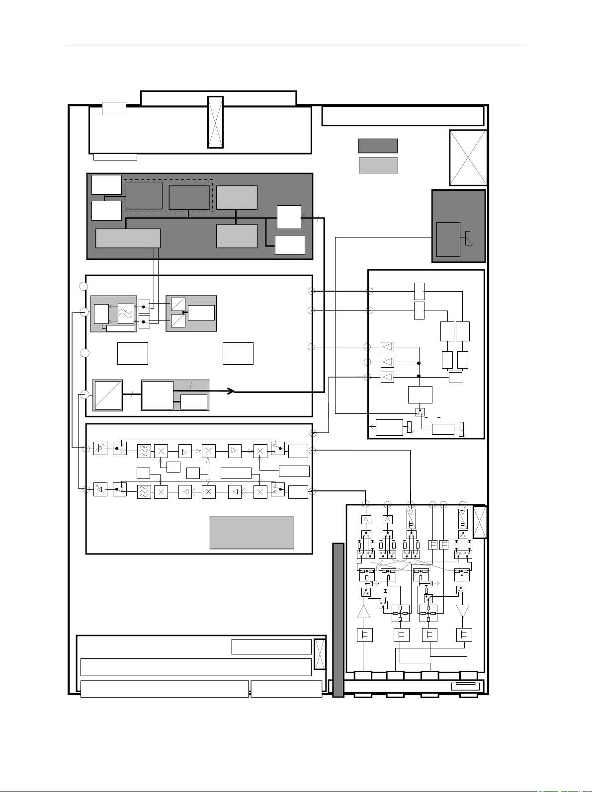
Instrument Design and Function Description R&S CMU
Block diagram
M
AINS
MICRO
PROC.
FPGA 1
S
PEECH
CODEC
CMU-B52
IQOUT MODULE
DSP
MODULE 3
FAN
POWER SUPPLY
UNIV. SIGN. UNIT 1
CMU-B21
DSP
MODULE 1
FIFO
DSP
MODULE 0
FPGA 2
INTERFACES
O
ption
S
andwich
M
odul
OCXO
REFERENCE
O
*12
2
SC.
CMU-B11/12
OCXO
FAN
R5
AUC MODULE 1 TXDSP MODULE 1
IF3TX1
IQ
MOD
I
Q
13.85MH z LO
A
D
A
D
FPGA
LINK
ADC MODULE 1 DDC MODULE 1
A
IF3RX1
12
LO3
RX
DDC
LO3
TX
IF2 487.52MHZIF3 13.85MHZ
IF2 486.515MHZIF3 10.7MHZ
D
DSP
2*12
DSP
DIGITAL BOARD
FPGA
ATDSP
RXTX BOARD 1
IF1 842.08M Hz
/1817.12 MHZ
LO1 RXLO2
IF1 843.085MHz
/1816.11 5 MHZ
TR-CORRECTION
MODULE
Attenuator
O1 TX
L
Attenuator
RFTX1
RFRX1
NETCLK2
1 to 84M Hz
2
N
ETCLK1
21 to 84MHz
110.8M3
110.8M2
110.8M1
RFRX1
REFERENCE BOARD
DI V
2/ 4
D IV
2/ 4
V CO
V CO
84 t o
16 8M H z
D DS
D DS
DIV
3
TCXO
10MHz
RFRXTXAUX1
RFRXTXAUX2
RFTX2
+5VREF
RFRX2
XTAL
110.8
MHz
RFTX1
R120
84 t o
16 8M H z
R121
FAN
FRONTMODUL
FRONT MODUL CONTROLLER
LC DISPLAY
HARDDISK
VAR/KEYBOARD
PCMCIA INTERFACE
FAN
R4IN
RF FRONTEND
RF3OUT
INTERFACES
RF2
RF1
Speaker
1100.4903.82 3.2 E-5

R&S CMU Instrument Design and Function Description
Instrument Frame
The instrument frame consists of front frame, module support, partition, cage and air duct. The module
support is screwed to the front frame. It incorporates the partition, the cage and the air duct and
provides all mechanical connectors and slots for modules. The MOTHERBOARD for electrical
connection of the modules as well as the big fan for cooling the modules are screwed to the instrument
frame.
Rear of Instrument Frame
At the rear of the R&S CMU instrument frame, the power supply with integrated power plug and switch
as well as other important electrical interfaces are fitted (see chapter 1, operating manual).
The power supply unit can be easily replaced.
A further rear panel that is screwed to the frame serves as support for further electrical interfaces and
optional extensions.
Front of Instrument Frame
The front of the instrument frame incorporates the FRONT MODULE, the most important electrical
interfaces as well as the optional FLOPPY DISK or PCMCIA INTERFACE drive.
FRONT MODULE
Electrical interfaces
Loudspeaker
The components of the FRONT MODULE that are directly arranged at
the front of the R&S CMU are the LCD and the operating keys with the
spinwheel.
The operating keys consist of a membrane and a mat inserted into the
keyboard frame of the FRONT MODULE. The operating keys are
colored differently to highlight their function and partly labeled.
This module can be conveniently replaced as a unit.
The beeper with sound outlet on the FRONT MODULE is used for
acoustic prompts and error warnings.
The electrical interfaces are mounted on an extra mounting plate. The
RF interfaces are components of the RF FRONTEND.
A loudspeaker with sound outlets at the labeling panel allows for
acoustic hints for AF signals. It is controlled via the option R&S CMUB41 AUDIO-GEN. + ANA.
1100.4903.82 3.3 E-5

Instrument Design and Function Description R&S CMU
Cooling the Instrument
Axial fan in the casing
Axial fan of power supply
Axial fan of FRONT MODULE
Axial fan of RF FRONTEND
The right side panel contains a temperature-controlled axial fan (120
mm x 120 mm x 38 mm), which sucks in cold ambient air at the right
tube of the casing and blows it through the modules via a ventilation
duct and further ventilation slots. The amount of air is controlled via the
width of the slots depending on the power dissipation of the module.
The modules are cooled by the air flow, and the heated air is then
blown out at the left side panel.
In addition, the power supply of the R&S CMU is equipped with its own
temperature-controlled axial fan (80 mm x 80 mm x 25 mm) with a
separate air circulation. The fan sucks in cold air on the left rear side of
the power supply casing and blows out the heat produced in the power
supply on the right rear side of the power supply casing.
For cooling the controller board, the FRONT MODULE is provided with
its own axial fan (40 mm x 40 mm x 10 mm), which sucks in cold
ambient air on the left side of the instrument and blows it out at the
right side panel.
The RF FRONTEND which can process powers up to 50 W is
equipped with an aluminum casing with its own air duct, cooling fins
and a temperature-controlled axial fan (40 mm x 40 mm x 20 mm),
which dissipates the heat by sucking in cold air directly on the right rear
side of the instrument and blowing in out again on the right front side of
the instrument.
The cooling concept makes sure that all components are optimally
cooled so that the complete instrument achieves a high MTBF.
1100.4903.82 3.4 E-5

R&S CMU Instrument Design and Function Description
FRONT MODULE
The FRONT MODULE consists of an aluminum case panel and a mounting plate which accommodates
the LCD, the keyboard mat with the membrane and the spinwheel.
The case panel incorporates the FRONT MODULE CONTROLLER, the fan and the hard disk.
CD
L
Operating keys
Spinwheel
FRONT MODULE
CONTROLLER
Hard disk
Fan
Connection
The color LCD provides a visible output of any information,
measurements etc. to the user.
The resolution of the LCD is 640 * 480 pixels (VGA).
The display incorporates two cold cathode tubes for the illumination.
The high voltage required for this purpose is generated in an extra
DC/AC converter mounted next to the display on the mounting plate
and connected both to the display and the controller board via a cable.
The liquid crystal display is controlled via a ribbon cable that is plugged
in on the controller board.
The operating keys consisting of a keyboard mat and a membrane
release a contact when the rubber key is pressed. Two LEDs for the
STANDBY/ON key (orange for STANDBY/green for ON) are also
accommodated on this membrane.
The rubber keys enable the user to call up all R&S CMU functions.
The key evaluation and LED control are effected via a film cable
connector on the controller board. Like the control of the two LEDs, it is
controlled in a special microprocessor on the controller board by
means of a matrix technique. This microprocessor permits to store the
status of the STANDBY/ON key when switching off using the power
switch.
The spinwheel consists of a flexible magnetic ring with individual
magnets for the lock-in positions. With each turn of the spinwheel,
electrical pulses are released from the LEDs and the optical position
detectors and sent via a ribbon cable to the microprocessor on the
FRONT MODULE CONTROLLER for evaluation.
The spinwheel serves the user as a further means of data entry and
operation.
The FRONT MODULE CONTROLLER contains all the necessary
components on a board such as processor, memory chips, I/O devices
(ISA bus), lithium battery, IEC-bus controller (IEEE), two serial
interfaces (COM1/2), a parallel interface (LPT), LCD graphics
controller, external VGA monitor graphics interface (monitor) and an
external keyboard connection (keyboard PS/2).
In addition, a floppy controller for an external floppy disk drive and an
IDE hard disk controller are integrated on the controller board.
The hard disk is screwed to the printed circuit board above the FRONT
MODULE CONTROLLER (MODEL 04) or is screwed to the rear of the
aluminum case panel (MODEL 12) and connected to the printed circuit
board via a ribbon cable.
A small axial fan in the case panel produces an air flow through the
FRONT MODULE CONTROLLER, cooling it with cold ambient air.
The FRONT MODULE is directly plugged to the MOTHERBOARD via
two 96-pin FUTURE BUS connectors (MODEL 04) and one additional
110-pin PCI Bus connector (MODEL 12).
1100.4903.82 3.5 E-5

Instrument Design and Function Description R&S CMU
POWER SUPPLY
The POWER SUPPLY of the R&S CMU consists of a two-part aluminum casing with three boards
arranged in a so-called sandwich technique (U-shape). In addition to cooling, the axial fan already
mentioned above (see cooling of instrument) is also used to support the three boards.
TANDBY/ON signal
S
Power Factor Correction
(PFC) and Standby circuit
POWERGOOD - Signal
Overtemperature
protection
AC voltage supply
Primary side
Secondary side
The control signal STANDBY/ON controlled by the FRONT MODULE
CONTROLLER (depending on the operating key STANDBY/ON on the
front of the instrument frame) activates the power supply.
The POWER SUPPLY is a primary clocked switching power supply
with Power Factor Correction (PFC) and Standby circuit (+12 V
Standby).
On the secondary side, it generates all DC voltages (+3.3 V; +5.2 V;
+6 V; +8 V; +12 V; +12 VFAN; +12 V Standby; +28 V; -12 V) for the
R&S CMU.
The secondary voltages are open-circuit-proof and short-circuit-proof
with respect to ground and each other.
When switching on and off (defined reset), the POWER SUPPLY
generates a POWERGOOD signal for control of the FRONT MODULE
CONTROLLER.
An overtemperature protective circuit is additionally installed to prevent
overheating. This status is taken to the FRONT MODULE
CONTROLLER via a status signal (OT).
A 3-pin connector with integrated 2-pin mains switch for connection
with the AC-Supply is installed on the rear panel of the POWER
SUPPLY. From there, the AC supply voltage is internally taken to the
first board via two cables.
Two fuses are also fitted there as a means of fire protection.
Note: These fuses are not accessible to the user from outside and
are only blown in the case of a serious fault of the power
supply (servicing required!).
The following circuit parts follow on the first board: EMI filter and power
rectifier. The rectified AC supply voltage is taken via a cable to the
second board of the Power Factor Correction (PFC). This circuit
converts the rectified AC supply voltage up to a constant voltage of
380 VDC. Then this voltage is taken to a step down converter which
provides a constant voltage of 280 VDC for the subsequent resonance
step down converter, which chops it with approx. 35 kHz.
An additional connecting cable is used to feed the big transformer
located on the first board. It is provided with taps for the various
secondary voltages, and the following rectifiers constitute the transition
to the DC secondary side.
The +12 V-, -12 V- and +6 V- secondary voltages are provided with
analog regulators in order to ensure a high spurious suppression.
The +3.3 V- and +5.2 V- secondary voltages have their own stepdown
converters to achieve small power dissipations.
The +28 V- voltage requires a stepup converter in order to generate
the high voltage with a high accuracy.
At the +12 VFAN, a constant current source is used for efficient
suppression of fan interference.
The secondary voltages are then filtered and subsequently taken to the
output connector.
1100.4903.82 3.6 E-5

R&S CMU Instrument Design and Function Description
Standby converter
and control unit
Connection
The third printed circuit board which serves as a connection between
the first and second board accommodates the control and monitoring
ircuit parts. Besides, it includes the standby converter, which
c
generates a +12-V standby voltage from the 380 VDC voltage of the
PFC circuit.
The POWER SUPPLY is directly connected to the MOTHERBOARD
via a 96-pin FUTURE-bus connector on the MOTHERBOARD and
screwed to the integrated rear panel of the R&S CMU with its casing.
At model SN250 (1091.1982.00) an additional 4-pin power connector is
available for connection of the option R&S CMU-B66/68 .
MOTHERBOARD
The MOTHERBOARD (1100.0908) consists of five individual printed circuit boards: MOTHERBOARD1,
MOTHERBOARD2, FRONTPANEL BOARD, REARPANEL BOARD1 and REARPANEL BOARD2.
MOTHERBOARD1
MOTHERBOARD2
FRONTPANEL BOARD
REARPANEL BOARD1
The MOTHERBOARD1 is the central motherboard and serves as
connection between most of the modules. It supplies the modules both
with voltages and control, status and bus signals in various layers
(12-layer multilayer).
The MOTHERBOARD1 accommodates various ISA bus driver devices
for the PCMCIA INTERFACE control as well as protective circuits.
These protective circuits consist of diodes and polyswitches (currentdependent, self-opening and closing fuses) and protect against
external overvoltages of the interface signals.
Nine LEDs indicate the status of the supply voltages and help with
troubleshooting.
On MOTHERBOARD1, a circuit for temperature-dependent instrument
fan control is also implemented:
The individual module temperatures are polled by the FRONT
MODULE CONTROLLER of the R&S CMU. This information is passed
on via the DIGITAL BOARD to the fan control with the aid of a control
signal. The instrument fan is controlled such that an optimum module
temperature is achieved on the one hand and as little noise as possible
is emitted by the fan on the other hand.
The MOTHERBOARD2 serves for supply and connection of the
modules located higher at the side, the REFERENCE BOARD and a
further option.
For connection with MOTHERBOARD1 two 50-pin ribbon cables are
used.
The FRONTPANEL BOARD is located at the front of the instrument
frame and accommodates the external interfaces DATA1, DATA2,
AUX3 and SPEECH. Besides, the six LEDs for the display of the active
RF inputs/outputs are located there.
For connection with MOTHERBOARD1 a 50-pin ribbon cable is used.
The REARPANEL BOARD1 is screwed to the integrated rear panel of
the R&S CMU below the POWER SUPPLY and accommodates the
external interfaces IEEE, LPT, COM1, COM2, monitor and keyboard.
For connection with MOTHERBOARD1 two 34-pin ribbon cables are
used.
1100.4903.82 3.7 E-5

Instrument Design and Function Description R&S CMU
REARPANEL BOARD2
The MOTHERBOARD (1100.2352) consists of four individual printed circuit boards: MOTHERBOARD1,
MOTHERBOARD2, FRONTPANEL BOARD and REARPANEL BOARD2.
MOTHERBOARD1
MOTHERBOARD2
FRONTPANEL BOARD
REARPANEL BOARD2
The REARPANEL BOARD2 is mounted to the right of the integrated
and unscrewable rear panel plate and accommodates the interfaces
ERVICE, AUX, AUX4 as well as further spare interfaces. For
S
connection with MOTHERBOARD1 two 34-pin ribbon cables are used.
The MOTHERBOARD1 is the central motherboard and serves as
connection between most of the modules. It supplies the modules both
with voltages and control, status and bus signals in various layers (12layer multilayer).
The MOTHERBOARD1 accommodates various ISA bus driver devices
for the PCMCIA INTERFACE control as well as protective circuits.
These protective circuits consist of diodes and polyswitches (currentdependent, self-opening and closing fuses) and protect against
external overvoltages of the interface signals.
MOTHERBOARD1 includes the external interfaces IEEE, LPT, COM1,
COM2, monitor and keyboard.
Nine LEDs indicate the status of the supply voltages and help with
troubleshooting.
On MOTHERBOARD1, a circuit for temperature-dependent instrument
fan control is also implemented:
The individual module temperatures are polled by the FRONT
MODULE CONTROLLER of the R&S CMU. This information is passed
on via the DIGITAL BOARD to the fan control with the aid of a control
signal. The instrument fan is controlled such that an optimum module
temperature is achieved on the one hand and as little noise as possible
is emitted by the fan on the other hand.
The MOTHERBOARD2 serves for supply and connection of the
modules located higher at the side, the REFERENCE BOARD and a
further option.
For connection with MOTHERBOARD1 two 50-pin ribbon cables are
used.
The FRONTPANEL BOARD is located at the front of the instrument
frame and accommodates the external interfaces DATA1, DATA2,
AUX3 and SPEECH. Besides, the six LEDs for the display of the active
RF inputs/outputs are located there.
For connection with MOTHERBOARD1 a 50-pin ribbon cable is used.
The REARPANEL BOARD2 is mounted to the right of the integrated
and unscrewable rear panel plate and accommodates the interfaces
SERVICE, AUX, AUX4 as well as further spare interfaces. For
connection with MOTHERBOARD1 two 34-pin ribbon cables are used.
1100.4903.82 3.8 E-5

R&S CMU Instrument Design and Function Description
REFERENCE BOARD
The REFERENCE BOARD provides all required clock signals (NETCLK1/2) and reference frequencies
(110.8 MHz) as well as the +5 VDC reference voltage for the R&S CMU. The REFERENCE BOARD is a
plug-in module in HVC design.
esign
D
Connection
REFERENCE
frequency generation
At the top of the module, nine MMCX connectors are attached, which
serve as inputs or outputs for various clock signals and are routed to the
respective modules or the integrated rear panel with appropriate coax
cables.
Two holes in the HVC panel at the top are used for adjusting the
+5 VDC reference voltage and the 10 MHz TCXO reference frequency.
The plug-in module REFERENCE BOARD is inserted in the R&S CMU
on the right side on MOTHERBOARD2 using a 48-pin FUTURE-bus
connector.
All frequencies provided by the R&S CMU are derived from internal highprecision 10-MHz reference elements (TCXO or optional OCXO) or from
externally applied frequencies.
A 110.8-MHz crystal oscillator is coupled in locked phase relation in a
PLL loop with the selected reference.
The reference element TCXO is used as standard on the reference
board. If the option OCXO (R&S CMU-B11 or -B12) is installed in the
R&S CMU, it is automatically used as reference element and the
standard TCXO is switched off.
It is additionally possible to switch over to external synchronization (see
Connection Control – Synch. in Chapter 4 of the R&S CMU operating
manual) and use the signal fed in at the BNC connector REF IN at the
rear of the R&S CMU as reference signal.
At the BNC connector REF OUT1 at the rear of the R&S CMU, either the
internal 10-MHz reference frequency or the signal applied at REF IN can
be buffered and tapped depending on the selected reference element.
The 110.8-MHz sinewave signal of the crystal oscillator passes a
harmonics filter, is buffered and provided at three MMXC connectors,
serving as reference frequency for the RXTX BOARD1/2 and the
DIGITAL BOARD.
At a further MMCX connector, the TTL signal RESFREQ is available with
27.7 MHz (110.8 MHz / 4) for the option R&S CMU-B41, Audio Generator
and Analyzer, as clock signal.
Netclock generation
1100.4903.82 3.9 E-5
The REFERENCE BOARD is also used for netclock generation,
providing adjustable TTL clock frequencies from 21 MHz to 84 MHz with
a very high frequency resolution of 0.1 Hz. This function is provided twice
so that two independent netclock frequencies are available at the same
time.
The signal generated by the 110.8-MHz crystal oscillator is divided by
three and applied to a DDS (Direct Digital Synthesis) circuit. The DDS
circuit is used as a fine-adjustable frequency divider and generates a
divided signal between 9 MHz and 12 MHz.
This signal is then used in a further PLL as nominal value for the phase
detector in order to tune a VCO (Voltage Controlled Oscillator) with a
tuning range of 84 MHz to 168 MHz in locked phase relation.
A fractional divider used in the feedback of the PLL provides the actual
value for the phase detector.
The output signal of the VCO is divided by two or four, buffered and
provided at the MMCX connector NETCLK 1 or NETCLK 2 and serves as
network-specific TTL clock for the DIGITAL BOARD.

Instrument Design and Function Description R&S CMU
Option OCXO REFERENCE OSC. R&S CMU-B11 or B12
This option consists of a printed circuit board with the reference element OCXO (oven-controlled crystal
oscillator), the control circuit and a potentiometer for adjusting the OCXO.
Installation
Connection
The options R&S CMU-B11 and B12 are basically of the same design. The two options only differ from
each other in the technical data of the OCXO such as aging and frequency drift.
The option OCXO REFERENCE OSC. is installed on the right side
below the instrument fan such that the potentiometer is easily
accessible from outside without the need for opening the R&S CMU
tube.
The option OCXO is directly inserted via a 10-pin connector on the
MOTHERBOARD and screwed to the module support by means of
three screws.
RF FRONTEND
Design
Cooling system
Control and supply
RF connectors
Optical indication
The printed circuit board of the RF FRONTEND is installed in a silvercoated aluminum casing which is screwed to the instrument frame. The
RF FRONTEND is fitted at the right front of the R&S CMU such that
the four RF N-type connectors which are directly connected to the
FRONTEND board are accessible on the front of the instrument frame
of the R&S CMU. This is absolutely necessary to ensure a good VSWR
(Voltage Standing Wave Ratio).
The aluminum casing in which the RF FRONTEND is installed is
equipped with cooling fins in a special cooling duct and an extra
temperature-controlled fan for heat dissipation if high RX power is fed
in.
Control and supply of the RF FRONTEND are effected from
MOTHERBOARD1 via a 34-pin ribbon cable.
For the internal RF connection to the RXTX BOARD1 (RFRX1,
RFTX1) two SMA screw connections and coaxial solid-jacket cables
are used. Thus a high-quality RF connection is ensured.
Besides, two further internal RF connections (RFRX2, RFTX2) to the
optional RXTX BOARD2 are available.
Two bidirectional monitor inputs/outputs (RFRXTXAUX1/2) at the RF
FRONTEND permit to connect further RF devices via optional cables
leading to the integrated rear panel of the R&S CMU.
As external RF interface, the RF FRONTEND is equipped with the four
N-type connectors RF1, RF2, RF3OUT, RF4IN, which permit to
perform all the RF measurements of the R&S CMU.
RF1 and RF2 are bidirectional inputs/outputs depending on the setting
and measurement application.
RF3OUT is a unidirectional output.
RF4IN is a unidirectional input.
For optical indication of the selected N-connectors and input and/or
output functions, yellow LEDs located above the N-connectors are
switched on.
1100.4903.82 3.10 E-5

R&S CMU Instrument Design and Function Description
Functions
On the transmitter side (TX), the RF FRONTEND serves the purpose
f distributing internal RF signals to the outside to the various N-
o
connectors (RF1, RF2, RF3OUT) and attenuate or amplify them
according to the selected output and level.
On the receiver side (RX), its purpose is to internally distribute external
RF signals from the different N-connectors (RF1, RF2, RF3OUT) and
attenuate or amplify them according to the selected input and the
applied level.
Since high levels and powers up to 50 W can be fed in on the receiver
side (RX), the RF FRONTEND is equipped with power attenuators and
the cooling system with the fan described above, which is controlled by
the temperature at the power attenuators.
The RF FRONTEND additionally features two broadband power
measuring diodes, which permit to measure the power applied at the
N-connectors RF1, RF2, RF4IN even in pulsed operation.
RXTX BOARD1
The RXTX BOARD1 constitutes the central RF board which contains all circuit parts for conversion from
RF to IF both for the transmitter (TX) and receiver (RX).
Design
Cooling system
Control and supply
Complete function
Transmitter functions
The RXTX BOARD1 is designed as plug-in module with a silver-coated
two-shell aluminum casing fixed with several screws.
This casing is equipped with cooling fins at the front and rear which are
provided with a cover sheet each so that two special cooling ducts are
produced. These cooling ducts are evenly cooled by the air flow of the
instrument fan irrespective of neighboring modules.
This efficient cooling is required since a very high degree of integration
and a large portion of fast RF components are implemented on this
board.
Control and voltage supply of the RXTX BOARD1 are effected via a
96-pin FUTURE-bus connector from MOTHERBOARD1.
For conversion from RF to IF, the transmitter side (TX) is implemented
on one side of the multilayer PC board and the receiver side (RX) on
the other side on the RXTX BOARD1. This strict separation of the
functions permits to achieve high decouplings as they can usually only
be achieved with two separate modules.
On the transmitter side (TX), an IF signal with 13.85 MHz is applied at
the MMCX connector IF3TX1 (top of module) of the RXTX BOARD1,
which is provided by the DIGITAL BOARD.
On the RXTX BOARD1, this signal is taken via various amplifier
stages, attenuator pads and filters and finally set to the desired RF
frequency by means of triple signal conversion (IF3, IF2, IF1). This is
necessary to obtain a high image-frequency rejection.
At the TX output, a switchable attenuator with fine stepping and large
attenuation range is used to set the RF signal amplitude according to
the level selected.
The RF signal is finally taken to the RF FRONTEND at the SMA
connector RFTX1 (bottom of module).
1100.4903.82 3.11 E-5

Instrument Design and Function Description R&S CMU
The transmitter side is provided with an extra LO1TX (Local Oscillator)
ith large tuning range and very fine frequency resolution used for
w
setting the desired transmitter frequency, an LO2 fixed-frequency
oscillator shared with the receiver side and an extra LO3TX with small
tuning range. All LOs are synchronized by the MMCX connector
110.8MHz at the bottom of the module with the reference frequency
from the REFERENCE BOARD.
Besides, an MMCX connector at the top of the RXTX BOARD1 is
designed as input with the second transmitter IF (RESIF2TX) which is
activated via software switches.
Receiver functions
Correction processor
Extension
On the receiver side (RX), the RF signal is fed in at the SMA connector
RFRX1 (bottom of module) of the RXTX BOARD1 which is provided by
the RF FRONTEND.
On the RXTX BOARD1, this signal is taken via a switchable attenuator
with fine stepping and large attenuation range in order to match the
level according to the level applied.
Subsequently, this signal is converted to an IF frequency of 10.7 MHz
by means of triple signal conversion (IF1, IF2, IF3) and several filter
and amplifier stages and provided at the MMCX connector IF3RX1 (top
of module) for the DIGITAL BOARD.
This procedure is necessary to achieve a high image-frequency
rejection and a high dynamic range with a simultaneously high
intermodulation suppression.
For the receiver side, an extra LO1RX (local oscillator) is provided with
a large tuning range and a very fine frequency resolution used for
setting the receive frequency, an LO2 fixed-frequency oscillator shared
with the transmitter and an extra LO3RX with a very small tuning
range.
All LOs are synchronized by the MMCX connector 110.8 MHz at the
bottom of the module with the reference frequency from the
REFERENCE BOARD.
A further MMCX connector RESIF3RX (top of module) provides a
buffered RX IF signal of 10.7 MHz which is taken to the rear of the
R&S CMU via a coax cable. This signal output can be activated via a
software switch.
Besides, an MMCX connector at the top of the RXTX BOARD1 is
designed as output with the second receiver IF (RESIF2RX) which can
be activated via software switches.
The RXTX BOARD1 contains an extra correction processor with large
flash PROM.
It controls all the static and dynamic settings on the RXTX BOARD1
and, as a special feature, also the attenuator pads and amplifiers of the
RX and TX attenuator on the RF FRONTEND.
Besides, the correction processor permits to read out the individual
module error data from the EEPROMS of the respective modules in a
so-called correction procedure (automatic module data adjustment)
and calculate the deviations for all possible signal paths. These
deviations are stored as correction values in the flash PROM. The
correction processor then sets the desired level settings, corrected by
the correction values, in the flash PROM so that frequency, linearity
and temperature responses of the modules are compensated for.
This ensures the excellent level accuracy of the R&S CMU which is
essential for most measurements.
The R&S CMU 200 can be extended by a RXTX BOARD2 and thus
provide a second complete transmit and receive channel.
1100.4903.82 3.12 E-5

R&S CMU Instrument Design and Function Description
DIGITAL BOARD
The DIGITAL BOARD constitutes the central control and measurement board which contains all circuit
parts for conversion and further processing of the analog IF (receiver side) into digital I/Q values.
On the transmitter side, analog as well as digital I/Q values are modulated upon the carrier and provided
as analog IF.
Design
Cooling system
Control and supply
Function
ADC MODULE1
DDC MODULE1
The DIGITAL BOARD is designed as HVC 200 plug-in module. The
HVC 200 cabinet is equipped with a screwed-on cover both at the front
and rear to ensure optimum electrical shielding of the module.
The casing is provided with ventilation holes on the right and left in
order to produce a large cooling flow through the module by means of
the instrument fan.
This efficient cooling is necessary, since a great number of highly
integrated fast digital devices is used on the module and up to eight
sandwich modules can additionally be fitted so that the board is
densely packed.
The control, bus lines and voltage supply of the DIGITAL BOARD are
effected via four 96-pin and one 48-pin FUTURE-bus connectors from
MOTHERBOARD1.
As standard, the four sandwich boards ADC Module1, DDC Module1,
TXDSP Module1 and AUC Module1 are fitted.
On the DIGITAL BOARD, all necessary clocks are generated and
provided from the netclocks 1 and 2 in a clock conditioning and
distribution circuit. These clocks are required for sampling, filtering and
down converting the digital IF internally and for the UNIVERSAL
SIGNALLING UNIT MODULE.
Besides, two programmable logic devices (FPGA) are used on the
DIGITAL BOARD, which provide address decoding, interrupt control
and host interfaces between ISA bus and internal circuit parts
(DDC/TXDSP) as well as the control of the RF FRONTEND (via FEI
Bus), the REFERENCE BOARD and AUDIO BOARD (via buffered ISA
bus) and the RXTX BOARD1 (via serial bus). Further serial interfaces
lead from the programmable logic devices to the UNIVERSAL
SIGNALLING UNIT1 and vice versa.
An AD converter on the DIGITAL BOARD is used for polling the
diagnostic voltages of the R&S CMU modules, which can indicate
module states and errors.
The sandwich ADC MODULE1 is connected to the DIGITAL BOARD
via a multipoint connector. In addition, it is screwed to a solid ground
block to obtain a good ground connection.
The ADC MODULE1 receives the analog IF (10.7 MHz) from the RXTX
BOARD1 directly via a MMCX connector (IF3RX1) and converts it into
a 12-bit data stream by means of a fast AD converter.
The sandwich DDC MODULE1 is directly plugged onto the DIGITAL
BOARD via three multipoint connectors and processes the digital data
stream of the receiver. In a special ASIC chip, the I/Q shaping, the
matching of the data rate and the respective filtering (bandwidth
shaping) of the digital data stream are produced. Then follows a DSP
(RX DSP) with further evaluation of the digital I/Q data for
measurement purposes. Besides, the digital I/Q data are passed on via
the MOTHERBOARD1 to the LINKHANDLER MODULE for evaluation.
2
C-
1100.4903.82 3.13 E-5

Instrument Design and Function Description R&S CMU
TXDSP MODULE1
AUC MODULE1
Extension
The sandwich TXDSP MODULE1 is directly plugged onto the DIGITAL
BOARD via two multipoint connectors. It contains the DSP on the
ransmitter side (TXDSP), which generates I/Q data according to the
t
application and provides them to the AUC MODULE1 via two 12-bit
D/A converters and several selection switches located on the DIGITAL
BOARD.
The sandwich AUC MODULE1 is directly plugged onto the DIGITAL
BOARD via a multipoint connector and serves the purpose of filtering
the analog I/Q data from the TXDSP MODULE1 or the LINKHANDLER
MODULE depending on the position of the selection switches on the
DIGITAL BOARD according to the application (bandwidth shaping) and
converting it to the transmit IF (13.85 MHz) by means of an I/Q
modulator. Subsequently, the transmit IF is routed via the MMCX
connector (IF3TX1) on the DIGITAL BOARD to the RXTX BOARD1.
The DIGITAL BOARD can be extended by a further complete receive
and transmit channel consisting of ADC MODULE2, DDC MODULE2,
TXDSP MODULE2 and AUC MODULE2.
Option UNIVERSAL SIGNALLING UNIT R&S CMU-B21 Var02
The UNIV. SIGN. UNIT MODULE is the control and measurement module which contains all circuit
parts for signaling and measuring network-specific parameters.
To this end, the digital I/Q data from the DIGITAL BOARD are used on the receiver side (RX) in order to
calculate test parameters.
On the transmitter side, analog network-specific I/Q data are generated and provided to the AUC
MODULE1 on the DIGITAL BOARD.
Design
Cooling system
Control and supply
Function
The UNIV. SIGN. UNIT MODULE is designed as plug-in module with
two aluminum shell covers. It is equipped with a screwed-on aluminum
cover both at the front and rear to allow for optimal electrical shielding
of the module.
The casing is provided with ventilation holes on the right and left in
order to produce a large cooling flow through the module by means of
the instrument fan.
This efficient cooling is necessary, since a great number of highly
integrated fast digital devices is used on the module and up to seven
sandwich modules can additionally be fitted so that the module is
densely packed.
The control, bus lines and voltage supply of the UNIV. SIGN. UNIT
MODULE are connected via two 96-pin VG multipoint connectors from
MOTHERBOARD1. Further interfaces for testing and debugging are
provided on the top of the module.
As standard, the UNIV. SIGN. UNIT MODULE contains the three
sandwich boards DSP MODULE0, DSP MODULE1 and IQOUT
MODULE.
Besides, if a very high computing power is required, two further DSP
MODULES (DSP MODULE2, DSP MODULE3) and the SHARED
MEMORY can be fitted.
Furthermore, a slot for the Option R&S CMU-B52 SPEECH CODEC is
provided. This option includes DSP MODULE3.
1100.4903.82 3.14 E-5

R&S CMU Instrument Design and Function Description
A microprocessor with peripheral equipment and two FPGA’s on the
UNIV. SIGN. UNIT control all the processes on the module.
n RS232 interface is available for debugging, data input and output.
A
Besides, an ISA bus interface is installed for control and data
communication with the FRONT MODULE CONTROLLER.
DSP MODULE
Option BLUETOOTH
MODULE
R&S CMU-B53 Var02
The two sandwich DSP MODULES (DSP MODULE0 and DSP
MODULE1) are directly inserted on the UNIV. SIGN. UNIT via four
multipoint connectors. Via a FIFO device, they receive the digital I/Q
data from the DIGITAL BOARD for evaluation. The signal can then be
demodulated by the DSP MODULES and the demodulated data can be
passed on the protocol engine running on the MC or a DSP MODULE.
The DSP MODULES can also perform some measurements and the
results are passed on via the ISA bus interface to the FRONT
MODULE CONTROLLER.
Likewise, the DSPs cause further actions on the transmitter side (TX),
e.g. change transmit frequency-settings via the FPGA 'XILINX2' and
output analog I/Q data via the IQOUT MODULE.
The option BLUETOOTH MODULE R&S CMU-B53 Var02 is directly
inserted on the UNIV. SIGN. UNIT. It performs BLUETOOTH
functionality.
Attention: This option includes the functionality of option SPEECH
CODEC R&S CMU-B52 Var02. Therefore it is not necessary and
possible to fit additionally the option SPEECH CODEC R&S CMU-B52
Var02.
IQOUT MODULE
Option SPEECH CODEC
R&S CMU-B52 Var02
The sandwich IQOUT MODULE is directly inserted on the UNIV. SIGN.
UNIT via three multipoint connectors and installed in an extra shielding
chamber, since it performs the digital-to-analog conversion of the I/Q
data.
The Option SPEECH CODEC R&S CMU-B52 Var 02 (including DSP
MODULE3) is also designed as sandwich module and is directly
plugged onto the UNIV. SIGN. UNIT via three multipoint connectors.
This option permits to read in and output analog speech signals
(handsetin/out lines) via A/D and D/A converters.
1100.4903.82 3.15 E-5

Instrument Design and Function Description R&S CMU
Option UNIVERSAL SIGNALING UNIT R&S CMU-B21 Var 14/54
The UNIV. SIGN. UNIT MODULE is the control and measurement module which contains all circuit
parts for signaling and measuring network-specific parameters.
To this end, the digital I/Q data from the DIGITAL BOARD are used on the receiver side (RX) in order to
calculate test parameters.
On the transmitter side, analog network-specific I/Q data are generated and provided to the AUC
MODULE1 on the DIGITAL BOARD.
Design
Cooling system
Control and supply
Function
Option DSP MODULE 3
R&S CMU-B55 Var14
Option SIGNALING MODULE
R&S CMU-B54 Var14
The UNIV. SIGN. UNIT MODULE is designed as plug-in module with
two aluminum shell covers. It is equipped with a screwed-on aluminum
cover both at the front and rear to allow for optimal electrical shielding
of the module.
The casing is provided with ventilation holes on the right and left in
order to produce a large cooling flow through the module by means of
the instrument fan.
This efficient cooling is necessary, since a great number of highly
integrated fast digital devices is used on the module and up to six
sandwich modules can additionally be fitted so that the module is
densely packed.
The control, bus lines and voltage supply of the UNIV. SIGN. UNIT
MODULE are connected via two 96-pin VG multipoint and one 48-pin
VG multipoint connectors from MOTHERBOARD1. Further interfaces
for testing and debugging are provided on the top of the module.
As standard, the UNIV. SIGN. UNIT MODULE VAR14 contains four
DSP’s (DSP 0 and DSP 1, CPDSP 1 and CPDSP 2) and is provided for
six sandwich modules.
As model Var54 the UNIV. SIGN. UNIT MODULE VAR54 contains
UNIV. SIGN. UNIT MODULE VAR14 and the two sandwich boards
MC68K MODULE and DSP2 MODULE.
Besides, if a very high computing power is required, one further DSP
MODULE (DSP MODULE3, Option R&S CMU-B55Var14) can be
fitted.
Furthermore, a slot for the Option R&S CMU-B52 SPEECH CODEC
Var 14 is provided.
Furthermore, a slot for the Option R&S CMU-B56 Var14/54 POWER
PC MODULE is provided.
One FPGA on the UNIV. SIGN. UNIT control all the processes on the
module.
An RS232 interface is available for debugging.
Besides, an ISA bus interface is installed for control and data
communication with the FRONT MODULE CONTROLLER.
The sandwich DSP MODULE 3 R&S CMU-B55 Var14
is directly inserted on the UNIV. SIGN. UNIT. It performs more than
two uplinks at GSM.
The option SIGNALING MODULE R&S CMU-B54 Var14 contains the
two sandwich boards DSP MODULE 2 and MC68K MODULE. These
modules are directly inserted on the UNIV. SIGN. UNIT. It performs
GSM, TDMA, AMPS functionality.
Option R&S CMU-B54 Var14 is included in UNIV. SIGN. UNIT
MODULE R&S CMU-B21 VAR54.
1100.4903.82 3.16 E-5

R&S CMU Instrument Design and Function Description
Option POWER PC
R&S CMU-B56 Var14
Option HIGH SPEED POWER
PC
R&S CMU-B56 Var54
Option BLUETOOTH
MODULE
R&S CMU-B53 Var14
Option SPEECH CODEC
R&S CMU-B52 Var14
The option POWER PC R&S CMU-B56 Var14 is directly inserted on
the UNIV. SIGN. UNIT. It performs WCDMA signaling function.
his option can be fitted only without the option R&S CMU-B56Var54.
T
The option HIGH SPEED POWER PC R&S CMU-B56 Var54 is directly
inserted on the UNIV. SIGN. UNIT. It performs high performance
WCDMA signaling function at data end to end tests.
This option can be fitted only without the option R&S CMU-B56Var14.
The option BLUETOOTH MODULE R&S CMU-B53 Var14 is directly
inserted on the UNIV. SIGN. UNIT. It performs BLUETOOTH
functionality.
Attention: For Bluetooth Speech Tests the Option SPEECH CODEC
R&S CMU-B52 Var14 is additionaly necessary.
The Option SPEECH CODEC R&S CMU-B52 Var14 ( Speech Codec
and DSP at one Sandwich module) is also designed as sandwich
module and is directly plugged onto the UNIV. SIGN. UNIT. This option
permits to read in and output analog speech signals (handsetin/out
lines) via A/D and D/A converters.
1100.4903.82 3.17 E-5

Instrument Design and Function Description R&S CMU
generation circuit, an analog input section and an analog output section
Option AUDIO-GEN. + ANA. R&S CMU-B41
The Option AUDIO-GEN. + ANA. constitutes the central AF-board which contains all circuit parts for
generation of AF output and analysis of AF input signals. The Option AUDIO-GEN. + ANA. is a plug-in
module in HVC design.
esign
D
Connection
Function
Analog Input Section
Analog Output Section
At the top of the module, eight MMCX connectors are attached, which
serve as inputs or outputs for AF and clock signals and are routed to
the respective modules or the integrated front panel with appropriate
coax cables. There is also a coax cable to the loudspeaker on the front
panel.
The plug-in module AUDIO-GEN. + ANA. is inserted in the R&S CMU
on the right side on MOTHERBOARD2 using a 96-pin FUTURE-bus
connector.
The Option AUDIO-GEN. + ANA. contains one DSP MODULE, a clock
Further there is a power amplifier for the loudspeaker on this board
The DSP MODULE is a sandwich module, which controls the signal
path, level and frequency of the AF output generator and also the
signal path, attenuation and analysis of the AF input analyzer.
The DSP MODULE is connected via an ISA-Bus Interface to the
FRONTMODULE CONTROLLER of the R&S CMU.
The clock generation circuit gets from the REFERENCE BOARD a
27.7MHz signal over a coax cable and a MMCX connector. This signal
feeds the DSP MODULE and is converted in a PLL circuit to 24.576
MHz.
Over a divider by 2 to. This clock signal divided by 2 (12.288MHz) is
used for the A/D and D/A Converter IC and the serial links.
Over the BNC connectors AFIN and AUX1 at the front of the R&S
CMU and the coax cables the AF signal comes to the analog input
section, which provides two independent input channels.
These two Input channels could be used as one balanced or two
unbalanced channels. Over an input attenuator and an various gain
amplifier per channel the AF signal comes to the A/D Converter, which
sends over a serial link connection the digital values to the DSP
MODULE.
For the AF-Generator the DSP MODULE sends the digital values over
a serial link connection to the D/A Converter of the analog output
section.
The analog output section provides two independent output channels,
which could be used as one balanced or two unbalanced channels.
Over a various gain amplifier and a switchable output attenuator the
AF signal comes to the MMCX connectors, which are connected via
coax cables to the BNC connectors AFOUT and AUX2 at the front of
the R&S CMU.
1100.4903.82 3.18 E-5

R&S CMU Instrument Design and Function Description
Option WCDMA L1COPRO R&S CMU-B66/68/76/78
The WCDMA L1COPRO MODULE is the control and measurement module which contains all circuit
parts for signaling and measuring network-specific parameters.
To this end, the analog IF signal from the RXTX BOARD are used on the receiver side (RX) in order to
calculate test parameters (only with R&S CMU-B68/78).
n the transmitter side, analog network-specific IF signal data are generated and provided to the RXTX
O
MODULE.
Design
Cooling system
Control and supply
Function
WTX MODULE
TX-FEC MODULE
WDDC MODULE
(only with Option
R&S CMU-B68/78)
RX-FEC MODULE
(only with Option
R&S CMU-B68/78)
The WCDMA L1COPRO MODULE is designed as plug-in module with
two aluminum shell covers. It is equipped with a screwed-on aluminum
cover both at the front and rear to allow for optimal electrical shielding
of the module.
The casing is provided with ventilation holes on the right and left and
additional cooling fins at the rear which are provided with a cover sheet
so that one special cooling duct are produced in order to produce a
large cooling flow through the module and the duct by means of the
instrument fan.
This efficient cooling is necessary, since a great number of highly
integrated fast digital devices is used on the module and up to four
sandwich modules can additionally be fitted so that the module is
densely packed.
The control, bus lines and voltage supply of the WCDMA L1COPRO
MODULE are connected via two 96-pin VG and one 48-pin VG
multipoint connectors from MOTHERBOARD1. Further interfaces for
IF IN and IF OUT are provided on the top of the module.
As standard (R&S CMU-B66/76), the WCDMA L1COPRO MODULE
contains the two sandwich boards WTX MODULE and TX-FEC
MODULE.
As Option R&S CMU-B68/78, the WCDMA L1COPRO MODULE
contains the two two sandwich boards WTX MODULE, TX-FEC
MODULE and additional the two sandwich boards WDDC MODULE
and RX-FEC MODULE.
Three FPGA’s on the WCDMA L1COPRO MODULE control all the
processes on the module. Two DSP’s, one for TX and one for RX,
generate and analyse the signals TX-FEC MODULE and RX-FEC
MODULE. See Figure 3-2 for a simplified block diagram.
Besides, an ISA bus interface is installed for control and data
communication with the FRONT MODULE CONTROLLER.
The sandwich WTX MODULE is directly inserted on the WCDMA
L1COPRO MODULE. It performs the digital-to-analog conversion of
the TX IF output signal.
The sandwich TX-FEC MODULE is directly inserted on the WCDMA
L1COPRO MODULE. It performs the forward error correction of the
digital TX data.
The sandwich WDDC MODULE is directly inserted on the WCDMA
L1COPRO MODULE. It performs the analog-to-digital conversion of
the RX IF input signal.
The sandwich RX-FEC MODULE is directly inserted on the WCDMA
L1COPRO MODULE. It performs the forward error correction of the
digital RX data.
1100.4903.82 3.19 E-5

Instrument Design and Function Description R&S CMU
W-Coprocessor - Board
I
F
W-DDC-Modul
W
- DDC-
CPLD
3
2
W-RX-Transf er- Bus
3
2
W-TX-Transf er- Bus
I
I
2C Bus
SP/JTAG
F
D-RA M_1
F
D-RA M_2
A
DD-RA M_ 1
A
DD-RA M_ 2
I
Q
S
D
ync-
emod-
FPGA
FPGA
1
2
D
emod-
DPR_1
FPGA Download
FPGA Download
I2C BusI2C Bus
W
-RX-FEC-Module
FPGA Download
Linkport (4 Bit)
1 RX-FEC-RX-DSP
*
(4 Bit)
(4 Bit)
1 RX/TX-FEC-Linkport
1 RX/TX-FEC-Linkport
*
RX/TX-Link-Bus (2 Linkports)
C
CPLD
B
oot
Link
W-RX-
W
-RX - DSPR
AM
DSP
W
-RX-DSP- Bus
R
X-DSPBuffer
S-
ISP/ JTAG
R
Logging-
RAM
RX/TX-
B
US-DPR
X-
2XLink port
RX-SPORT_1/2
FPGA Download
Connector
B
US/ I NTF
PGA
:best ückungsv ari ant ,
*
Default wiei n Zeichnung
U
SU-SER-Bus
3
Protocol l Board 1
T
T
X-COM-
X-DAT-
D
PR
W-CDMA- T X-
M
odul
I2C Bus
B
oot Link
D
PR
FPGA Download
C
P
ower
supply
lk
FPGA Download
Linkport (4 Bit)
1 TX-FEC-TX-DSP
W-TX-FEC-Module
I
F
Figure 3-1: WCDMA L1COPRO block diagram
TX-DSP-
W-TX-
D
RX-ISA-
W-TX-DSP-
RAM
L
TXoggingR
AM
T
X-SPORT_1/ 2
Buffer
W-TX- DSP- Bus
SP
Boot
L
ink
FPGA Download
ISP/ JTAG
B
oot Link
DPR
ISA-IF-
CPLD
TX-I SA-
DPR
I2C Bus
I2C
P
rot ocol l Board 2
AT
TX-Module-SPORT_1
2
XLink por t
Mod u l es
F
PGA
DSP
D
PR
Link por t
S
eri al
ISP/ J TAG
Boot Li nk
F
PGA
D
ownload
I2C
1100.4903.82 3.20 E-5

R&S CMU Instrument Design and Function Description
Option CDMA (IS95) Signaling Unit R&S CMU-B81
The CDMA (IS95) Signalling Unit is a module of the R&S CMU200 providing signalling and measuring
support for the CDMA IS-95 cellular phone network.
With the use of analog and digital hardware and firmware, this module uses the down converter and a
signal generator in the R&S CMU200 to establish a link with a CDMA mobile station.
Design
Cooling system
The CDMA (IS95) Signalling Unit is a plug-in module with a complete
aluminum shell providing optimal electrical shielding of the module.
Ventilation holes on the right and left of the shell produces a large cooling
flow through the module by means of the instrument fan.
Control and supply
Function
CMU Plat form
RF
The MOTHERBOARD 1 provides bus lines, the voltage supply, and controls
the CDMA (IS95) Signalling Unit via two 96-pin connectors and one 48-pin
connector. Further interfaces for testing and debugging are provided on the
top of the module.
The CDMA (IS95) Signalling Unit contains the hardware for signal
demodulation and signal generation of a CDMA system. See Figure 3-2 for
a simplified block diagram.
A micro processor with peripheral equipment and three programmable logic
devices (Xilinx 1, 2, and 3) on the board control all the processes on the
module.
An RS232 interface is available for debugging and data input and output.
An AT-bus interface is used for control and data communication with the
front module computer.
FrontEnd
Board
CMU ControllerFront / Rear Panel
RxTx
Board
Digital
Up / Down
Conversion
Dig. I & Q
Measurement
DSP
System Clock
Generation
External
Interfaces
Expansion Interfaces
LinkHandler
Processor / Memory
CDMA LinkHandler
CMU
Internal
Interfaces
Internal
Interfaces
Vocoder
Interface
CDMASupport
CDMA
Demodulation
CDMA Signal
Generation
AWGN
Generator
Output Signal
Conditioning
Synchronization
Clock / Trigger
System
I
Q
Triggers
NetClock
Figure 3-2: CDMA (IS95) Signalling Unit block diagram
1100.4903.82 3.21 E-5

Instrument Design and Function Description R&S CMU
Option CDMA2000 Signaling Unit R&S-B83 Var12
The CDMA2000 Signalling Unit is a module of the R&S CMU200 providing signalling and measuring
support for the CDMA2000 cellular phone network.
With the use of analog and digital hardware and firmware, this module uses the down converter and a
signal generator in the R&S CMU200 to establish a link with a CDMA mobile station.
Design
Cooling system
The CDMA2000 Signalling Unit is a plug-in module with a complete
aluminum shell providing optimal electrical shielding of the module.
Ventilation holes on the right and left of the shell produces a large cooling
flow through the module by means of the instrument fan.
Control and supply
Function
1xEV-DO Module
R&S CMU-B88
Access Module
R&S CMU-B82
Speech Codec Module
R&S CMU-B85 VAR02
Message Monitor
R&S CMU-B87
The MOTHERBOARD 1 provides bus lines, the voltage supply, and controls
the CDMA2000 Signalling Unit via two 96-pin connectors and one 48-pin
connector. Further interfaces for testing and debugging are provided on the
top of the module.
The CDMA2000 Signalling Unit contains the hardware for signal
demodulation and signal generation of a CDMA2000 system. See Figure
3-2 for a simplified block diagram.
A POWER PC with peripheral equipment and one FPGA with peripheral
ASIC on the board control all the processes on the module
An Ethernet interface is available for data input and output (Option R&S
CMU-B87).
An RS232 interface is available for debugging.
An AT-bus interface is used for control and data communication with the
front module computer.
The Option 1xEV-DO Module R&S CMU-B88 is designed as sandwich
module and is directly plugged onto the CDMA2000 SIGN. UNIT. This
option permits to generate 1xEV-DO TX Non Signaling signals.
The Option Access Module R&S CMU-B82 is designed as sandwich module
and is directly plugged onto the CDMA2000 SIGN. UNIT. An additional
cable to the rearpanel of the R&S CMU is included. This option permits
access to the special Access Interface.
This option can be fitted only without the option R&S CMU-B85.
The Option SPEECH CODEC R&S CMU-B85 is designed as sandwich
module and is directly plugged onto the CDMA2000 SIGN. UNIT. This
option permits to read in and output analog speech signals (handsetin/out
lines) via A/D and D/A converters.
This option can be fitted only without the option R&S CMU-B82.
This Option Message Monitor R&S CMU-B87 is designed as a cable to
connect the CDMA2000 SIGN. UNIT with the rearpanel of the R&S CMU
1100.4903.82 3.22 E-5
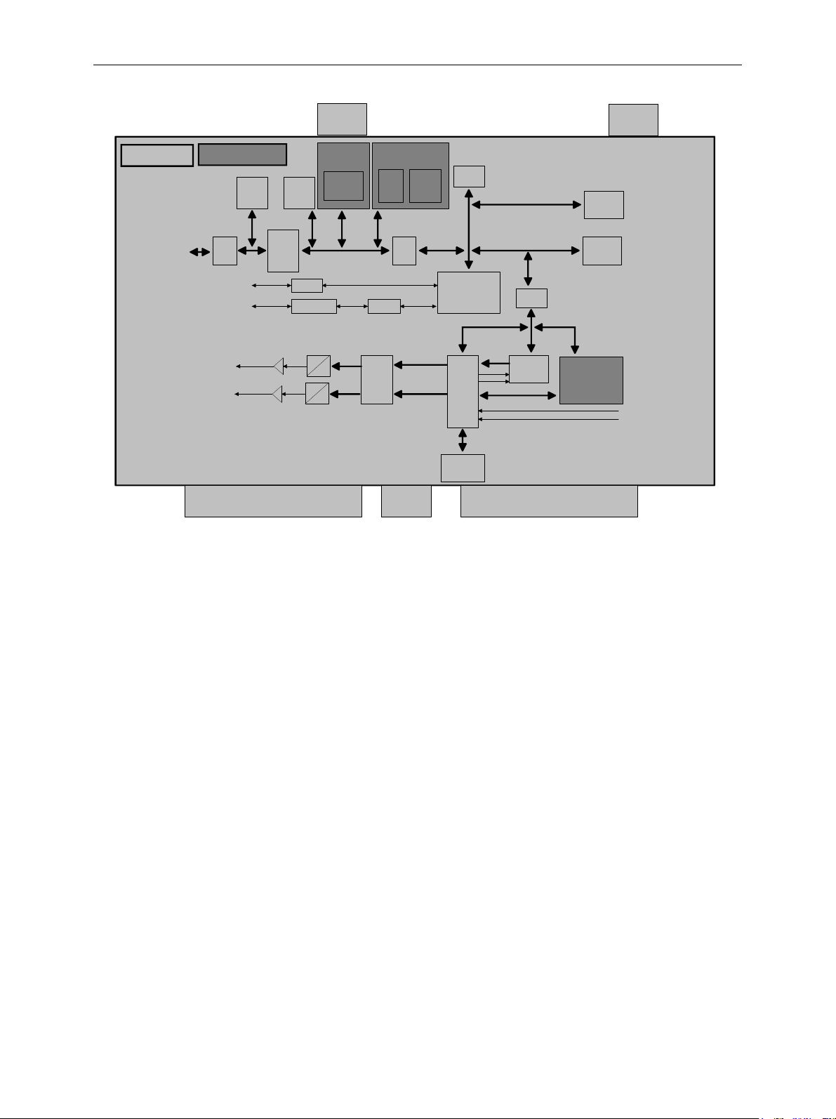
R&S CMU Instrument Design and Function Description
Grundboard
I
SA-Bus
Sandwich Module
LVT
245
S
D0..7
2 x RS232
E
thernet
AUC
on
Digitalboard
I
Q
ISAControl/
Status
Register
CMD
D0..7
X61
D
PR
2K x 8
PPCControl/
Status
Register
R
S232
B
uffer
E
thernet
Transformer
A
Digital I/Q
CMU-B82
CMU-B82
Access Module
I/O Interface
D0..7
(A16..31)
A
D
D
CMU-B85
Speech Codec Module
DSP
Audio Codec
5
6311
1 x Data
2 x Address
3
x
L
VT
245
L
TX971
Level
Shifter
3V-->5V
I0..15
Q0..15
X62
0..7
P
ower P C (PPC )
MPC860P
80 MH z
XILINX
XCV400
B
SRAM
512K x 16
P
Config-
Register
GA560
0..31
PC-
0
..15
P
DATA 0..31
(PADDR 0..31)
CSM Out
I
Q
LVT
1
6245
CSM
5000
HDR_SPARE
0..39
D
ATA 0..31
(A16..31)
0..31
0
..11
0..11
X63
0
..31
0..15
CMU-B88
1
xEV-DO Module
Non Signaling
0..31
S
DRAM
4M x 32
A
MD
F
LASH
4M x 16
Digital I
Dig ital Q
X600
Et her net
Digital I/Q
from
Digitalboard
Figure 3-3: CDMA2000 Var12 Signalling Unit block diagram
Option CDMA2000 Signaling Unit R&S CMU-B83 Var22
The CDMA2000 Signalling Unit is a module of the R&S CMU200 providing signalling and measuring
support for the CDMA2000 cellular phone network.
With the use of analog and digital hardware and firmware, this module uses the down converter and a
signal generator in the R&S CMU200 to establish a link with a CDMA mobile station.
Design
Cooling system
Control and supply
Function
The CDMA2000 Signalling Unit is a plug-in module with a complete
aluminum shell providing optimal electrical shielding of the module.
Ventilation holes on the right and left of the shell produces a large cooling
flow through the module by means of the instrument fan.
The MOTHERBOARD 1 provides bus lines, the voltage supply, and controls
the CDMA2000 Signalling Unit via two 96-pin connectors and one 48-pin
connector. Further interfaces for testing and debugging are provided on the
top of the module.
The CDMA2000 Signalling Unit contains the hardware for signal
demodulation and signal generation of a CDMA2000 system. See Figure
3-2 for a simplified block diagram.
A high performance POWER PC Module with peripheral equipment and one
FPGA with peripheral ASIC on the board control all the processes on the
module
1100.4903.82 3.23 E-5

Instrument Design and Function Description R&S CMU
An Ethernet interface is available for data input and output (Option R&S
CMU-B87).
An RS232 interface is available for debugging.
An AT-bus interface is used for control and data communication with the
front module computer.
1xEV-DO Module
R&S CMU-B89
The Option 1xEV-DO Module R&S CMU-B89 is designed as sandwich
module and is directly plugged onto the CDMA2000 SIGN. UNIT Var22.
This option permits to generate 1xEV-DO Signaling signals.
Speech Codec Module
R&S CMU-B85 Var22
Message Monitor
R&S CMU-B87
AFGENMON
Handset In
Handset Out
Netclk CLK-
Dig. I/Q-IN
TX-I
TX-Q
MUX
MUX
A
A
The Option SPEECH CODEC R&S CMU-B85 Var22 is designed as
sandwich module and is directly plugged onto the CDMA2000 SIGN. UNIT.
This option permits to read in and output analog speech signals
(handsetin/out lines) via A/D and D/A converters.
This Option Message Monitor R&S CMU-B87 is designed as a cable to
connect the CDMA2000 SIGN. UNIT with the rearpanel of the R&S CMU
Ether net
Ethernet
Power-PC-Module
CMU-B85 Var22
Speech Codec Module
Codec
Distrib.
D
3V
5V
D
3V
5V
FPGA
FIR
FIR
XC2V2000
Dual-Port-RAM, Registers,..
CMU-B89
1xEVDO-Module
Signaling
PPC-PCI-Bus
(32 Bit/33MHz)
Local-Bus
(32 Bit)
CSM 5000
FLASH
32M x 16
DDR-SDRAM
32Mx64
Power PC
MPC8540
700 MHz
Ethernet
RS232
Test
+5V
DC
DC
+1.5V
+1.2V
+1.5V
+1.8V
SUP_MODUL
SUP_MODUL
SUP_FPGA
SUP_DSP
AWGN-
SSRAM
512Kx36
Control-/
Sync-Bus
Test/
LED/
Debug
ISA-Interface
(Buffer + Register)
ISA-Bus
3GPP2-Linkhandler
LH_3GPP2.DRW
Figure 3-4: CDMA2000 Var22 Signalling Unit block diagram
1100.4903.82 3.24 E-5

R&S CMU MODULE Replacement
MODULE Replacement
Caution!
Disconnect the instrument from the mains before opening the casing. Please
note the safety instructions at the beginning of this manual.
When mounting the tube take care not to damage or pull off cables.
Replacing the FRONT MODULE
(see chapter 5, spare part list, Current No. 10X to 103, and explosion drawing 1100.0008.01 D sheet 2)
For replacement proceed as follows:
Opening the instrument and removing the FRONT MODULE
Switch off the instrument, pull the mains plug and unscrew the rear-panel feet.
Place the instrument onto the front carrying handles, push the tube upwards and take off.
Unscrew the four screws of the front handles at the instrument frame on both sides and take off the
front handles.
Unscrew a countersunk screw (if present) at the front on the labeling panel next to the spinwheel and
pull off the labeling panel towards the front.
Unscrew two countersunk screws in the front frame at the top and at the bottom as well as two
countersunk screws at the front above the AUX1/2 BNC connectors.
Unscrew a combi screw at the top of the module support for support of the Option FLOPPY DISK
DRIVE R&S CMU–U61 or PCMCIA INTERFACE.
After unscrewing the two countersunk screws at the top left instrument frame slightly lift the cover at
the top of the instrument, slightly shift towards the right and lift off.
Slightly push the FRONT MODULE from the rear to the front using little pressure.
Note: Note the connecting cables for the Option FLOPPY DISK DRIVE R&S CMU–U61 or
PCMCIA INTERFACE that are still connected to the MOTHERBOARD1.
After sliding out the FRONT MODULE disconnect the respective connecting cable for the option from
the MOTHERBOARD1 as follows:
• Option FLOPPY DISK DRIVE R&S CMU–U61: The connecting cable is a film cable.
Lift the locking bracket of the connector on the MOTHERBOARD and remove the film cable.
• PCMCIA INTERFACE: The connecting cable consists of three ribbon cables.
Take the FRONT MODULE completely out of the R&S CMU.
Unscrew the two countersunk screws at the cover of the Option FLOPPY DISK DRIVE R&S CMU–
Disconnect the three ribbon cables from the MOTHERBOARD1 connector.
U61 or PCMCIA INTERFACE and carefully pull the option towards the front out of the FRONT
MODULE.
1100.4903.82 3.25 E-5

MODULE Replacement R&S CMU
Installing the new FRONT MODULE and completing the instrument
Install the old Option FLOPPY DISK DRIVE R&S CMU–U61 or PCMCIA INTERFACE in a new
FRONT MODULE in the reverse order.
Install the new FRONT MODULE in the R&S CMU in the reverse order.
aution: Make sure to route the cables of the Option FLOPPY DISK DRIVE R&S CMU–U61 or
C
PCMCIA INTERFACE properly, not to catch them and plug them into the MOTHERBOARD
before completely sliding the FRONT MODULE into the R&S CMU.
Complete the instrument without causing damage to the cables.
Putting into operation
Connect the instrument to the mains and switch on: The built-in FRONT MODULE CONTROLLER
registers on the LCD. The BIOS is factory-set to the R&S CMU.
If necessary, load new software to the FRONT MODULE (see chapter 4, Firmware update).
During startup observe the display.
When three BEEPs can be heard, press the MENU SELECT key.
The Version Manager is started (see also chapter 4, Firmware update).
The display includes the menu item FIRMWARE UPDATE AFTER BOARD CHANGE.
Press the softkey to the left of the above mentioned menu item.
The automatic module data adjustment is performed under software control, firmware updates for
microprocessors and programmable devices being also performed on the modules. This may take a
few minutes.
After the adjustment has been terminated, the operating software starts automatically and the R&S CMU
is ready for use and can be operated as usual.
1100.4903.82 3.26 E-5
 Loading...