

Page 1

Trusted
TM
PD-T8451
TM
Trusted
TMR 24Vdc Digital Output
Module – 40 Channel
Introduction
The TrustedTM TMR 24V dc Digital Output module interfaces to 40 field devices. Triplicated diagnostic
tests are performed throughout the module including measurements for current, and voltage on each
portion of the voted output channel. Tests are also performed for stuck on and stuck off failures. Fault
tolerance is achieved through a Triple Modular Redundant (TMR) architecture within the module for
each of the 40 output channels.
Automatic line-monitoring of the field device is provided. This feature enables the module to detect
both open and short circuit failures in field wiring and load devices.
The module provides on-board Sequence of Events (SOE) reporting with a resolution of 1ms. An
output change of state triggers an SOE entry. Output states are automatically determined by voltage
and current measurements on board the module.
This module is not approved for direct connection to hazardous areas and should be used in
conjunction with Intrinsic Safety Barrier devices.
Features
• 40 Triple Modular Redundant (TMR) output points per module.
• Comprehensive, automatic diagnostics and self-test.
• Automatic line monitoring per point to detect open circuit and short circuit field wiring and
load faults.
• 2500V dc optical isolation barrier.
• Automatic over-current protection (per channel), no fuses required.
• On-board Sequence of Events (SOE) reporting with 1ms resolution.
• Module can be hot-replaced on-line using dedicated Companion (adjacent) Slot or
SmartSlot (one spare slot for many modules) configurations.
• Front panel output status LEDs for each point indicate output status and field wiring faults.
• Front panel module status LEDs indicate module health and operational mode (Active,
Standby, Educated)
6V Certified IEC 61508 SIL 3
• T
• Outputs are powered in isolated groups of eight.
Issue 12 Apr 10 PD-T851 1
Page 2

Trusted
Issue Record
ssue
I
Number Date Revised by Technical CheckAuthorised by Modification
8 July 05 J W Clark Reformat
9 Aug 06 N Owens I Vince P Stock Channel States
10 Dec 06 V Middleton N Owens P Stock Weights & Dims
11 Nov 07 N Owens A Holgate P Stock STATE descriptions
12 Apr 10 S Blackett A Holgate N Owens Rack 7 table minor
TM
Module T8451
Text Editing
change
Issue 12 Apr 10 PD-T8451 2
Page 3

Trusted
TM
Module T8451
This page is intentionally blank
Issue 12 Apr 10 PD-T8451 3
Page 4

Trusted
TM
Module T8451
Table of Contents
1. Description......................................................................................................................................8
1.1. Field Termination Unit (FTU) ..........................................................................................................9
1.2. Field Interface Unit (FIU) ................................................................................................................9
1.3. Host Interface Unit (HIU) ..............................................................................................................10
1.4. Front Panel Unit (FPU) .................................................................................................................10
1.5. Line monitoring and output states ................................................................................................11
1.6. Housekeeping ..............................................................................................................................11
1.7. Fault Detection/Testing ................................................................................................................11
1.8. Sequence of Events Characteristics ............................................................................................12
1.9. Output Switch Structure................................................................................................................12
1.9.1. Switch Diagnostics .......................................................................................................................13
1.9.2. Short Circuit Protection Issues .....................................................................................................14
1.9.3. Group Fail Safe Switches .............................................................................................................14
2. Installation ....................................................................................................................................15
2.1. Module Insertion/Removal............................................................................................................15
2.2. Cable Selection ............................................................................................................................15
2.3. Termination ..................................................................................................................................15
2.4. Module Pinout Connections..........................................................................................................16
2.5. TrustedTM Module Polarisation/keying..........................................................................................17
3. Application ....................................................................................................................................18
3.1. Module Configuration ...................................................................................................................18
3.2. T8451 Complex Equipment Definition..........................................................................................18
3.2.1. Rack 1: DO...................................................................................................................................19
3.2.2. Rack 2: STATE.............................................................................................................................19
3.2.3. Rack 3: AI.....................................................................................................................................20
3.2.4. Rack 4: CI.....................................................................................................................................21
3.2.5. Rack 5: LINE_FLT........................................................................................................................21
3.2.6. Rack 6: DISCREP ........................................................................................................................21
3.2.7. Rack 7: HKEEPING......................................................................................................................22
3.2.8. Rack 8: INFO................................................................................................................................23
3.3. Sequence of Events Configuration...............................................................................................24
3.4. SYSTEM.INI File Configuration ....................................................................................................24
4. Operation......................................................................................................................................25
4.1. Front Panel ...................................................................................................................................25
4.2. Module Status LEDs.....................................................................................................................26
4.3. I/O Status Indicators .....................................................................................................................27
5. Fault Finding and Maintenance ....................................................................................................28
Issue 12 Apr 10 PD-T8451 4
Page 5

Trusted
5.1. Fault Reporting .............................................................................................................................28
5.2. Field Wiring Faults........................................................................................................................28
5.3. Module Faults ...............................................................................................................................28
5.4. Companion Slot............................................................................................................................29
5.5. SmartSlot......................................................................................................................................29
5.6. Cold Start......................................................................................................................................29
5.7. Transfer between Active and Standby Modules...........................................................................30
6. Specifications ...............................................................................................................................31
TM
Module T8451
Figures
Figure 1 Module Architecture....................................................................................................................8
Figure 2 Functional Block Diagram ..........................................................................................................9
Figure 3 Output Switch Structure............................................................................................................12
Figure 4 Simplified Switch Circuit Diagram ............................................................................................13
Figure 5 Module polarisation ..................................................................................................................17
Figure 6 Module Front Panel ..................................................................................................................25
Tab l es
Table 1 Line Monitoring Fault Status ......................................................................................................11
Table 2 Field Connector Pinout ..............................................................................................................16
Table 3 Complex Equipment Definition ..................................................................................................18
Table 4 OEM Parameters .......................................................................................................................19
Table 5 Rack 1: DO descriptions ............................................................................................................19
Table 6 Rack 2: STATE descriptions......................................................................................................19
Table 7 Rack 2: STATE Output description............................................................................................20
Table 8 Rack 3: AI descriptions ..............................................................................................................20
Table 9 Rack 4: CI descriptions..............................................................................................................21
Table 10 Rack 5: LINE_FLT descriptions...............................................................................................21
Table 11 Rack 6: DISCREP bit descriptions ..........................................................................................21
Table 12 Rack 7: Housekeeping descriptions ........................................................................................22
Table 13 Rack 8: INFO descriptions.......................................................................................................23
Table 14 Rack 8 INFO bit descriptions ...................................................................................................23
Table 15 Rack 8: FCR bit descriptions ...................................................................................................24
Table 16 Module Status LEDs ................................................................................................................26
Table 17 I/O Status LEDs .......................................................................................................................27
Issue 12 Apr 10 PD-T8451 5
Page 6

Trusted
TM
Module T8451
Notice
The content of this document is confidential to ICS Triplex Technology Ltd. companies and their
partners. It may not be given away, lent, resold, hired out or made available to a third party for any
purpose without the written consent of ICS Triplex Technology Ltd.
This document contains proprietary information that is protected by copyright. All rights are reserved.
icrosoft, Windows, Windows 95, Windows NT, Windows 2000, and Windows XP are registered
M
trademarks of Microsoft Corporation.
The information contained in this document is subject to change without notice. The reader should, in
all cases, consult ICS Triplex Technology Ltd. to determine whether any such changes have been
made. From time to time, amendments to this document will be made as necessary and will be
distributed by ICS Triplex Technology Ltd.
Information in this documentation set may be subject to change without notice and does not represent
a commitment on the part of ICS Triplex Technology Ltd.
The contents of this document, which may also include the loan of software tools, are subject to the
confidentiality and other clause(s) within the Integrator Agreement and Software License Agreement.
No part of this documentation may be reproduced or transmitted in any form or by any means,
electronic or mechanical, including photocopying and recording, for any purpose, without the express
written permission of ICS Triplex Technology Ltd.
Disclaimer
The illustrations, figures, charts, and layout examples in this manual are intended solely to illustrate the
text of this manual.
The user of, and those responsible for applying this equipment, must satisfy themselves as to the
acceptability of each application and use of this equipment.
This document is based on information available at the time of its publication. While efforts have been
made to be accurate, the information contained herein does not purport to cover all details or variations
in hardware or software, nor to provide for every possible contingency in connection with installation,
operation, or maintenance. Features may be described herein which are present in all hardware or
software systems. ICS Triplex Technology Ltd. assumes no obligation of notice to holders of this
document with respect to changes subsequently made.
ICS Triplex Technology Ltd. makes no representation or warranty, expressed, implied, or statutory with
respect to, and assumes no responsibility for the accuracy, completeness, sufficiency, or usefulness of
the information contained herein. No warranties of merchantability or fitness for purpose shall apply.
Revision and Updating Policy
All new and revised information pertinent to this document shall be issued by ICS Triplex Technology
Ltd. and shall be incorporated into this document in accordance with the enclosed instructions. The
change is to be recorded on the Amendment Record of this document.
Issue 12 Apr 10 PD-T8451 6
Page 7

Trusted
TM
Module T8451
Precautionary Information
WARNING
Warning notices call attention to the use of materials, processes, methods, procedures or limits which
must be followed precisely to avoid personal injury or death.
CAUTION
Caution notices call attention to methods and procedures which must be followed to avoid damage to
the equipment.
Notes:
Notes highlight procedures and contain information to assist the user in the understanding of the
information contained in this document
Warning
RADIO FREQUENCY INTERFERENCE
Most electronic equipment is influenced by Radio Frequency Interference (RFI). Caution should be
exercised with regard to the use of portable communications equipment around such equipment.
Signs should be posted in the vicinity of the equipment cautioning against the use of portable
communications equipment.
MAINTENANCE
Maintenance must be performed only by qualified personnel, otherwise personal injury or death, or
damage to the system may be caused.
Caution
HANDLING
Under no circumstances should the module housing be removed.
Associated Documents
Product Descriptions (PD) provide product specific information.
The Safety Manual contains the recommended safety requirements for the safety system design.
The PD8082B – Toolset Suite provides specific guidance on system configuration and application
generation.
The Operator and Maintenance Manual contains general guidelines on maintenance and diagnostic
procedures.
For technical support email: support@icstriplex.com
Issue 12 Apr 10 PD-T8451 7
Page 8
Trusted
TM
Module T8451
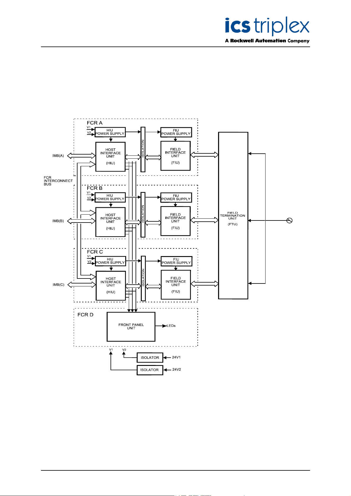
1. Description
The TMR 24V dc Digital Output module is a member of the TrustedTM range of Input/Output (I/O)
odules. All Trusted
m
all I/O modules interface to the Inter-Module Bus (IMB) which provides power and allows
communication with the TMR Processor. In addition, all modules have a field interface that is used to
connect to module specific signals in the field. All modules are Triple Modular Redundant (TMR).
M
T
/O modules share common functionality and form. At the most general level,
I
Figure 1 Module Architecture
All High Integrity I/O modules are made up of 4 sections: Host Interface Unit (HIU), the Field Interface
Unit (FIU), the Field Termination Unit (FTU), and the Front Panel Unit (or FPU).
Issue 12 Apr 10 PD-T8451 8
Page 9
Trusted
TM
Module T8451
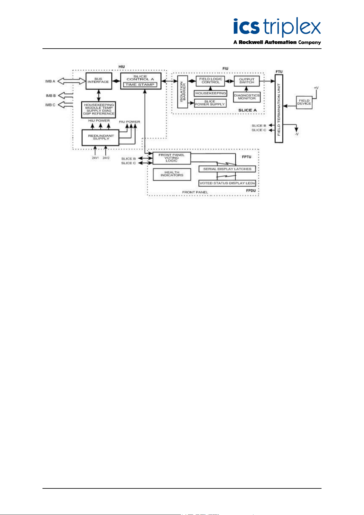
Fig 2 shows a simplified block diagram of the Trusted
M
T
24V dc Digital Output module.
Figure 2 Functional Block Diagram
1.1. Field Termination Unit (FTU)
The Field Termination Unit (FTU) is the section of the I/O module that connects all three FIUs to a
single field interface. The FTU provides the Group Fail-safe switches and passive components
necessary for signal conditioning, over-voltage protection, and EMI/RFI filtering. When installed in a
Trusted
TM
Controller or Expander Chassis, the FTU field connector interconnects to the Field I/O Cable
Assembly attached at the rear of the chassis.
The SmartSlot link is passed from the HIU to the field connections via the FTU. These signals go
directly to the field connector and maintain isolation from the I/O signals on the FTU. The SmartSlot
link is the intelligent connection between active and standby modules for co-ordination during module
replacement.
1.2. Field Interface Unit (FIU)
The Field Interface Unit (FIU) is the section of the module that contains the specific circuits necessary
to interface to the particular types of field I/O signals. Each module has three FIUs, one per slice. For
the TMR 24V dc Digital Output Module, the FIU contains one stage of the output switch structure, and
sigma-delta (JK) output circuit for each of the 40 field outputs. Two additional JK circuits provide
optional monitoring of the external field I/O supply voltage.
The FIU receives isolated power from the HIU for logic. The FIU provides additional power
conditioning for the operational voltages required by the FIU circuitry. An isolated 6.25Mbit/sec serial
link connects each FIU to one of the HIU slices.
The FIU also measures a range of on-board “house-keeping” signals that assist in monitoring the
performance and operating conditions of the module. These signals include power supply voltages,
current consumption, on-board reference voltages, board temperature, and condensation
Issue 12 Apr 10 PD-T8451 9
Page 10

Trusted
FCR Interconnect Bus between slices to vote incoming IMB data and distribute outgoing I/O
voltage and power regulation for logic
ordination during module
board
TM
Module T8451
1.3. Host Interface Unit (HIU)
The HIU is the point of access to the Inter-Module Bus (IMB) for the module. It also provides power
distribution and local programmable processing power. The HIU is the only section of the I/O module
to directly connect to the IMB backplane. The HIU is common to most high integrity I/O types and has
type dependent and product range common functions. Each HIU contains three independent slices,
commonly referred to as A, B, and C.
All interconnections between the three slices incorporate isolation to prevent any fault interaction
between the slices. Each slice is considered a Fault Containment Region (FCR), as a fault on one
slice has no effect on the operation of the other slices.
The HIU provides the following services common to the modules in the family:
• High Speed Fault-Tolerant Communications with the TMR Processor via the IMB interface.
•
module data to IMB.
• Optically isolated serial data interface to the FIU slices.
• Redundant power sharing of dual 24V dc chassis supply
power to HIU circuitry.
• Magnetically Isolated power to the FIU slices.
• Serial data interface to the FPU for module status LEDs.
• SmartSlot link between active and standby modules for co-
replacement.
• Digital Signal Processing to perform local data reduction and self-diagnostics.
• Local memory resources for storing module operation, configuration, and field I/O data.
• On-board housekeeping, which monitors reference voltages, current consumption and
temperature.
1.4. Front Panel Unit (FPU)
The Front Panel Unit (FPU) contains the necessary connectors, switches, logic, and LED indicators for
the front panel. For every module, the FPU contains the Slice Healthy, Active/Standby, the Educated
indicators (LEDs), and the module removal switches. Additional bi-colour LEDs provide status
indication for the individual I/O signals. Serial data interfaces connect the FPU to each of the HIU
slices to control the LED status indicators and monitor the module removal switches.
Issue 12 Apr 10 PD-T8451 10
Page 11

Trusted
TM
Module T8451
1.5. Line monitoring and output states
The module automatically monitors the output channel current and voltage to determine the state of
the output channel. The numerical output state and line fault status are reported back to the
application and are represented below.
Description
Field Short Circuit 5 1
Output Energized (On) 4 0
No Load, Field Open Circuit 3 1
Output De-energised (Off) 2 0
No Field Supply Voltage 1 1
Table 1 Line Monitoring Fault Status
It is recommended to fit a dummy load resistor to unused outputs to ensure a current is drawn that
exceeds the NO-LOAD threshold. This will prevent the module signalling a NO-LOAD fault.
Numerical
Output State
Line Fault
Status
1.6. Housekeeping
The output module automatically performs local measurements of several on-board signals that can be
used for detailed troubleshooting and verification of module operating characteristics. Measurements
are made within each slice’s HIU and FIU.
1.7. Fault Detection/Testing
Extensive diagnostics provide the automatic detection of module faults. The TMR architecture of the
output module and the diagnostics performed ensure the validity of all critical circuits. Using the TMR
architecture provides a Fault Tolerant method to withstand the first fault occurrence on the module and
continue normal output controls without interruption in the system or process. Faults are reported to
the user through the Healthy status indicators on the front panel of the module and through the
information reported to the TMR Processor. Under normal operations all three Healthy indicators are
green. When a fault occurs, one of the Healthy indicators will be flashing red. It is recommended that
this condition is investigated and if the cause is within the module, it should be replaced.
Module replacement activities depend on the type of spare module configuration chosen when the
system was configured and installed. The module may be configured with a dedicated Companion Slot
or with a SmartSlot for a spare replacement module.
From the IMB to the field connector, the I/O module contains extensive fault detection and integrity
testing. As an output device, most testing is performed in a non-interfering mode. Data input from the
IMB is stored in redundant error-correcting RAM on each slice portion of the HIU. Received data is
voted on by each slice. All data transmissions include a confirmation response from the receiver.
Periodically, the TMR Processor commands the onboard DSPs to perform a Safety Layer Test. The
SLT results in the DSP verifying with the TMR Processor its ability to process data with integrity. In
addition, the DSP uses Cyclical Redundancy Checks (CRC) to verify the variables and configuration
stored in Flash memory.
Between the HIU and FIU are a series of optically isolated links for data and power. The data link is
synchronized and monitored for variance. Both FIU and HIU have onboard temperature sensors to
characterize temperature-related problems. Each FIU is also fitted with a condensation sensor.
Issue 12 Apr 10 PD-T8451 11
Page 12

Trusted
TM
Module T8451
The power supplies for both the HIU and FIU boards are redundant, fully instrumented and testable.
Together these assemblies form a Power Integrity Sub System.
1.8. Sequence of Events Characteristics
The module automatically measures the field voltage and current to determine the state of each output
channel. An event occurs when the output transitions from one state to another. When a channel
changes state, the on-board timer value is recorded. When the TMR Processor next reads data from
he output module, the channel state and real-time clock value are retrieved. The TMR Processor
t
uses this data to log the state change into the system Sequence of Events (SOE) log. The user may
configure each output to be included in the system SOE log. Full details of SOE are contained in PD8013 Trusted
TM
SOE and Process Historian.
1.9. Output Switch Structure
The Digital Output Module provides a TMR switch topology where the load is driven by a total of three
fully monitored, fail-safe (6 element) switch channels, one physically resident on each OFIU in the
module. Any single switch or entire slice failure is designed to leave two of the three fail-safe switch
channels operational to power the load.
Figure 3 Output Switch Structure
The upper switches as shown in Figure 3 are denoted as N.O. (Normally Open), and are controlled by
the FIU on which they are physically resident.
Closed), and are controlled by the “upstream” neighbouring FIU.
1
The lower switches are depicted as N.C. (Normally
2
Note:
In this context, N.O. is defined as being in the off state in the absence of control signal power,
and similarly, N.C. is the on state in the absence of control signal power. These switches are
constructed from enhancement mode MOSFETs and are both guaranteed to be off in the
3
absence of module power to create gate voltage signals to bias them on
(unlike
electromechanical relays for example).
1
Their “home” FIU.
2
The home FIU, supplies an independent control signal for the “downstream” FIU FSS.
3
For an un-faulted transistor.
Issue 12 Apr 10 PD-T8451 12
Page 13

Trusted
The reason that the lower switches are specified to be on in the absence of control signal power is to
allow two channels to power the load should an entire slice fail. Even if an entire slice fails, the
surviving output circuits will carry the necessary control. The structure of each OFIU output is shown
below:
TM
Module T8451
Figure 4 Simplified Switch Circuit Diagram
A resistor provides a means of continuously monitoring the switch current. A signal transistor is used
to drive the gate of Switch 2. It provides Switch 2 with a negative gate voltage, to minimize its on
resistance, and serves to hold Switch 2 on in the event that the secondary gate control loses power.
The zener diode between the gate of Switch 2 and source is only required to protect the gate from
large voltage spikes on the drain that might capacitively couple through when Switch 1 and Switch 2
are in the off state.
The resistors in series with the gate of Switch 1 and the signal transistor serve to protect the drive logic
in the event of a malicious switch failure. The pull-up resistors define the gate voltages in the absence
of power.
1.9.1. Switch Diagnostics
During normal operation, Switch 1 and Switch 2 are maintained on. In this state, Switch 1 and Switch 2
exhibit a low resistance.
To determine the ability of the system to control the load via Switch 1 and Switch 2, their gate voltages
are modulated, one at a time. As the gate voltages are modulated, the monitoring signals
synchronously change in a predictable fashion. The local DSP analyses the relative amplitude and
phase of these small AC signals, to determine the on resistance and threshold voltages of each switch.
The current to the load does not need to be completely interrupted in order to obtain a level of
confidence in the ability of the transistors to turn off. For the TMR switch configuration in the on state,
only one fail-safe switch at a time needs to be modulated, while the other two bear the load current.
Issue 12 Apr 10 PD-T8451 13
Page 14

Trusted
TM
Module T8451
1.9.2. Short Circuit Protection Issues
In a fuse-free design such as in the Trusted
event of an over-current or over-power situation. In fact, this protection scheme offers advantages to
fuses in both automatic recovery and speed of action.
The topology of the channel provides a natural limit to the instantaneous current flow, giving the
module time to respond. Furthermore, the over-current protection circuitry is inherently self-testable,
since the threshold can be a programmable value.
The P-channel architecture of Switch 1 and Switch 2 utilizes an open-drain output structure. Under
short-circuit conditions the maximum instantaneous current with a 24V field voltage is naturally limited
to less than 5A per channel. This is because high output currents cause the gate-source voltages of
the two transistors to be reduced, tending to turn them off.
The output current is monitored by the DSP and sustained over current conditions result in a latched
over-current condition and de-energise the associated output. After removing the fault condition, the
latched over-current condition can be reset by either pressing the system fault reset button or turning
off the logical output signal to the module. The output also includes a non-replaceable fusible link for
absolute protection.
TM
System, the module is required to respond rapidly in the
1.9.3. Group Fail Safe Switches
To ensure safe operation, the output module is equipped with a series of switches that provide source
power to a group of 8 output channels. The output module Group Fail Safe Switch (GFSS) is intended
as a final control switch which can de-energise any outputs that cannot be de-energised in the normal
way. For safety, the presence of two or more faults within the output module will cause the Group Fail
Safe Switches to de-energise, resulting in all of the outputs in its group to de-energise.
There are three switches in parallel, which comprise the GFSS, one associated with each 'slice' of the
power group. The GFSS’ are controlled via a signal from one of the other two neighbouring slices.
This means that if one slice determines from the output states that an output is not in a de-energised
state when it should be, then it can command its own GFSS and those of the other slices GFSS to deenergise. This results in two of the three elements of the GFSS structure to de-energise, leaving only
one GFSS element energised. If two slices do the same thing then the last GFSS output will deenergise. For example, this would occur if two or more output switch elements fail in a 'stuck-on' state
such that the output cannot de-energise.
The GFSS control signal is generated by a charge pump driven from the comms clock to the slice
power group. If the clock fails then the GFSS bias collapses. This means that even if the ability of the
slice to communicate with a power group is lost, the GFSS can still be de-energised by stopping the
comms clock. If a slice fails, the watchdog on the HIU will time out and reset the slice, this will
shutdown the OFIU power supply and the associated GFSS control signal will also de-energise.
Issue 12 Apr 10 PD-T8451 14
Page 15

Trusted
TM
Module T8451
2. Installation
2.1. Module Insertion/Removal
CAUTION:
The module contains static sensitive parts. static handling precautions must be observed. Specifically
ensure that exposed connector pins ARE NOT TOUCHED. Under no circumstances should the
module housing BE REMOVED.
Before installation, visually inspect the module for damage. Ensure that the module housing appears
undamaged and inspect the I/O connector at the back of the module for bent pins. If the module
appears damaged or any pins are bent, do not install the module. Do not try to straighten bent pins.
Return the module for replacement.
Ensure that the module is of the correct type.
Record the module type, revision and serial number of the module before installation.
To install the module:
1. Ensure that the field cable assembly is installed and correctly located.
2. If I/O module keys are used, verify that all keys are installed in the correct positions and
properly seated in their slots.
3. Release the ejector tabs on the module using the release key. Ensure that the ejector tabs
are fully open.
4. Holding the ejectors, carefully insert the module into the intended slot.
5. Push the module fully home by pressing on the top and bottom of the module fascia.
Close the module ejectors, ensuring that they click into their locked position.
The module should mount into the chassis with a minimum of resistance. If the module does not
mount easily, do not force it. Remove the module and check it for bent or damaged pins. If the pins
have not been damaged, try reinstalling the module.
2.2. Cable Selection
I/O cables suitable for use with the TrustedTM TMR 24V dc Digital Output Module are detailed in the
following Product Descriptions.
TM
1. PD-TC200 – Trusted
2. PD-TC500 – Trusted
The Product Descriptions detailed above also detail the types of Field Termination Assembly (FTA) or
Versatile Field termination Assembly (VFTA) which may be used with type of module.
Custom length multi-core FTA cables are 0.5mm
have 4P loop impedance at 0.5A, this equates to a 2Vdc volt drop.
I/O Companion Slot Cables
TM
I/O SmartSlot Cables
2
with a resistance of 40P/km. eg a 50m cable will
2.3. Termination
Unused outputs should be commanded off in the application and wired through a 4K7 0.5W resistor to
zero volts.
Issue 12 Apr 10 PD-T8451 15
Page 16

Trusted
TM
Module T8451
2.4. Module Pinout Connections
C B A
1 Smart Slot Link C Smart Slot Link B Smart Slot Link A
2
3 Chan 5 (+) Pwr Group 1 (+) Chan 1 (+)
4 Chan 6 (+) Pwr Group 1 (+) Chan 2 (+)
5 Pwr Group 1 Rtn Pwr Group 1 (+) Pwr Group 1 Rtn
6 Chan 7 (+) Pwr Group 1 (+) Chan 3 (+)
7 Chan 8 (+) Pwr Group 1 (+) Chan 4 (+)
8
9 Chan 13 (+) Pwr Group 2 (+) Chan 9 (+)
10 Chan 14 (+) Pwr Group 2 (+) Chan 10 (+)
11 Pwr Group 2 Rtn Pwr Group 2 (+) Pwr Group 2 Rtn
12 Chan 15 (+) Pwr group 2 (+) Chan 11 (+)
13 Chan 16 (+) Pwr Group 2 (+) Chan 12 (+)
14
15 Chan 21 (+) Pwr Group 3 (+) Chan 17 (+)
16 Chan 22 (+) Pwr Group 3 (+) Chan 18 (+)
17 Pwr Group 3 Rtn Pwr Group 3 (+) Pwr Group 3 Rtn
18 Chan 23 (+) Pwr Group 3 (+) Chan 19 (+)
19 Chan 24 (+) Pwr Group 3 (+) Chan 20 (+)
20
21 Chan 29 (+) Pwr Group 4 (+) Chan 25 (+)
22 Chan 30 (+) Pwr Group 4 (+) Chan 26 (+)
23 Pwr Group 4 Rtn Pwr Group 4 (+) Pwr Group 4 Rtn
24 Chan 31 (+) Pwr Group 4 (+) Chan 27 (+)
25 Chan 32 (+) Pwr Group 4 (+) Chan 28 (+)
26
27 Chan 37 (+) Pwr Group 5 (+) Chan 33 (+)
28 Chan 38 (+) Pwr Group 5 (+) Chan 34 (+)
29 Pwr Group 5 Rtn Pwr Group 5 (+) Pwr Group 5 Rtn
30 Chan 39 (+) Pwr Group 5 (+) Chan 35 (+)
31 Chan 40 (+) Pwr Group 5 (+) Chan 36 (+)
32
Table 2 Field Connector Pinout
Issue 12 Apr 10 PD-T8451 16
Page 17

Trusted
identified below)
TM
Module T8451
2.5. TrustedTM Module Polarisation/keying.
M
All Trusted
The polarisation comprises two parts. The module and the associated field cable.
ach module type has been keyed during manufacture. The organisation responsible for the
E
integration of the Trusted
so that they correspond with the bungs fitted to the associated module prior to fitting.
T
Modules have been Keyed to prevent insertion into the wrong position within a chassis.
TM
system must key the cable by removing the keying pieces from the cable
Cable Exit
1
Polarising/Keying
Pins.
(Remove using
side cutters where
Trusted Cable
hood
12
Release button
Smart
Swap
Connector
if Fitted
Figure 5 Module polarisation
For Cables with Companion slot installations both keying strips must be polarised.
For This Module (T8451) remove keying pins 1,5,6
Issue 12 Apr 10 PD-T8451 17
Page 18

Trusted
TM
Module T8451
3. Application
3.1. Module Configuration
There is no configuration required to the physical output module. All configurable characteristics of the
module are performed using tools on the EWS and become part of the application or system.ini file
that is loaded into the TMR Processor. The TMR Processor automatically configures the output
module after applications are downloaded and during Active/Standby changeover.
The IEC1131 TOOLSET provides the main interface to configure the output module. Details of the
configuration tools and configuration sequence are provided in PD-8082B Trusted
There are three procedures necessary to configure the output module. These are:
1. Define the necessary I/O variables for the field output data and module status data using the
Dictionary Editor of the IEC1131 TOOLSET.
2. Create an I/O module definition in the I/O Connection Editor for each I/O module. The I/O
module definition defines physical information, e.g. Chassis and Slot location, and allows
variables to be connected to the I/O channels of the module.
TM
3. Using the Trusted
per-channel default or fail-safe states, and other module settings.
System Configuration Manager, define custom LED indicator modes,
TM
Toolset Suite.
3.2. T8451 Complex Equipment Definition
The T8451 I/O Complex Equipment Definition includes 8 I/O boards, referenced numerically by Rack
number:
Rack I/O Board Description Data Type Direction No. of
Channels
1 DO
2 STATE Field Output State Integer In 40
3 AI Output voltage Integer In 40
4 CI Output current Integer In 40
5 LINE_FLT Line Fault Status Boolean In 40
6 DISCREP Channel Discrepancy Integer In 3
7 HKEEPING Housekeeping Registers Integer In 57
8 INFO I/O Module Information Integer In 11
OEM Parameters - - -
Field Output Status Boolean Out 40
Table 3 Complex Equipment Definition
There are two OEM parameters included in the first rack (DO Board). These OEM parameters define
the primary module position; declaring the module’s chassis and slot location. There is no need to
define the secondary module position within the IEC1131 TOOLSET. Where systems may be required
to start-up with modules in the secondary position as the active module, e.g. primary module is not
installed when application is started, the secondary module’s position should be declared in the module
definition of the System Configuration Manager.
Issue 12 Apr 10 PD-T8451 18
Page 19

Trusted
TM
Module T8451
OEM Parameter Description Notes
TICS_CHASSIS The number of the
Trusted
TM
Chassis where
The Trusted
Trusted
TM
TM
Controller Chassis is 1, and
Expander Chassis are 2 to 15
the primary I/O module is
installed
M
TICS_SLOT The slot number in the
chassis where the primary
I/O module is installed
The I/O module slots in the Trusted
Controller chassis are numbered from 1 to 8.
The I/O Module slots in the Trusted
T
TM
Expander Chassis are numbered from 1 to 12
Table 4 OEM Parameters
3.2.1. Rack 1: DO
This board provides the connection to the logical output control signal for each of the field outputs.
Channel Description
1 Field output channel 1 logical state
2 Field output channel 2 logical state
40 Field output channel 40 logical state
Table 5 Rack 1: DO descriptions
The user application should set the output control signal to true (logic ‘1’) to turn ON or energise an
output, and false (logic ‘0’) to turn OFF or de-energise an output.
3.2.2. Rack 2: STATE
This board provides the majority voted numerical output state. This indicates the operational status of
the output channel and associated field connection.
Channel Description
1 Field output channel 1 state
2 Field output channel 2 state
40 Field output channel 40 state
Table 6 Rack 2: STATE descriptions
Issue 12 Apr 10 PD-T8451 19
Page 20

Trusted
TM
Module T8451
alue
V
escription
D
7 Channel fault
6 Field fault (e.g. field leakage to 0V or 24V)
5 Short circuit in field wiring or load
4 Output energised (ON)
3 Open circuit in field wiring or load
2 Output de-energised (OFF)
1 No field supply voltage
0 Unused
Table 7 Rack 2: STATE Output description
3.2.3. Rack 3: AI
The AI board returns the field loop voltage at the output.
Channel Description
1 Field output channel 1 voltage
2 Field output channel 2 voltage
40 Field output channel 40 voltage
Table 8 Rack 3: AI descriptions
The voltage is the median value taken from the triplicated module. The voltage level is reported as an
integer, with the units being
1
/
V. This may be used directly, scaled arithmetically or scaled using the
500
IEC1131 TOOLSET conversion tables.
To scale the value arithmetically simply divide the returned ‘integer’ by 500 to return the voltage as
either a REAL or INTEGER as required.
The IEC1131 TOOLSET conversion tables may be used to convert the value to engineering units, in
this case voltage. The full-scale range for this number format is decimal ±64, corresponding to
physical range –32000 to +32000.
Issue 12 Apr 10 PD-T8451 20
Page 21

Trusted
TM
Module T8451
3.2.4. Rack 4: CI
The CI board returns the field loop current at the output.
Channel Description
1 Field output channel 1 current
2 Field output channel 2 current
40 Field output channel 40 current
Table 9 Rack 4: CI descriptions
The current is the sum value taken from the triplicated module. The current level is reported as an
integer, with the units being
IEC1131 TOOLSET conversion tables.
To scale the value arithmetically simply divide the returned ‘integer’ by 1000 to return the current as
either a REAL or INTEGER as required.
The IEC1131 TOOLSET conversion tables may be used to convert the value to engineering units, in
this case current. The full-scale range for this number format is decimal ±32, corresponding to
physical range –32000 to +32000.
1
/
A. This may be used directly, scaled arithmetically or scaled using the
1000
3.2.5. Rack 5: LINE_FLT
Channel Description
1 Field output channel 1 line fault
2 Field output channel 2 line fault
40 Field output channel 40 line fault
Table 10 Rack 5: LINE_FLT descriptions
The line fault input state is reported as true (logic ‘1’) for a line fault condition (open circuit, short circuit,
and no field supply voltage). The logic state is the majority voted value.
3.2.6. Rack 6: DISCREP
Channel Description
1 Discrepancy status outputs 1 to 16 (output
1 is LSB)
2 Discrepancy status outputs 17 to 32
(output 17 is LSB)
3 Discrepancy status outputs 33 to 40
(output 33 is LSB)
Table 11 Rack 6: DISCREP bit descriptions
Each of the words reports the discrepancy status of 16 output channels. The corresponding bit within
the word is set to ‘1’ when a discrepancy condition is detected on that output channel’s output state
(Rack 2).
Issue 12 Apr 10 PD-T8451 21
Page 22

Trusted
TM
Module T8451
3.2.7. Rack 7: HKEEPING
Channel
Description
FCR Units (Full Scale Range)
Internal supply voltage (post regulator) -32768 32767 mV
nternal supply current (post regulator) -32768 32767 mA
I
24V2 Output Voltage -32768 32767 mV
Output voltage (post isolation) -32768 32767 mV
24V1 Output Voltage -32768 32767 mV
HIU Board Temperature
( Note: Temperature, ºC = input value / 256 )
Front Panel Load Current -32768 32767 mA
SmartSlot Link Voltage -32768 32767 mV
FIU Output Group 1 Field Supply Voltage -32768 32767 mV
FIU Board Temperature, Output Group 1
( Note: Temperature, ºC = input value / 256 )
FIU Output Group 2 Field Supply Voltage -32768 32767 mV
FIU Board Temperature, Output Group 2
( Note: Temperature, ºC = input value / 256 )
FIU Output Group 3 Field Supply Voltage -32768 32767 mV
FIU Board Temperature, Output Group 3
( Note: Temperature, ºC = input value / 256 )
FIU Output Group 4 Field Supply Voltage -32768 32767 mV
32768 32767 -
-
-32768 32767 -
-32768 32767 -
-32768 32767 -
FIU Board Temperature, Output Group 4
( Note: Temperature, ºC = input value / 256 )
FIU Output Group 5 Field Supply Voltage -32768 32767 mV
FIU Board Temperature, Output Group 5
( Note: Temperature, ºC = input value / 256 )
Diagnostic error code
-32768 32767 -
-32768 32767 -
Table 12 Rack 7: Housekeeping descriptions
Issue 12 Apr 10 PD-T8451 22
Page 23

Trusted
Each input within the housekeeping rack is reported as an integer. In general, the application engineer
will not normally require these inputs. They are provided to aid fault finding and diagnosis and may be
used for reporting and display purposes. If a slice is Fatal, then all reported housekeeping inputs are
set to zero.
TM
Module T8451
3.2.8. Rack 8: INFO
Channel Description
1 Active Module chassis number
2 Active Module slot number
3 Active Module Healthy
4 Active Module Mode
5 Standby Module Chassis Number
6 Standby Module Slot Number
7 Standby Module Healthy
8 Standby Module Mode
9 FCR Status
10 Primary module is active
11 Active module is simulated
Table 13 Rack 8: INFO descriptions
The active module chassis and slot numbers indicate the position of the currently active module.
These values will change to match the primary or secondary module position, depending on their active
status, i.e. active/standby changeover will “swap” the values for the active module chassis and slot
number channels with those in the standby module chassis and slot number channels. The chassis
and slot numbers are set to zero if the module is not present.
The Active and Standby module healthy channel is returned as an integer, however only the least
significant bit is used. A value of 0 indicates that a fault has been detected, a non-zero value indicates
that the module is healthy.
The Active and Standby Module Mode is an integer indicating the current operating mode of the
associated module. The value indicates the current internal operating mode of the module.
Value Module Mode
5 Shutdown
4 Maintain
3 Active
2 Standby
1 Configuration
0 Unknown, no module present
Table 14 Rack 8 INFO bit descriptions
Issue 12 Apr 10 PD-T8451 23
Page 24

Trusted
The FCR Status channel reports the fault status of the active and standby modules. The value is bitpacked as shown below, the least significant byte is used with the most significant 8-bits set to zero:
The ‘Primary Module is active’ channel is set to non-zero if the primary module is the current active
module, i.e. the active module is in the chassis and slot numbers defined within the OEM parameters.
The ‘Active Module is simulated’ channel is set to non-zero if the active module is being simulated, this
will only be set if the module is not present or the simulation enable has been set within the module’s
configuration in the system.ini file.
TM
Module T8451
Bit
7 6 5 4 3 2 1 0
Standby Module Active Module
Ejector
open
FCR C
Healthy
FCR B
Healthy
Table 15 Rack 8: FCR bit descriptions
FCR A
Healthy
Ejectors
open
FCR C
Healthy
FCR B
Healthy
FCR A
Healthy
3.3. Sequence of Events Configuration
Each Boolean Output Variable can be configured for automatic Sequence of Events (SOE) logging.
This applies to the Output Status and Line Fault Status variables. A Boolean variable is configured for
SOE during the variable definition in the Data Dictionary Editor. To select SOE, press the Extended
Button in the Boolean Variable Definition Dialog Box to open the Extended Definition Dialog. Then
check to box for Sequence of Events to enable the variable for automatic SOE logging.
During operation, the output module automatically reports time-stamped change of state information
for the output data. The TMR Processor automatically logs change of state for configured SOE
variables into the system SOE Log. The SOE Log can be monitored and retrieved using the SOE and
Process Historian Package running on the EWS. This software package is described in PD-8013.
3.4. SYSTEM.INI File Configuration
There are many operating characteristics of the output module that can be customised for a particular
application. The System Configuration Manager is a tool that allows the user to configure the specific
operating characteristics for each module. Descriptions of the items that may be configured for the
Trusted
Certain characteristics apply to the entire module and are considered Module Configurable Items.
Other characteristics apply to individual output channels and are considered Channel Configurable
Items. There are specific default settings for each of the configurable items. If the default settings are
appropriate for a given application, then customization of the module definition in the System
Configuration Manager is not required.
In order for De-energising short circuit detection to function a template is required. The template will
allow individual channels to be set to either detect or not a short circuit (less than a nominal 20 ohms
for Level 1 hardware builds or a nominal 10 ohms for level 2 builds).
TM
24V dc Digital Output Module T8451 are contained in PD-8082B.
Issue 12 Apr 10 PD-T8451 24
Page 25

Trusted
T8451 Trusted TMR 24Vdc Digital Output
TM
Module T8451
4. Operation
4.1. Front Panel
Status indicators on the front panel of the module provide visual indications of the module’s operational
status and field output status. Each indicator is a bicolour LED. Located at the top and bottom of each
module is an ejector lever that is used to remove the module from the chassis. Limit switches detect
the open/closed position of the ejector levers. The ejector levers are normally latched closed when the
module is firmly seated into the Controller or Expander Chassis.
Module
Latch
Module
Status
Indicators
Output
Status
Indicators
Module
Latch
Figure 6 Module Front Panel
Issue 12 Apr 10 PD-T8451 25
Page 26

Trusted
TM
Module T8451
4.2. Module Status LEDs
There are six module status indicators on the module front panel: three Healthy, one Active, one
Standby, and one Educated. The Healthy indicators are controlled directly by each module slice. The
Active, Standby, and Educated indicators are controlled by the FPU. The FPU receives data from
each of the module slices. The FPU performs a 2-oo-3 vote on each data bit from the slices and sets
the indicators accordingly.
The module status indicator modes and their meanings are described as follows:
INDICATOR STATE DESCRIPTION
Healthy Off No power applied to the module.
Amber Slice is in the start-up state (momentary after
installation or power-up)
Green Slice is healthy.
Red – flashing Fault present on the associated slice but the slice is still
operational.
Red (momentary) On installation – power applied to the associated slice.
Red The associated slice is in the fatal state. A critical fault
has been detected and the slice disabled..
Active Off Module is not in the Active state.
Green Module is in the Active (or Maintain) state.
Red – flashing Module is in the shutdown state if the Standby LED is
off.
Red – flashing Module is in the fatal state if the Standby LED is also
flashing.
Standby Off Module is not in the Standby state.
Green Module is in the Standby state.
Red – flashing Module is in the fatal state. The Active LED will also be
flashing red.
Educated Off Module is not educated.
Green Module is educated.
Green – flashing Module is recognised by the Processor but education is
not complete.
Amber - Flashing Active/standby changeover in progress
Table 16 Module Status LEDs
Issue 12 Apr 10 PD-T8451 26
Page 27

Trusted
TM
Module T8451
4.3. I/O Status Indicators
There are 40 output channel status indicators on the module front panel, one for each field output.
These indicators are controlled by the FPU. The FPU receives data from each of the module slices.
The FPU performs a 2-oo-3 vote on each data bit from the slices and sets the indicators accordingly.
The output status indicator mode is dependent upon the numerical state of the output channel. Each
output state can be defined to have a particular indicator mode: off, green, red, flashing green, or
flashing red.
The configurable indicator modes allow users to customise the output status indications to suit
individual application requirements. Without customisation, the default indicator modes are suitable for
line-monitored digital output devices as described below:
INDICATOR STATE DESCRIPTION
Off Output is Off.
Green Output is On.
Green – flashing No Load, output open circuit.
Red Field short circuit, output over current protection triggered and output
channel is latched off.
Red – flashing Channel fault, or no field supply voltage
Table 17 I/O Status LEDs
Note: The LEDs indicating channel status may be configured to suit user requirements by
implementing the procedure for configuring the System.INI file detailed in PD-8082B.
Issue 12 Apr 10 PD-T8451 27
Page 28

Trusted
TM
Module T8451
5. Fault Finding and Maintenance
5.1. Fault Reporting
Output module faults are reported to the user through visual indicators on the front panel of the module
and through status variables which may be automatically monitored in the application programs and
external system communications interfaces. There are generally two types of faults that must be
remedied by the user: external wiring and module faults. External wiring faults require corrective action
in the field to repair the fault condition. Module faults require replacement of the output module.
5.2. Field Wiring Faults
By measuring the output channel voltage and current, the module automatically detects field-wiring and
load faults. When a field signal fails open circuit, short circuit or there is not field supply voltage
connected, the output status indicator will display the configured LED mode, the corresponding output
state will be reported and the line fault status for that channel will be set to ‘1’. All other output
channels will be unaffected, except in the case of common cause wiring and supply voltage faults in
the field.
The field output voltage and current variables can be monitored to determine the actual operating
conditions of each output channel. This additional information assists the user in determining the
specific type of wiring fault.
Once the specific field-wiring fault has been identified and corrected, the output status variables and
output status indicator will display the normal on/off status of the field device.
5.3. Module Faults
Extensive diagnostics provide the automatic detection of module faults. The TMR architecture of the
output module and the diagnostics performed ensure the validity of all critical circuits. Using the TMR
architecture provides a Fault Tolerant method to withstand the first fault occurrence on the module and
continue normal output controls without interruption in the system or process. Faults are reported to
the user through the Healthy status indicators on the front panel of the module and through the INFO
and HKEEPING variables. Under normal operations all three Healthy Indicators are green. When a
fault occurs, one of the Healthy Indicators will be flashing red. It is recommended that this condition is
investigated and if the fault is within the module, it should be replaced.
Module replacement activities depend on the type of spare module configuration chosen when the
system was configured and installed. The module may be configured with a Dedicated Standby Slot or
with a SmartSlot for a spare replacement module.
Issue 12 Apr 10 PD-T8451 28
Page 29

Trusted
TM
Module T8451
5.4. Companion Slot
M
For a Companion Slot configuration, two adjacent slots in a Trusted
same Output module function. One slot is the primary slot and the other a unique secondary (or spare)
slot. The two slots are joined at the rear of the Trusted
M
T
Chassis with a double-wide I/O Interface
T
Chassis are configured for the
Cable that connects both slots to common field wiring terminations. During normal operations, the
primary slot contains the active module as indicated by the Active indicator on the front panel of the
module. The secondary slot is available for a spare module that will normally be the standby module
as indicated by the Standby indicator on the front panel of the module.
Depending on the installation, a hot-spare module may already be installed, or a module blank will be
installed in the standby slot. If a hot-spare module is already installed, transfer to the standby module
occurs automatically when a module fault is detected in the active module. If a hot spare is not
installed, the system continues operating from the active module until a spare module is installed.
De-energised short-circuit templates are only supported on the newer 3.3V modules, and not on the
earlier 5V modules. If a module has been configured with a de-energised short circuit template and an
attempt is made to swap to a 5V module, the swap may appear to be successful but the standby
module has actually rejected the swap. 5V modules have hardware revisions A to D for 8451.
5.5. SmartSlot
For a SmartSlot configuration, the secondary slot is not unique to each primary slot. Instead, a single
secondary slot is shared among many primary slots. This technique provides the highest density of
modules to be fitted in a given physical space. At the rear of the Trusted
TM
Chassis, a single-wide I/O
Cable connects the secondary slot directly to the I/O Cable connected to the failed primary module.
With a spare module installed in the SmartSlot and the SmartSlot I/O Cable connected to the failed
primary module, the SmartSlot can be used to replace the failed primary module.
Output module Slot Jumper cable TC-308-02
Smart Slot between chassis can be performed if the chassis are version 2 (or higher). These chassis
have the connector fitted to enable connection of a TC-006 that ensures the 0 Volt of each chassis is
at the same potential.
5.6. Cold Start
If an I/O module has shut down (due, for example, to two existing faults), the three Healthy LEDs will
be red, the Active and Standby LEDs will be flashing red and the Educated LED will be flashing amber.
The I/O functions provided by this module will have been lost if a hot swap partner has not taken over
control. The module can only be restarted by removing it from its slot and re-inserting it.
If an I/O module is inserted into a functional system slot which previously had no active module (e.g.
removing and reinserting as above), then the processor will educate the module once it has booted.
Once educated, the Educated LED will be steady green and the Active LED will be red flashing.
Input modules will now be reading and reporting their inputs. Output modules have not yet energised
their outputs. To activate outputs and to set the module’s Active LED and the processor’s System
Healthy LED steady green, press the processor Reset pushbutton.
Issue 12 Apr 10 PD-T8451 29
Page 30

Trusted
The user must define the primary, and optionally the secondary, I/O module location for each
nique and is defined as part of the
. Secondary module locations
can be unique or shared between multiple secondary modules and are defined within the
system will automatically determine the
up, if the primary module is installed, it will become the active module by default.
efined within the System.INI file and no primary module is
present, and if the secondary module location is unique, the secondary module will become
the active module by default. If the secondary module is installed with no primary module
secondary module location is not unique (as in a SmartSlot configuration),
In order for a module to become the active module, the TMR Processor will verify that the
ype and that both Module Removal switches are closed. At
ill be informed. Once it
An active/standby changeover starts with the TMR Processor checking to see if a standby I/O
available, the TMR Processor will continue to
utilise the active module and will continue to check for an available standby I/O module. Once a
standby module is found, the TMR Processor will verify that the I/O module is of the correct type,
dule Removal switches are closed, and that the I/O module is a part of the correct
module pair by using the SmartSlot link. At this point, the TMR Processor will configure the
ive I/O module
and place the standby I/O module into the standby state. The active module is then placed in the
maintain state (which suspends field loop testing), and any module specific changeover data is
efore the active/standby changeover takes place,
to indicate transfer of dynamic change over data (COD). The previous standby module then
becomes the active module and the original module becomes standby. If the currently active
tests, the TMR Processor will revert it to the
standby state, and the module in the maintain state will revert back to the active state. When both
status,
TM
Module T8451
5.7. Transfer between Active and Standby Modules
The TMR Processor is responsible for managing a pair of I/O modules through an active/standby
changeover. The following rules apply to active/standby changeovers, though the TMR Processor and
not the I/O module enforce them:
•
I/O module pair. Each primary module location must be u
complex equipment definition within the IEC1131 TOOLSET
module’s section within the System.INI file. The
secondary module position if the primary module is installed and is operable.
• On initial startIf the secondary module has been d
present, and the
then NO module for that module pair will become active.
•
module is the correct I/O module t
this point the I/O module is configured and eventually placed in the active state.
• A module in the active state should never be removed.
• When a fault occurs on the active module, the TMR Processor w
becomes aware of the fault, the TMR Processor will attempt an active/standby changeover.
module is installed. If no standby I/O module is
that both Mo
standby I/O module with the same configuration information as the currently act
transferred. The educated light flashes amber b
module does not successfully complete the self-
Module Removal switches are opened on an active module, regardless of the module fault
the TMR Processor will treat it as a request to perform an active/standby changeover.
Under normal conditions, an active/standby changeover will only occur if the new active module is
fault-free. Under some circumstances, it is desirable to be able to force a changeover to a known
faulted module. This can be accomplished by opening the Module Removal switches on the currently
active module and pressing the push-button reset on the TMR Processor. This will force the
changeover to proceed even if the new active module is not fault free.
Issue 12 Apr 10 PD-T8451 30
Page 31

Trusted
TM
Module T8451
6. Specifications
System Supply Voltage Range 20 to 32Vdc
Circuit Type Fault tolerant, fully triplicated with optional
line monitoring
Number of Outputs 40 Channels
Independent Power Groups 5 each of 8 outputs
Operational Output/Field Voltage Range 18 to 32V dc
Output Voltage
Measurement Range 0 to 32V dc
Maximum Withstanding -1 to 40V dc
Output Current Rating (Continuous) 2A per channel
Maximum capacitance Pre release 3.5: 30-55uF
Flashing/pulsing current loads Release 3.5 is recommended
Minimum On State Load Current 50mA
Output Off State Resistance (effective
leakage)
Output On State resistance 0.6P
Output Short Circuit Protection Electronic (latching)
Channel to Channel Crosstalk >-40dB
Power Consumption
Field Supply (1A per channel)
System Supply (24V)
Field Common Isolation
Sustained Working
Maximum Withstanding
Output Turn-on/off Delay 0.5ms
Sample Update Time 0.5ms
Sequence of Events
Event Resolution
Self-Test Interval 2 minutes
Intrinsic Safety External barrier
Output Short Circuit Protection Automatic
Operating Temperature
Non-operating Temperature
Temperature change 0.5ºC/min
Operating Humidity 5 – 95% RH non-condensing
Environmental Specifications Refer to Document 552517
Dimensions
Height
Width
Depth
Weight 1.3kg (2.7lbs)
limited to 8A per power group
Release 3.5: at least 2800uF at 2A
33kP
24W
24W
±250V dc
±2.5kV dc
1ms
-5°C to 60°C (23°F to 140°F)
-25°C to 70°C (-13°F to 158°F)
266mm (10.5ins)
31mm (1.2ins)
303mm (12ins)
Issue 12 Apr 10 PD-T8451 31
Page 32

 Loading...