

Page 1

TrustedTM
PD-T8110B/T8110
TM
Trusted
TMR Processor
Introduction
The TrustedTM Processor forms the main processing element in a TrustedTM system, providing overall
system control and monitoring facilities.
M
T
A powerful, user-configurable module, the Trusted
through a variety of analogue and digital I/O modules via a Trusted
TM
The range of applications for the Trusted
gas control, emergency shutdown, monitoring and control, and turbine control.
TMR Processor vary in integrity level and include fire and
TMR Processor processes input and output data
TM
TMR Communications bus.
Features
• Triple Modular Redundant (TMR), fault tolerant (3-2-0) operation
• Hardware Implemented Fault Tolerant (HIFT) architecture
• Dedicated hardware and software test regimes which provide very fast fault
recognition and response times
• Automatic fault handling without nuisance alarming
• Time-stamped fault historian
• Hot replacement (no need to re-load programs)
• Full suite of IEC 1131-3 programming languages
• Front panel indicators that show module health and status
• Front panel RS 232 serial diagnostics port for system monitoring,
configuration and programming.
• IRIG-B002 and 122 time synchronisation signals ( Available on T8110B only )
• Active and Standby processor fault and failure contacts
• Two RS422 / 485 configurable 2 or 4 wire connections ( Available on T8110B
only )
• One RS485 2 wire connection ( Available on T8110B only )
3V Certified IEC 61508 SIL 3
• T
Issue 18 Feb 08 PD-T8110B/T8110 1
Page 2

Trusted
Issue Record
Issue
Number Date Revised by Technical CheckAuthorised by Modification
11 Oct 05 J W Clark Format
12 Aug 06 N Owens I Vince P Stock Corrections
13 Sep 06 N Owens I Vince P Stock 3.5 Scan Time Calc
14 Nov 06 N Owens I Vince P Stock Specifications
15 Dec 06 N Owens I Vince P Stock I/O Definition
16 Mar 07 N Owens I Vince P Stock Hot Swap
TM
TMR Processor T8110B/T8110
17 Sep 07 N Owens I Vince P Stock Max Scan Time
18 Feb 08 N Owens A Holgate P Stock TTMRP_0 scaling
Issue 18 Feb 08 PD-T8110B/T8110 2
Page 3

Trusted
TM
TMR Processor T8110B/T8110
This page is intentionally blank
Issue 18 Feb 08 PD-T8110B/T8110 3
Page 4

Trusted
TM
TMR Processor T8110B/T8110
Table of Contents
1. Description...................................................................................................................................8
1.1. Overview......................................................................................................................................8
1.2. Hardware Implemented Fault Tolerant (HIFT) Clock...................................................................9
1.3. Power Distribution........................................................................................................................9
2. Installation..................................................................................................................................10
2.1. Module Insertion/Removal .........................................................................................................10
2.2. PCBs and Connectors ...............................................................................................................10
2.3. Module Pinout Connections .......................................................................................................11
2.3.1. External I/O Connector (PL1) ....................................................................................................11
3. Application .................................................................................................................................12
3.1. Module Configuration.................................................................................................................12
3.1.1. Updater Section .........................................................................................................................12
3.1.2. Security Section.........................................................................................................................12
3.1.3. ICS2000 Section........................................................................................................................12
3.1.4. System Section..........................................................................................................................12
3.1.5. ISaGraf Configuration section....................................................................................................16
3.1.6. Chassis Section .........................................................................................................................16
3.1.7. InterRange Instrumentation Group. (IRIG) ................................................................................16
3.1.8. Additional User Serial Ports.......................................................................................................17
3.2. Complex I/O Equipment Definition.............................................................................................18
I/O Complex Equipment ‘...........................................................................................................18
3.2.1. TTMRP’......................................................................................................................................18
3.3. Inter-Module Bus........................................................................................................................21
3.3.1. Processor Memory Voting Bus ..................................................................................................21
3.3.2. Inter-Module Bus Voting Bus .....................................................................................................21
3.3.3. Processor Voting Bus ................................................................................................................21
3.3.4. Front Panel Voting Bus..............................................................................................................22
3.4. Isolation......................................................................................................................................22
4. Operation...................................................................................................................................23
4.1.1. System Overheads ....................................................................................................................24
4.1.2. On-Line Operator Inputs ............................................................................................................24
4.2. Standby Processor.....................................................................................................................24
4.3. Module Management .................................................................................................................24
4.4. Security......................................................................................................................................24
4.5. Front Panel ................................................................................................................................25
4.6. Module Status LEDS..................................................................................................................26
4.6.1. Reset Button ..............................................................................................................................27
Issue 18 Feb 08 PD-T8110B/T8110 4
Page 5

Trusted
4.6.2. Maintenance Enable Keyswitch.................................................................................................27
4.7. Composite Scan Time Estimation (pre TÜV release 3.5)..........................................................27
4.7.1. Central Modules.........................................................................................................................27
4.7.2. Input Modules ............................................................................................................................28
4.7.3. Output Modules..........................................................................................................................28
TM
TMR Processor T8110B/T8110
.7.4.
4
4.7.5. Composite Scan Time ...............................................................................................................29
4.7.6. Example Calculation ..................................................................................................................30
4.8. Composite Scan Time Estimation (from TÜV release 3.5)........................................................31
4.8.1. Input modules ............................................................................................................................31
4.8.2. Output Modules..........................................................................................................................31
4.8.3. Application Execution.................................................................................................................32
4.8.4. Communications ........................................................................................................................32
4.8.5. Example Calculation ..................................................................................................................33
5. Fault Finding and Maintenance..................................................................................................34
5.1. Testing and Diagnostics ............................................................................................................34
5.2. Faults .........................................................................................................................................34
5.3. Transfer between Active and Standby Processor Modules .......................................................35
6. Specifications.............................................................................................................................36
pplication Execution.................................................................................................................29
A
Figures
Figure 1 Module Architecture....................................................................................................................8
Figure 2 Functional Block Diagram showing TrustedTM TMR Processor Communications ...................22
Figure 3 Block Diagram of Module Operation ........................................................................................23
Figure 4 Module Front Panel ..................................................................................................................25
Tab le s
Table 1 External I/O Connector Pin-Out.................................................................................................11
Issue 18 Feb 08 PD-T8110B/T8110 5
Page 6

Trusted
TM
TMR Processor T8110B/T8110
Notice
The content of this document is confidential to ICS Triplex Technology Ltd. companies and their
partners. It may not be given away, lent, resold, hired out or made available to a third party for any
purpose without the written consent of ICS Triplex Technology Ltd.
This document contains proprietary information that is protected by copyright. All rights are reserved.
Microsoft, Windows, Windows 95, Windows NT, Windows 2000, and Windows XP are registered
trademarks of Microsoft Corporation.
The information contained in this document is subject to change without notice. The reader should, in
all cases, consult ICS Triplex Technology Ltd. to determine whether any such changes have been
made. From time to time, amendments to this document will be made as necessary and will be
distributed by ICS Triplex Technology Ltd.
Information in this documentation set may be subject to change without notice and does not represent
a commitment on the part of ICS Triplex Technology Ltd.
The contents of this document, which may also include the loan of software tools, are subject to the
confidentiality and other clause(s) within the Integrator Agreement and Software License Agreement.
No part of this documentation may be reproduced or transmitted in any form or by any means,
electronic or mechanical, including photocopying and recording, for any purpose, without the express
written permission of ICS Triplex Technology Ltd.
Disclaimer
The illustrations, figures, charts, and layout examples in this manual are intended solely to illustrate the
text of this manual.
The user of, and those responsible for applying this equipment, must satisfy themselves as to the
acceptability of each application and use of this equipment.
This document is based on information available at the time of its publication. While efforts have been
made to be accurate, the information contained herein does not purport to cover all details or variations
in hardware or software, nor to provide for every possible contingency in connection with installation,
operation, or maintenance. Features may be described herein which are present in all hardware or
software systems. ICS Triplex Technology Ltd. assumes no obligation of notice to holders of this
document with respect to changes subsequently made.
ICS Triplex Technology Ltd. makes no representation or warranty, expressed, implied, or statutory with
respect to, and assumes no responsibility for the accuracy, completeness, sufficiency, or usefulness of
the information contained herein. No warranties of merchantability or fitness for purpose shall apply.
Issue 18 Feb 08 PD-T8110B/T8110 6
Page 7

Trusted
TM
TMR Processor T8110B/T8110
Revision and Updating Policy
All new and revised information pertinent to this document shall be issued by ICS Triplex Technology
Ltd. and shall be incorporated into this document in accordance with the enclosed instructions. The
change is to be recorded on the Amendment Record of this document.
Precautionary Information
WARNING
Warning notices call attention to the use of materials, processes, methods, procedures or limits which
must be followed precisely to avoid personal injury or death.
CAUTION
Caution notices call attention to methods and procedures which must be followed to avoid damage to
the equipment.
Notes:
Notes highlight procedures and contain information to assist the user in the understanding of the
information contained in this document
Warning
RADIO FREQUENCY INTERFERENCE
Most electronic equipment is influenced by Radio Frequency Interference (RFI). Caution should be
exercised with regard to the use of portable communications equipment around such equipment.
Signs should be posted in the vicinity of the equipment cautioning against the use of portable
communications equipment.
MAINTENANCE
Maintenance must be performed only by qualified personnel, otherwise personal injury or death, or
damage to the system may be caused.
Caution
HANDLING
Under no circumstances should the module housing be removed.
Associated Documents
Product Descriptions (PD) provide product specific information.
The Safety Manual contains the recommended safety requirements for the safety system design.
The PD8082B – Toolset Suite provides specific guidance on system configuration and application
generation.
The Operator and Maintenance Manual contains general guidelines on maintenance and diagnostic
procedures.
For technical support email: support@icstriplex.com
Issue 18 Feb 08 PD-T8110B/T8110 7
Page 8
Trusted
TM
TMR Processor T8110B/T8110
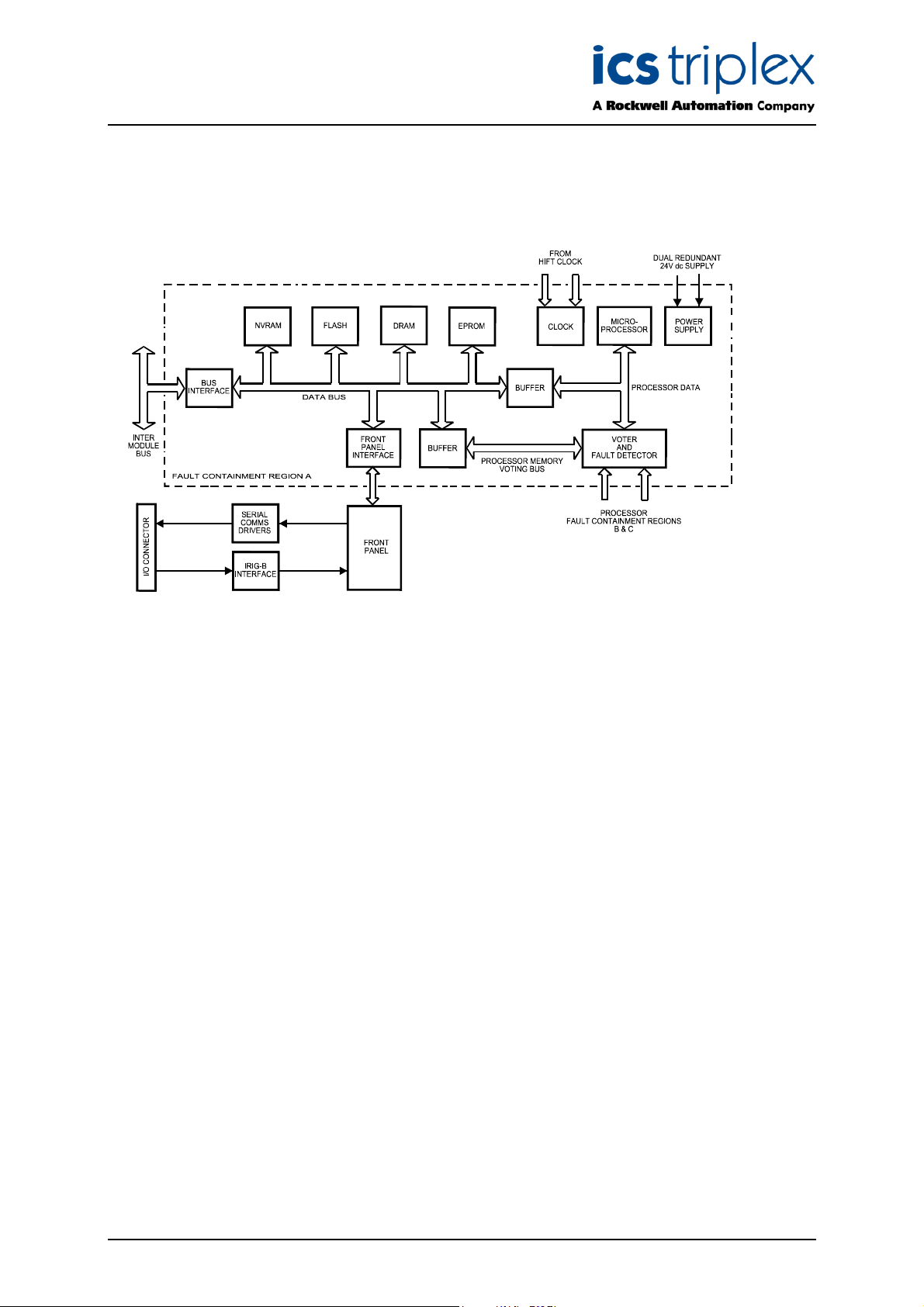
1. Description
Figure 1 Module Architecture
1.1. Overview
The TrustedTM TMR Processor is a fault tolerant design based on a TMR architecture arranged in a
lock-step configuration. Figure 1 shows, in simplified terms, the basic structure of the Trusted
Processor module.
The module contains three processor fault containment regions (FCR), each containing a Motorola
Power PC series processor and its associated memory (EPROM, DRAM, Flash ROM, and NVRAM),
memory mapped I/O, voter and glue logic circuits. Each processor FCR has voted two-out-of-three (2oo-3) read access to the other two processor FCRs memory systems to eliminate divergent operation
The module’s three processors store and execute the application program, scan and update the I/O
modules and detect system faults. Each processor executes the application program independently,
but in lock-step synchronisation with the other two. Should one of the processors diverge, additional
mechanisms allow the failed processor to re-synchronise with the other two.
Each processor has an interface with the Inter-Module Bus which consists of an input voter,
discrepancy detector logic, memory and an output driver. The output of each processor is connected
by the module connector to a different channel of the triplicated Inter-Module Bus.
TM
Communication between the Trusted
Trusted
Expander Interface to a Expander chassis.
TM
Interface module, such as the TrustedTM TMR Interface to a Regent+Plus I/O chassis, or an
TMR Processor and modules in other chassis is via either a
TM
TMR
Issue 18 Feb 08 PD-T8110B/T8110 8
Page 9

Trusted
TM
TMR Processor T8110B/T8110
The functions of the four types of module memory are:
EPROM
Flash ROM
DRAM
NVRAM
- Holds module bootstrap loader
- Stores module firmware and the application program
- Working memory with scaleable capacity
- Holds data such as event logs and retained program data.
Note: The NVRAM provides data retention for up to 10 years.
The front panel comprises a Fault Containment Region (FCR D) separate from the other FCRs and
contains non-critical simplex functions. These include the diagnostics port and maintenance enable
keyswitch mounted on the front panel of the Processor. Other functions within the front panel FCR are
the serial communications drivers and the IRIG-B interface. These are accessed though the I/O
connector via adaptor units at the rear of the Processor. The Processor and front panel FCR
participate in all module voting operations.
Two IRIG-B input standards are available to the Processor; IRIG-B002 and IRIG-B122. The standard
used by the Processor is controlled by software setting a flag in the memory. The IRIG-B signals are
used to synchronise systems and time-stamp entries in the Sequence of Events (SOE) log.
Three serial communications are available from the 4-channel UART. These are detailed as follows:
1. Channel 0 Front Panel Diagnostic Port (RS232)
2. Channel 1 Not configured
3. Channel 2 Communications Serial Port 2 (RS422/485)
4. Channel 3 Communications Serial port 3 (RS422/485)
TM
The Trusted
OPERATING SYSTEM (TrustedTM OS) is used in support of the Motorola Power PC series
processor architecture. The real time kernel is a high speed, high functionality kernel made for faulttolerant distributed systems. The distributed communication is made transparent over all processors.
The kernel provides basic services (such as basic memory management), and interference free
software environments which allow software of various integrity levels to reside and co-operate in a
single processing environment.
An Application Program Interface (API) provides a consistent run-time interface for the services
provided by the Trusted
same function to system-specific software executing within the Trusted
TM
TMR Processor to the application program. The API also performs the
TM
TMR Processor.
1.2. Hardware Implemented Fault Tolerant (HIFT) Clock
Each of the Processor and front panel fault containment regions has its own HIFT clock, which are
provided with a synchronisation reference signal from the fault-tolerant reference clocks.
1.3. Power Distribution
Each of the Processor and FCRs derive their internal voltages from dual redundant +24V dc power
supplied via the module connector from the Trusted
TM
Controller chassis backplane.
Issue 18 Feb 08 PD-T8110B/T8110 9
Page 10

Trusted
TM
TMR Processor T8110B/T8110
2. Installation
2.1. Module Insertion/Removal
CAUTION:
The module contains static sensitive parts. Static handling precautions must be observed. Specifically
ensure that exposed connector pins ARE NOT TOUCHED. Under no circumstances should the
module housing BE REMOVED.
Before installation, visually inspect the module for damage. Ensure that the module housing appears
undamaged and inspect the I/O connector at the back of the module for bent pins. If the module
appears damaged or any pins are bent, do not install the module. Do not try to straighten bent pins.
Return the module for replacement.
Ensure that the module is of the correct type.
Record the module type, revision and serial number of the module before installation.
To install the module:
1. Ensure that the field cable assembly is installed and correctly located.
2. Release the ejector tabs on the module using the release key. Ensure that the ejector tabs
are fully open.
3. Holding the ejectors, carefully insert the module into the intended slot.
4. As soon as the front panel LEDS illuminate, push the module fully home by pressing on the
top and bottom of the module fascia. The module should be inserted promptly to ensure that
it connects to the Interface Adapter before reading the licenses.
5. Close the module ejectors, ensuring that they click into their locked position.
The module should mount into the chassis with a minimum of resistance. If the module does not
mount easily, do not force it. Remove the module and check it for bent or damaged pins. If the pins
have not been damaged, try reinstalling the module.
2.2. PCBs and Connectors
The TrustedTM TMR Processor comprises five separate PCB assemblies:
1. Three identical processor boards
2. One Riser board to provide the connection between the PCB assemblies
3. One module Main board that provides the Inter-Module bus connection and front panel
facilities.
Issue 18 Feb 08 PD-T8110B/T8110 10
Page 11
Trusted
TM
TMR Processor T8110B/T8110
2.3. Module Pinout Connections
2.3.1. External I/O Connector (PL1)
This connector provides a number of discrete input and outputs. These are provided to allow the
Trusted
M
T
TMR Processor status to be monitored by external hardware, and to allow the Trusted
M
T
TMR Processor to monitor the power supply status signals. The connector also provides access to the
communications ports and connections for IRIG-B input signals. To enable the communications ports
and IRIG-B facilities to be accessed, the user must install the following:
1. Processor Interface Adaptor T8120 for the communications ports.
2. Processor Interface Adaptor Unit (IRIG-B) T8121 for both communications ports and
IRIG-B facilities
Note: IRIG B and serial facilities are only available on the T8110B
PL1 is a 48-way DIN41612 E type connector.
Row
Pin A C E
2 Fault relay (NC) DIAG_RTN Failed relay (NC)
4 Fault relay (common) DIAG_IN_1 Failed relay (common)
6 Fault relay (NO) 0V Port 1 Failed relay (NO)
8 Not Connected Serial Port 1 B Not Connected
10 5V_D Serial Port 1 A IRIG-B122+
12 DATA_OUT 0V Port 2 IRIG-B12214 ENABLE Serial Port 2 B TX Reserved
16 DATA_IN Serial Port 2 A TX Reserved
18 CLK Serial Port 2 B RX/TX IRIG-B00220 0V Serial Port 2 A RX/TX IRIG-B002+
22 Chassis GND 0V Port 3 Chassis GND
24 Chassis GND Serial Port 3 B TX Chassis GND
26 Chassis GND Serial Port 3 A TX Chassis GND
28 24V PSU 1 LV Warning Serial Port 3 B RX/TX 24V PSU 1 Fail
Shutdown
30 24V PSU 2 LV Warning Serial Port 3 A RX/TX 24V PSU 2 Fail
Shutdown
32 24V Return 24V Return 24V Return
Table 1 External I/O Connector Pin-Out
Issue 18 Feb 08 PD-T8110B/T8110 11
Page 12

Trusted
TM
TMR Processor T8110B/T8110
3. Application
3.1. Module Configuration
The TrustedTM TMR Processor requires no hardware configuration.
M
Every Trusted
given in PD-8082B (Trusted
slot of the processor chassis by default. The System Configurator allows the selection of options on
ports, IRIG and system functions. The use of the System Configurator is described in PD-8082B. The
options are described below.
3.1.1. Updater Section
T
system requires a System INI Configuration file. Details of how to design this are
TM
Toolset Suite). The configuration has a processor assigned to the left
If Auto Protect Network Variables is selected, this configures the TrustedTM System to use a reduced
Modbus Protocol map. See product description PD-8151B (Trusted
TM
Communication Interface
Module) for further details.
Inter Group Delay equates to the Modbus update cycle. This is the minimum period between
successive Modbus update messages sent to each of the Communications Interface modules. The
default value (as shown) is 50ms which provides a compromise between latency and performance.
Adjustment is made in 32 integer ms increments, i.e. a value of 33 will equal 64ms as will 64.This may
be increased or decreased as required, however since only one update message is sent per
application scan, and an application scan may often be more than 50ms, there is little benefit in
adjusting this variable.
3.1.2. Security Section
The above display is also used to configure a password allowing the user to interrogate a Trusted
System using the Windows-based HyperTerminal facility or a similar terminal program. The password
is configured by selecting the New Password button and entering the new password twice in the
displayed dialogue box.
TM
3.1.3. ICS2000 Section
This section only applies to TrustedTM systems connected via a Trusted to ICS2000 Interface Adapter
to an ICS2000 system. This allows the data sources for the three mimic tables to be selected. Please
refer to your Trusted
TM
supplier for further information.
3.1.4. System Section
WARNING
Changes made to the System Section may affect System performance, Fault Detection times and
violate the process safety tolerances.
Entries to this section are typed directly into the SYSTEM Section text window.
Definitions
NIO Module = Native Input or Output (I/O) Module. This refers to all I/O modules resident in a
Trusted
TM
chassis. It does not refer to I/O modules resident in other chassis types and communicating
via a bridge interface module.
Dual I/O = Module using two voted circuits to connect to a field device.
TMR I/O = Module using three voted circuits to connect to a field device.
Issue 18 Feb 08 PD-T8110B/T8110 12
Page 13

Trusted
TM
rim_interval
TMR Processor T8110B/T8110
The value is specified in milliseconds. It specifies the minimum amount of time that must elapse
etween polls of Trusted
b
M
T
MR Interface modules.
T
Changes to this value are reflected by the system immediately after the System.INI is loaded.
Format :
rim_interval=xx
Default is 0.
pim_interval
The value is specified in milliseconds. It specifies the minimum amount of time that must elapse
between polls of the Trusted
TM
Communication Interface modules.
Changes to this value are reflected by the system immediately after the System.INI is loaded
Format :
pim_interval=xx
Default is 0.
discrepancy_val
The value is specified in milliseconds. It specifies the time that a TMR input or output channel must be
discrepant before the TMR Processor reports the Channel Discrepancy fault.
The value applied here will affect all
TMR NIO modules (not Dual NIO modules).
Changes to this value are not implemented until the TMR Processor is rebooted after the download of
the System.ini file.
Format :
discrepancy_val=xx
Default is 2000.
dual_discrepancy_val
The value is specified in milliseconds. It specifies the time that a Dual input or output channel must be
discrepant before the TMR Processor reports the Channel Discrepancy fault.
The value applied here will affect all
Dual NIO modules.
Changes to this value are not implemented until the TMR Processor is rebooted after the download of
the System.ini file.
Format :
dual_discrepancy_val=xx
Default is 2000.
Issue 18 Feb 08 PD-T8110B/T8110 13
Page 14

Trusted
ana_discrep_val
The value is specified as 512 counts per volt. It specifies the allowed difference between voltage
eadings of Analogue Input channel slices before the TMR Processor indicates a channel discrepancy.
r
TM
TMR Processor T8110B/T8110
The Value applied here affects all
Changes to this value are not implemented until the TMR Processor is rebooted after the download of
the System.ini file.
Format :
ana_discrep_val=xx
Default = 40 (40/512 volts or 78mV).
dig_discrep_val
The value is specified as 512 counts per volt for T8402 and T8403 and 128 counts per volt for T8423.
It specifies the allowed difference between voltage readings of T8402,T8403 and T8423 Digital Input
channel slices before the TMR Processor indicates a channel discrepancy.
Changes to this value are not implemented until the TMR Processor is rebooted after the download of
the System.ini file.
Format :
dig_discrep_val=xx
Default = 250 (e.g. 250/512 volts or 512mV for T8403).
Analogue Input Modules (Dual & TMR).
di120vac_discrep_val
The value is specified as 100 counts per volt. It specifies the allowed difference between voltage
readings of T8424 Digital Input channel slices before the TMR Processor indicates a channel
discrepancy.
Changes to this value are not implemented until the TMR Processor is rebooted after the download of
the System.ini file.
Format :
di120vac_discrep_val=xx
Default = 500 (500/100 volts or 5V).
do_discrep_val
The value is specified in counts per volt and matches the module voltage reading scale. It specifies the
allowed difference between voltage readings of Digital Output channel slices before the TMR
Processor indicates a channel discrepancy. This setting is used in all digital output modules and
T8449.
Changes to this value are not implemented until the TMR Processor is rebooted after the download of
the System.ini file.
Format :
do_discrep_val=xx
Default = 1000 (e.g. 1000/500th volts or 2V for T8451).
Issue 18 Feb 08 PD-T8110B/T8110 14
Page 15

Trusted
ao_discrep_val
The value is specified as 500 counts per volt. It specifies the allowed difference between voltage
eadings of Analogue Output channel slices before the TMR Processor indicates a channel
r
discrepancy.
This applies to 8480 analogue output modules only.
Changes to this value are not implemented until the TMR Processor is rebooted after the download of
the System.ini file.
Format :
ao_discrep_val=xx
Default = 250 (250/500 volts or 500mV).
zim_discrep_val
The value is specified as 500 counts per volt. It specifies the allowed difference between voltage
readings of Zone Interface Module inputs before the TMR Processor indicates a channel discrepancy.
This applies to 8448 ZIM modules (input channels only).
Changes to this value are not implemented until the TMR Processor is rebooted after the download of
the System.ini file.
TM
TMR Processor T8110B/T8110
Format :
zim_discrep_val=xx
Default = 200 (200/500 volts or 400mV).
smm_discrep_val
The value is specified as rpm. It specifies the allowed difference between rpm measurements on a
T8442 speed input channel set before the TMR Processor indicates a channel discrepancy.
This applies to 8442 speed monitor modules (input channels only).
Changes to this value are not implemented until the TMR Processor is rebooted after the download of
the System.ini file.
Format :
smm_discrep_val=xx
Default = 10 rpm.
Note that there is no discrepancy checking on a T8444.
Issue 18 Feb 08 PD-T8110B/T8110 15
Page 16

Trusted
TM
TMR Processor T8110B/T8110
3.1.5. ISaGraf Configuration section
IsaGraf processing cycles take priority within the Processor. The IsaGraf Sleep Period is the time
frame between IsaGraf cycles. It is the period used for scanning the Trusted
M
T
Communication
Interface modules, but it only applies when these are the only modules in the system and no other
modules are present. The value entered here must be sufficient to allow all the Communication
Interfaces used in the Trusted
M
T
System to be scanned. As a rule of thumb, a minimum of 32ms must
be entered.
The default value for the Maximum Scan Time is 1000 ms. The value entered must be less than the
Process Safety Time allocated to the Trusted
the application program. If the value set is exceeded by the application program scan, the Trusted
M
T
System for the Plant, but greater than the scan time of
TM
System will shutdown to its fail-safe state. Note that processor hot swaps and online updates can
significantly extend the scan time, and it is recommended to set the maximum scan time to
approximately four times the ‘current’ scan time as displayed in the Toolset debugger window.
3.1.6. Chassis Section
The figure entered against Max Racks is the number of chassis that will be used in the System and
must include the Controller Chassis plus any local and / or remote Expander Chassis.
3.1.7. InterRange Instrumentation Group. (IRIG)
Later versions of the TMR Processor are able to receive InterRange Instrumentation Group (IRIG)
signals. For this to be active, the Processor Interface Adaptor Unit (IRIG B, model 8121 or 8123) must
be fitted to the rear of the Controller Chassis. This contains the IRIG B ‘dongle’. The Check to Enable
box in the InterRange Instrumentation Group (IRIG) area of the display must be selected. The user
may also select which mode (IRIG-B002 or IRIG-B122) is required and also enable LED monitoring. If
LED Monitoring is selected, the User 2 led on the front panel of the Processor will flash to indicate
that a valid IRIG signal is detected (once per second).
IRIG B122 is the 1KHz Amplitude modulated version of the signal.
IRIG B002 is the RS485/422 version of the signal.
Note that configuring the above system configuration options and fitting/wiring the appropriate adaptor
unit is all that is required to ensure that the IRIG signals are assigned to the system clock. There is no
need to add any programming, to manipulate the MP complex I/O definition boards TTMRP_3,
TTMRP4 and TTMRP_5 to synchronise the time. However, the IRIG signal does not contain any year
information, and so an initial approximate setting of the real-time clock will be necessary to enter the
correct year.
The IRIG time source needs to be set up to output the same IRIG code as the TMR Processor is set
up to receive. Some IRIG sources will output IRIG B002 as TTL levels. This will not work with the TMR
Processor, so ensure that the IRIG source is set to IRIG B002 at 485/422 levels.
Some IRIG sources will have IRIG B123 or B003 outputs. These have the time encoded in Straight
Binary Seconds (SBS) at the end of the usual B122/002 message. These can be used with the TMR
Processor because it ignores the SBS part of the message if there is one.
With the TMR Processor and the IRIG source set correctly, the time should be updated from the IRIG
source once the module has booted. If the TMR Processor is not decoding the IRIG signal correctly for
whatever reason, the System Health LED will flash red and the following will appear in the MP log:
48 IRIG: Maximum update interval exceeded
Issue 18 Feb 08 PD-T8110B/T8110 16
Page 17

Trusted
Typing IRIG S from the MP diagnostics will list the status of the IRIG port.
Typing IRIG I from the MP diagnostics will give a detailed list of the IRIG registers. The most useful
is the Status Register, which can be decoded as follows:
Bit Description
7 (Zero)
6 (Interrupt valid)
5 No License (goes low when valid IRIG dongle license found)
4 Control fields available, high when data found in control fields
3 Time valid (Only valid for that second)
2 IRIG-B122 input present (can sometimes be asserted erroneously)
1 IRIG-B002 input present
0 (Interrupt enable)
The IRIG B signal is a pulse width modulated signal that transmits 100 pulses per second. For the
IRIG-B002 signal this is directly output at RS422 levels. For the IRIG-B122 signal this pulse train is
amplitude modulated onto a 1KHz carrier.
The TMR Processor can accept IRIG-B122 inputs with a level between 0.25V to 10V PK-PK for the
mark signal, although at 0.25V it may be very close to the noise margin.
TM
TMR Processor T8110B/T8110
The TMR Processor accepts the IRIG-B002 signal at RS422 levels. RS422 is a differential signal pair.
A signal level of about 1.5V should be measurable across the termination resistor.
3.1.8. Additional User Serial Ports
Later versions of the TMR Processor are also fitted with three serial communications ports. These
ports may only be accessed via a Processor Interface Adaptor Unit (812X), if this is fitted to the rear of
the chassis. The values shown in the Additional User Serial Ports Window of the display are the
default values. They may be edited to suit user requirements as necessary.
RS485fd = full duplex for point to point
RS485fdmux = full duplex for multidrop
RS485hdmux = half duplex (2 wire) for multidrop
The Protocols area can be used to configure the three ports to respond as slaves to Modbus protocol.
On selecting Modbus, a window Main Processor Modbus Slaves is displayed. Three slaves are
available, one allocated to each port. Check Use This Slave to enable a slave, and enter the Slave
Address.
Once all required data has been entered, the user must select the OK button to enter the data in the
System.INI file.
Issue 18 Feb 08 PD-T8110B/T8110 17
Page 18

Trusted
Channel 1:
Module temperature
(t
enths of degrees C)
Channel 2
24V
dc feed 1 after protection diodes
(mV)
Channel 3
24V
dc feed 2 after protection diodes
(mV)
Channel 4
FRCA 8V
dc supply
(mV)
Channel 5
FRCB 8V
dc supply
(mV)
Channel 6
FRCC 8V
dc supply
(mV)
Channel 7
16-bit sc
an count
Channel 8
16-bit scan count
Channel 9
Number of locked variables in the application
Channels 10
–16Reserved
TM
TMR Processor T8110B/T8110
3.2. Complex I/O Equipment Definition
M
ll Trusted
A
the I/O Connection table are given in PD-8082B. The structure of the definition is given below.
3.2.1. I/O Complex Equipment ‘TTMRP’
Description: TrustedTM TMR Processor. This definition will open a single TMR Processor module.
OEM PARAMETERS
OEM parameter Valid numbers Description
TICS_CHASSIS
TICS_SLOT
CONFIGURATION
PHYSICAL MODULE:
RACK 1: [TTMRP_0]
T
ystems require a processor definition in the I/O Connection Table. Details of how to edit
s
Only one installation is allowed. The data attached will give the application access to
the user LEDs, real time clock and external analogue data from the system.
1 – 15
0
16 ANALOGUE Inputs
The TICS chassis & slot number where the TMR Processor module is
placed.
RACK 2: [TTMRP_1]
16 BOOLEAN Inputs
Channel 1 PSU-A Output Status TRUE = Fail, FALSE = Pass
Channel 2 PSU-B Output Status TRUE = Fail, FALSE = Pass
Channel 3 PSU-A Line Status TRUE = Low Voltage Warning, FALSE = OK
Channel 4 PSU-B Line Status TRUE = Low Voltage Warning, FALSE = OK
Channel 5 IRIG Input Status TRUE = Pass, FALSE = Fail
Channel 6 System Health TRUE = Fail, FALSE = Healthy
Channel 7 Reset Pushbutton Status TRUE (one-shot) = pressed
Channel 8 Keyswitch Status TRUE = Run, FALSE = Maintain
Channel 9 - 16 Not used
RACK 3: [TTMRP_2]
16 BOOLEAN outputs
Channel 1 This channel drives the USER LED 1.
Channel 2 This channel drives the USER LED 2.
Channel 3 Unlock all channels, edge triggered on a (FALSE -> TRUE) change
Channel 4 System Healthy LED controls. TRUE = Unhealthy, FALSE = Healthy.
Channel 5 USER LED 1 Colour. TRUE = Green, FALSE = Red.
Channel 6 USER LED 2 Colour. TRUE = Green, FALSE = Red.
Channels 7 – 16 Not used
TRUE = USER LED 1 ON, FALSE = USER LED 1 OFF
TRUE = USER LED 2 ON, FALSE = USER LED 2 OFF
Issue 18 Feb 08 PD-T8110B/T8110 18
Page 19

Trusted
Cha
nnel 1
Year
Channel 2
Month
Channel 3
Day of month
Channel 4
Hours
Channel 5
Minutes
Channel 6
Seconds
Channel 1
Year
Channel 2
Month
Channel 3
Day of month
Channel 4
Hours
Channel 5
Minutes
Channel 6
Seconds
Channel 3
Set year
Channel 4
Set month
Channel 5
Set day of month
Channel 6
Set hours
Chann
el 7
Set minutes
Channel 8
Set seconds
RACK 4: [TTMRP_3 – Real time clock input rack]
If the RTC read channel, Channel 2, of TTMRP_5 is set to TRUE, this input rack is refreshed every cycle to hold
the current date and time.
RACK 5: [TTMRP_4 – Real time clock program rack]
TM
TMR Processor T8110B/T8110
6 ANALOGUE inputs
6 ANALOGUE outputs
This output rack (above) allows the application writer to specify a new time and date to be written to the RTC by
the RTC control rack described below. It does not perform the write itself.
RACK 6 [TTMRP_5 – Real time clock control rack]
7 BOOLEAN outputs
Channel 1 RTC Write
TRUE = Set RTC if previously FALSE
FALSE = no associated action
Channel 2 RTC Read
TRUE = Refresh RTC on every subsequent cycle
False = Stop RTC input rack refreshes for every subsequent cycle.
This output rack physically writes the date and time components assigned to the RTC program rack to the RTC.
The write operation is performed in the event of a rising edge on the RTC write channel, Channel 1. The set
channels, Channels 3 – 8, determine which date and time values to write, i.e. only date/time components that
have a corresponding TRUE set channel are written to the RTC. Other date/time components remain
unchanged. The date/time is only written to the RTC if the resulting date/time is valid, otherwise a run-time error
is generated. The RTC read channel, Channel 2, enables/disables refreshes of the RTC input rack on every
subsequent cycle.
Issue 18 Feb 08 PD-T8110B/T8110 19
Page 20

Trusted
RACK 7: (INFO)
11 INTEGER inputs
Channel 1
Chassis po
sition of AM
Channel 4
Current state of AM
Channel 5
Chassis position of SM
Channel 8
Current state of SM
Channel 9
Slice information of SM
–
see
Note
Channel 10
Reserved
Channel 11
Reserved
APPENDIX:
TM
TMR Processor T8110B/T8110
Channel 2 Slot position of AM
Channel 3 Indication of global health of AM
Channel 6 Slot position of SM
Channel 7 Indication of global health of SM
Note:
Bit 1 AM slice B:
Bit 0 AM slice A:
Bit 2 AM slice C:
Bit 3 AM ejectors open:
Bit 4 SM slice A:
Bit 5 SM slice B:
Bit 6 SM slice C:
Bit 7 SM ejectors open:
0 – Left
1 – Right
1 – No slice errors
0 – An error has been found
0 – Left
1 – Right
1 – No slice errors
0 – An error has been found
1 - Slice is responding and there are no slice errors.
0 - Slice is either NOT responding or there is a slice error.
1 - Slice is responding and there are no slice errors.
0 - Slice is either NOT responding or there is a slice error.
1 - Slice is responding and there are no slice errors.
0 - Slice is either NOT responding or there is a slice error.
1 - AM ejectors open.
0 - AM ejectors closed.
1 - Slice is responding and there are no slice errors.
0 - Slice is either NOT responding or there is a slice error.
1 - Slice is responding and there are no slice errors.
0 - Slice is either NOT responding or there is a slice error.
1 - Slice is responding and there are no slice errors.
0 - Slice is either NOT responding or there is a slice error.
1 - SM ejectors open.
0 - SM ejectors closed.
Issue 18 Feb 08 PD-T8110B/T8110 20
Page 21

Trusted
TM
TMR Processor T8110B/T8110
3.3. Inter-Module Bus
ach Processor FCR contains a Bus Interface to the Inter-Module Bus. The triplicated Inter-Module
E
Bus provides communication interconnection between modules in the Trusted
a data transfer rate of up to 150Mbaud.
The Inter-Module Bus handles the following triplicated signals:
TM
Controller chassis, at
Data
Control
System Watchdog
- 8-bit, bi-directional bus.
- Bus clocks, module enables and bus direction control.
- A dynamic signal indicating the correct processing of
safety critical data. The signal is generated by the
hardware watchdog signal from each processor.
Power Fail
- Indicating a power fault in the associated fault
containment region.
M
T
Active/Standby
- Status line between the active/standby Trusted
TMR
Processors that are used for negotiating the
active/standby state.
M
Slot
- Indicating the left or right Trusted
T
TMR Processor slot
position to the processor.
System ID
- A 4 bit code indicating the system address to the
processor.
Additionally, a Chassis Connection signal is provided for grounding the module electromagnetic
interference shield.
3.3.1. Processor Memory Voting Bus
The Processor memory voting bus is 32-bits wide and provides real-time voting of memory read
cycles.
3.3.2. Inter-Module Bus Voting Bus
Data received from the Inter-Module Bus is processed via an independent voting bus. This bus
protects the three processor FCRs from a data fault, by exchanging data between them and the frontpanel FCR.
3.3.3. Processor Voting Bus
The Processor voting bus is a serial bus that provides fault protection for certain types of FCR signals.
Issue 18 Feb 08 PD-T8110B/T8110 21
Page 22

Trusted
TM
TMR Processor T8110B/T8110
3.3.4. Front Panel Voting Bus
The front panel voting bus provides the following functions:
• voted watchdog signal to the front panel for indicating Processor faults.
• voted serial data to the front panel for communications, front panel indicators, etc.
• protected serial data from the front panel for communications, front panel status, etc.
Figure 2 Functional Block Diagram showing
Trusted
TM
TMR Processor Communications
3.4. Isolation
All signals exchanged between FCRs are protected to prevent the propagation of faults between
independently powered FCRs .
The front panel diagnostics port is electrically isolated from the front panel FCR.
The processor and front panel FCR provide electrical isolation for the 24V dc power feed in addition to
the POWER WARNING signal.
Issue 18 Feb 08 PD-T8110B/T8110 22
Page 23

Trusted
TM
TMR Processor T8110B/T8110
4. Operation
On power-up, the TrustedTM TMR Processor initialises its local resources and determines their
operability. This includes verification of memory, arithmetic and logic units, timers and all fault
detection mechanisms.
Figure 3 is a block diagram to illustrate module operation.
Figure 3 Block Diagram of Module Operation
The voter circuits read the input data from the Inter-Module Bus and carry out a continuous 2-oo-3 vote
of the data.
The voting and fault detection circuits enable the module to identify and isolate transient, intermittent
and permanent faults as they occur. All faults are recorded in the system’s fault history. Permanent
faults are also annunciated by an LED on the module front panel.
The input data is processed by the Bus Interface, checked for errors and I/O module faults before
being transmitted to the processor memory voting bus. The data is 2-oo-3 voted by voter circuits
before passing to the processors.
Each processor executes synchronously the application program with the other two processors. At the
same time, all process state input data, internal data and application program instructions are also
voted. Output data from the processors is transmitted via the Bus Interface to the Inter-Module Bus.
The output data from each of the module’s three processors is then transmitted to the output module.
In the output module, voter circuits perform discrepancy checks on the data. As long as there are no
discrepancies between the data, operation continues normally. If a voter circuit detects that the data it
receives from one processor is not the same as that being transmitted from the other, the Trusted
TMR Processor reverts to 2-oo-3 operation and its error indicator set.
TM
Issue 18 Feb 08 PD-T8110B/T8110 23
Page 24

Trusted
TM
TMR Processor T8110B/T8110
4.1.1. System Overheads
In addition to running application programs, the TrustedTM TMR Processor takes care of system
overheads, (such as background diagnostics), including voter tests, read tests of the EPROMs and
read-write tests of the RAM.
4.1.2. On-Line Operator Inputs
On-line adjustment of system operating parameters, e.g. set points, loop tuning and time delays, and
operator commands, e.g. reset and override, within defined safe operational limits, is available during
the ‘Maintenance’ mode of the Trusted
TM
TMR Processor using the Engineering Workstation.
4.2. Standby Processor
A second TrustedTM TMR Processor can be installed in a system to act as the standby processor in a
Companion Slot configuration, this would have to have been inserted twice in this slot to pre-educate
as explained in the previous section. This option allows an additional Trusted
available for use should the active module need to be functionally replaced. The standby module runs
its normal internal diagnostic tests in the ‘Standby’ mode, and is constantly updated by the active
Trusted
TM
TMR Processor. Transition from standby to active mode is triggered by the active module.
TM
TMR Processor to be
4.3. Module Management
The system firmware is loaded via the bootstrap monitor. The TrustedTM TMR Processor configuration
information is held in the non-volatile memory.
TM
The Trusted
TMR Processor can be configured by one of two methods:
1. Engineering Workstation via the front panel diagnostics port.
TM
2. Engineering Workstation via the Trusted
Where both active and standby Trusted
TM
TMR Processors are installed, a bumpless changeover
Communication Interface.
between the modules is performed automatically. Any changeover is logged in the system event log.
When a new module is inserted, it is automatically synchronised and educated by the two ‘good’
channels of the faulted module to be replaced.
Two interlock switches are provided on the top and bottom module latches to detect removal of the
module. Switch actuation generates an interrupt for each processor.
TM
Note: Releasing the active Trusted
configuration, will cause an automatic changeover between the active and standby Trusted
TMR Processor’s ejector levers in an active/standby
TM
TMR Processors to occur.
4.4. Security
IEC1131 TOOLSET password protection, with corresponding level of access permission, and the front
panel keyswitch is used to prevent unauthorised access to the system.
Issue 18 Feb 08 PD-T8110B/T8110 24
Page 25

Trusted
TM
TMR Processor T8110B/T8110
4.5. Front Panel
igure 4 shows the physical features of the Trusted
F
Trusted
enable keyswitch.
TM
TMR Processor has status and diagnostic indicator LEDs, a reset button and a maintenance
M
T
MR Processor. The front panel of the
T
Figure 4 Module Front Panel
Issue 18 Feb 08 PD-T8110B/T8110 25
Page 26

Trusted
TM
TMR Processor T8110B/T8110
4.6. Module Status LEDS
here are eleven status LEDs on the Processor front panel; three Healthy, one Active, one Standby,
T
one Educated, one Run, one Inhibit, one System Healthy, and two User. The Healthy indicators are
controlled directly by each module slice. All LEDs are controlled by the FPU. The FPU receives data
from each of the module slices. The FPU performs a 2-oo-3 vote on each data bit from the slices and
sets the indicators accordingly.
The module status LED states and their meanings are described as follows:
LED INDICATION
Healthy Overall health of each processor slice:
Steady green = healthy
Steady red = slice failed.
Active Steady green when the Processor is in the Active mode.
Standby Steady green when the Processor is in the Standby mode.
Flashing green when the Processor has change from the Active to
the Standby mode.
Educated Steady green when the Processor is Educated.
Flashing green when being Educated.
Off when the Processor is not Educated, or the application program
has stopped.
Run Flashing green when the Processor is operating normally with full
integrity.
Steady green in Standby.
Off when the application program in the Active Processor has
stopped.
Inhibit Flashing green when any input or output is locked. This LED also
flashes green if a changeover from Active to Standby is attempted
when the current Standby Processor is fitted with a different system
configuration.
System Healthy System health:
Steady green = healthy
Flashing red = system boot-up, system fault, self-test fail, IMB
error. Trusted
module failing to respond, module slice error,
channel fault, or a module is being simulated.
Regent I/O module error, module failing to
respond.
Off = illegal state.
User 1 and User 2 General purpose red LEDs for use under software control.
TM
I/O module error, Active/Standby
Note: If the Healthy LED is green flashing and power is switched off, then on again, the associated
slice may fail to operate. When the Healthy is flashing red, processing is automatically
switched to the Standby Processor. The faulty Processor must be replaced.
Issue 18 Feb 08 PD-T8110B/T8110 26
Page 27

Trusted
TM
TMR Processor T8110B/T8110
4.6.1. Reset Button
The fault Reset button clears all recorded faults, resets all fault counters and requests all modules to
do the same. Fault testing continues, and faults that are still present will be recorded again. The fault
reset can also be initiated from the Engineering Workstation by personnel who are authorised by the
appropriate passwords, to implement maintenance changes to a Trusted
TM
System.
Note that although pressing the Reset button will make the system look healthy, it may erase faults that
take many hours to be recorded again. It is recommended to note the fault code (which appears at the
bottom of the HKEEPING board in each module’s complex equipment definition, see the module PD
and PD-8032B) before pressing Reset.
4.6.2. Maintenance Enable Keyswitch
The two position keyswitch is used to select the following modes:
• Run
• Maintenance
In the ‘Run’ position: the memory is locked.
In the ‘Maintenance’ position: the keyswitch allows the download of application programs by the
Engineering Workstation, together with the appropriate access permission.
Note To prevent unauthorised use, the key can be removed with the keyswitch in either position.
4.7. Composite Scan Time Estimation (pre TÜV release 3.5)
The composite scan time for a TrustedTM system represents the time required to read the input data,
solve the application logic, and write the output data. This sequence is repeated cyclically for as long
as the Trusted
TM
system is executing an application. For convenience, the above cyclical sequence is
broken down into four discrete elements: central modules, input modules, output modules, and the
application. The estimated composite scan time is the sum of those four elements.
The calculations here apply to systems before TÜV release 3.5. At release 3.5 the execution times
have been significantly improved. For systems from release 3.5, refer to section 4.8.
4.7.1. Central Modules
The Central Module time is based on the number and type of central TrustedTM modules. It is
calculated by multiplying the number of installed modules by the appropriate time factor, then adding
the results.
Module Type No. Installed Time
Standby TMR Processor Module x 4 ms
TMR Interface Module x 15 ms
Communications Interface Module x 4 ms
Central Module Total
Issue 18 Feb 08 PD-T8110B/T8110 27
Page 28

Trusted
TM
TMR Processor T8110B/T8110
The central modules also contribute to the Input Module and Output Module times. The impact to each
is factored in on a per-module basis, and is included in the respective calculations as the “Scan
Factor”.
odule Type No. Installed Time
M
Standby TMR Processor Module x 1 ms
TMR Interface Module x 0.8
Communications Interface Module
Scan Factor
1
x 1.5 ms
1
4.7.2. Input Modules
M
The Input Module time is based on the number of Trusted
calculations are independent of the number of channels on each module (i.e. a 60 channel DUAL
module has an equivalent input module time as a 40 channel TMR module). The Input Module time is
calculated by adding the “Scan Factor” to a constant, then multiplying this by the total number of High
Density Input modules.
Factor
( + 4.5 ms ) x
No. Input Modules Input Total
T
High Density Input modules. The time
4.7.3. Output Modules
The Output Module time is based on the number of TrustedTM High Density Output modules. The time
calculations are independent of the number of channels on each module (i.e. a 32 channel 120Vdc
Digital Output module has an equivalent output module scan time as a 40 channel Analogue Output
module). The Output Module time is calculated by multiplying the “Scan Factor” by 2, adding the result
to a constant, then multiplying by the total number of High Density Output modules.
Scan Factor No. Output Modules Output Total
( ( x 2 ) + 7.6 ms ) x
While the Output Module time may seem disproportionately long when compared to the Input Module
time based solely on the number of modules, Output modules are accessed twice during each cyclical
period: once to provide input data to the application (such at channel state, voltage, and current), and
again when controlling the outputs themselves.
1
The actual values used in calculating the “Scan Factor” for the TMR Interface and Communication
Interface Modules can vary. The values presented in the above table are correct for the default
configuration, but can be adjusted downward to tune system performance.
2
The default configuration is for all outputs to be updated each scan, irrespective of a change of state
(or value). If the Trusted system is configured to update outputs only when they change, the Output
Module time calculation is as follows: [ (Scan Factor + 4.5 ms) x No. Output Modules ] + [ (Scan Factor
+ 3.1) x DeltaOM ], where “DeltaOM” represents the average number of Output Modules with at least
one channel that will change state (or value) with each composite scan time and is at least 1 for any
system that contains at least 1 Output Module.
2
Issue 18 Feb 08 PD-T8110B/T8110 28
Page 29

Trusted
TM
TMR Processor T8110B/T8110
4.7.4. Application Execution
The Application Execution time is based on the estimated size of the application. While actual
application size varies greatly based on numerous factors, an estimation of the application size can
generally be calculated based on the number of I/O points in a system. The Application Execution time
is calculated by adding a constant overhead factor to the total number of I/O modules, then multiplying
by a constant time factor
No. I/O Modules Application Execution Total
( + 5 ) x 1.5 ms
If the size of the application is known, or if it can be derived from the application size of a similar
system, the Application Execution time can be calculated directly by multiplying the application size by
a constant time factor.
Size of the Application (in KB)
x 0.3 ms
Application Execution Total
4.7.5. Composite Scan Time
The composite scan time is the sum of the Central Module time, Input Module time, Output Module
time, and the Application Execution time.
Central Module Total
Input Module Total
Output Module Total
Application Execution Total
Composite Scan Time
1
The default configuration is for all outputs to be updated each scan, irrespective of a change of state
(or value). If the Trusted
TM
system is configured to update outputs only when they change, the Output
Module time calculation is as follows: [ (Scan Factor + 4.5 ms) x No. Output Modules ] + [ (Scan Factor
+ 3.1) x DeltaOM ], where “DeltaOM” represents the average number of Output Modules with at least
one channel that will change state (or value) with each composite scan time and is at least 1 for any
system that contains at least 1 Output Module.
Issue 18 Feb 08 PD-T8110B/T8110 29
Page 30

Trusted
TM
TMR Processor T8110B/T8110
4.7.6. Example Calculation
As an example, consider a simple TrustedTM system with the following configuration:
Part No. Description Qty. Type
T8110B Trusted
T8151B Trusted
T8403 Trusted
T8431 Trusted
T8451 Trusted
This is a relatively small system with 280 I/O points and 2 communication modules.
Module Type No. Installed Time
Standby TMR Processor Module 0 x 4 ms 0 ms
TMR Interface Module 0 x 15 ms 0 ms
Communications Interface Module 2 x 4 ms 8 ms
TM
TMR Processor 1 N/A
TM
Communication 2 Central
TM
TMR 24Vdc Digital Input 4 Input
TM
TMR Analogue Input 1 Input
TM
TMR 24Vdc Digital Output 2 Output
Central Module Total 8 ms
Module Type No. Installed Time
Standby TMR Processor Module 0 x 1 ms 0 ms
TMR Interface Module 0 x 0.8 ms 0 ms
Communications Interface Module 2 x 1.5 ms 3 ms
Scan Factor 3 ms
Scan Factor No. Input Modules Input Total
( 3 ms + 4.5 ms ) x 5
Scan Factor No. Output Modules Output Total
( ( 3 ms x 2 ) + 7.6 ms ) x 2
No. I/O Modules Application Execution Total
( ( 7 + 5) x 1.5 ms )
Central Module Total
Input Module Total
Output Module Total
Application Execution Total
Composite Scan Time 90.7 ms
18 ms
37.5 ms
27.2 ms
8.0 ms
37.5 ms
27.2 ms
18.0 ms
Issue 18 Feb 08 PD-T8110B/T8110 30
Page 31

Trusted
TM
TMR Processor T8110B/T8110
4.8. Composite Scan Time Estimation (from TÜV release 3.5)
M
he composite scan time for a Trusted
T
solve the application logic, and write the output data. This sequence is repeated cyclically for as long
as the Trusted
TM
system is executing an application. For convenience, the above cyclical sequence is
T
ystem represents the time required to read the input data,
s
broken down into four discrete elements: input modules, output modules, application and
communications. The estimated composite scan time is the sum of those four elements.
The calculations here apply to systems from TÜV release 3.5. For systems before release 3.5, refer to
section 4.7.
4.8.1. Input modules
The Input Module time is based on the number of TrustedTM High Density Input modules. The time
calculations are independent of the number of channels on each module (i.e. a 60 channel DUAL
module has an equivalent input module time as a 40 channel TMR module). The Input Module time is
calculated by multiplying a time factor by the total number of High Density Input modules. Digital and
analogue modules have the same time factor.
The input module time may be reduced by setting individual modules to scheduled polling in their entry
in the System.INI configuration. As an approximation, this will reduce their scan time effect in
proportion to their poll interval.
Factor
4.5 ms x
No. Input Modules Input Total
4.8.2. Output Modules
The Output Module time is based on the number of TrustedTM High Density Output modules. The time
calculations are independent of the number of channels on each module (i.e. a 32 channel 120Vdc
Digital Output module has an equivalent output module scan time as a 40 channel Analogue Output
module). The Output Module time is calculated by multiplying a time factor by the total number of High
Density Output modules.
The output module time may be reduced by setting individual modules to scheduled polling in their
entry in the System.INI configuration. This spaces out the read operations from the module. As an
approximation, this will reduce two-thirds of their scan time effect in proportion to their poll interval. The
remaining time is due to write operations to the module. Selecting ‘write by exception’ in the entry in the
System.INI configuration will prevent write operations if the outputs have not changed.
Scan Factor No. Output Modules Output Total
7 ms x
Issue 18 Feb 08 PD-T8110B/T8110 31
Page 32

Trusted
TM
TMR Processor T8110B/T8110
4.8.3. Application Execution
The Application Execution time has a minimal effect on the total scan time. It is based on the
processing load of the application. While actual application load varies greatly based on numerous
factors, an estimation can generally be calculated based on the number of I/O modules in a system.
The Application Execution time is calculated by multiplying the total number of I/O modules by a
constant time factor.
No. I/O Modules Application Execution Total
( ) x 0.3 ms
If the size of the application is known, or if it can be derived from the application size of a similar
system, the Application Execution time can be calculated directly by multiplying the application size by
a constant time factor.
Size of the Application (in KB)
x 0.05 ms
Application Execution Total
4.8.4. Communications
Communications is less easy to calculate, because it can be sporadic and depends heavily on the
details of the configuration. The estimate used in section 4.7 may be used as a rough guide, based on
the I/O module count in the way it affects data volume.
No. I/O Modules No. Comms
Modules
( ) x 1.5 ms x (
)
A small improvement in I/O scanning time may be possible if unused slots are disabled in the system
configuration. This will have most effect on systems with many chassis but few modules, e.g. where
each chassis is sited at an outstation with one input and one output module. If a slot is disabled on a
release 3.5 system, the processor ignores it altogether. Note that one unused slot should be left in
service for diagnostic interrogation of suspect modules.
Communications Total
Issue 18 Feb 08 PD-T8110B/T8110 32
Page 33

Trusted
TM
TMR Processor T8110B/T8110
4.8.5. Example Calculation
As an example, consider a simple TrustedTM system with the following configuration:
Part No. Description Qty. Type
T8110B Trusted
T8151B Trusted
T8403 Trusted
T8431 Trusted
T8451 Trusted
This is a relatively small system with 280 I/O points and 2 communication modules.
Scan Factor No. Input Modules Input Total
4.5 ms x 5 22.5
Scan Factor No. Output Modules Output Total
7 ms x 2 14
No. I/O Modules Application Execution Total
( 7 ) x 0.3 ms 2.1
TM
TMR Processor 1 N/A
TM
Communication 2 N/A
TM
TMR 24Vdc Digital Input 4 Input
TM
TMR Analogue Input 1 Input
TM
TMR 24Vdc Digital Output 2 Output
No. I/O Modules No. Comms
Modules
( 7 ) x 1.5 ms x ( 2
)
Application Execution Total
Composite Scan Time 59.7 ms
Communications Total
Input Module Total
Output Module Total
Communications Total
21
22.5 ms
14 ms
2.1 ms
21 ms
This assumes all modules are polled every scan, all outputs are written every scan and
communications is moderate to heavy. The time may be shortened using scheduled polling, write by
exception and rationalised communications. Note that the application execution time is insignificant.
Issue 18 Feb 08 PD-T8110B/T8110 33
Page 34

Trusted
TM
TMR Processor T8110B/T8110
5. Fault Finding and Maintenance
5.1. Testing and Diagnostics
The TrustedTM TMR Processor provides fault monitoring, self test and diagnostics functions for the
Trusted
M
T
TMR processing sub-system.
Periodic hardware tests are carried out on the microprocessors, memory management units, clock
devices and communications busses.
M
T
The Trusted
TMR Processor’s error detection logic is tested periodically to ensure its continued
correct operation. Testing is performed using hardware and software self-tests that are automatically
scheduled by the module’s real-time operating system.
The results of all testing are stored in a log for uploading to an Engineering Workstation.
The module’s ‘Maintenance’ mode provides all of the functionality available during the ‘Run’ mode, with
provision to download application programs.
In the Maintenance mode, the Engineering Workstation is allowed to modify user programs and reprogram the module.
TM
The Trusted
TMR Processor has an RS232 serial diagnostics port and front panel indicators to aid
module fault diagnosis.
The diagnostics port has a serial data rate of 19k2 bits/s and is used to interface the Engineering
Workstation to the Trusted
M
T
TMR Processor.
5.2. Faults
In the event of a second processor board failure occurring, the TrustedTM TMR Processor is isolated
automatically from the remaining system operation. External interfaces are held in their default
condition, except where the interface is used for fault and diagnostic information. Where possible,
information indicating the source/cause of failure is retained in the non-volatile memory. A fault reset
command can be initiated either by the front panel Reset push-button or from the Engineering
Workstation.
In an active/standby configuration (Companion Slot), on the first processor slice board failure an
active/standby Trusted
TM
TMR Processor changeover will occur automatically providing the
prerequisites have been met as described in the next section.
The power fail signals provide early notification of an impending supply failure, if this arises the
Trusted
System data, fault information and user program data are retained in the Trusted
TM
TMR Processor goes into the ‘Power Off’ mode.
TM
TMR Processor
non-volatile memory during ‘Power Off’ mode. User program data (such as internal and plant status
information) is available to the user programs in ‘On-Line’ and ‘Test and Load’ modes.
Issue 18 Feb 08 PD-T8110B/T8110 34
Page 35

Trusted
the system; it will be initialised, then set to Standby. A
connection will be established between itself and the active module. It will then prepare and
write data to educate the Standby. Standby education is indicated by the Standbys education
over at this point is inhibited, indicated by the inhibit led on the
ialise then set to Standby. A
connection to the Active will be made and again data will be prepared and written for
ive Processor will stay green steady after the
over the Standby is taken out of service. To perform a second
TM
TMR Processor T8110B/T8110
5.3. Transfer between Active and Standby Processor Modules
sing the following procedure we have assumed that the standby processor does not have same
U
SYSTEM.INI configuration file as the active processor
The user will define the primary processor location as part of the complex equipment definition within
the IEC1131 TOOLSET. This will always be defined as chassis 1 slot 0, secondary processor locations
are never defined in either the configuration manager or the IEC1131 TOOLSET.
Active / standby changeovers will be inhibited if any IO has been forced on the system.
This will be indicated by the Active Processors inhibit led flashing green, prior to
insertion of the Standby Processor.
• The Standby Processor is inserted in
led being steady green. HandActive Processor flashing green.
• At this point the Standby Processor needs to be removed and re-inserted.
• On second insertion the Standby Processor will as before init
education. However the Standbys initial configuration will be as the Active, therefore handover will be allowed, the inhibit led on the Act
Standby has educated.
• A hand-over can now be performed, by opening the ejectors on the Active Processor.
• On completion of the hand-
hand-over this now Standby module will have to be removed and re-inserted.
Usually active / standby changeovers will need to be performed when the Active Processor has a fault
the operation is as above, however on second insertion of the Standby processor the swap will be
automatic i.e. the ejectors will not have to be operated to initiate the change-over.
Issue 18 Feb 08 PD-T8110B/T8110 35
Page 36

Trusted
TM
TMR Processor T8110B/T8110
6. Specifications
Voltage Range
Maximum Load
Heat Dissipation
Use with Chassis
Processor Clock
Memory Type and Size
DRAM
EPROM
FLASH
NVRAM
Retained Variable Storage
(Each variable requires
SOE Buffer Size
I/O Interface
Operating Temperature
Non-operating Temperature
Operating Humidity
Environmental Specifications
Dimensions
Height
Width
Depth
Weight
20 to 32V dc
80W
80W
T8100
100MHz
16MB EDO 60ns
512kB
2MB
128kB
4KB
Booleans 1 byte
Analogues 4 bytes
Timers 5 bytes)
1000 events, transferred to CI
buffer of 4000 events
Triple redundant Inter-Module
Bus
0
C to 600C (230F to 1400F)
-5
0
C to 700C (-130F to 1580F)
-25
5 to 95% RH
Refer to Document 552517
266 mm (10.5 ins)
93 mm (3.6 ins)
303 mm (12.0 ins)
2.94kg (6.48lbs.)
Issue 18 Feb 08 PD-T8110B/T8110 36
Page 37

Trusted
TM
TMR Processor T8110B/T8110
This page is intentionally blank
Issue 18 Feb 08 PD-T8110B/T8110 37
Page 38

 Loading...