

Page 1

M
-
G
r
RKC INSTRUMENT INC.
®
PROFIBUS Communication
Converte
CO
J
[For SRZ]
Instruction Manual
IMR01Y35-E3
Page 2

SIMATIC® is registered trademarks of SIEMENS AG.
Modbus is a registered trademark of Schneider Electric.
Company names and product names used in this manual are the trademarks or registered trademarks of
the respective companies.
All Rights Reserved, Copyright © 2006, RKC INSTRUMENT INC.
Page 3
t
Thank you for purchasing this RKC product. In order to achieve maximum performance and ensure
proper operation of your new instrument, carefully read all the instructions in this manual. Please
place the manual in a convenient location for easy reference.
SYMBOLS
WARNING
CAUTION
!
An external protection device must be installed if failure of this instrument
could result in damage to the instrument, equipment or injury to personnel.
: This mark indicates precautions that must be taken if there is danger of electric
shock, fire, etc., which could result in loss of life or injury.
: This mark indicates that if these precautions and operating procedures are no
taken, damage to the instrument may result.
: This mark indicates that all precautions should be taken for safe usage.
: This mark indicates important information on installation, handling and operating
procedures.
: This mark indicates supplemental information on installation, handling and
operating procedures.
: This mark indicates where additional information may be located.
WARNING
!
All wiring must be completed before power is turned on to prevent electric
shock, fire or damage to instrument and equipment.
This instrument must be used in accordance with the specifications to
prevent fire or damage to instrument and equipment.
This instrument is not intended for use in locations subject to flammable or
explosive gases.
Do not touch high-voltage connections such as power supply terminals, etc.
to avoid electric shock.
RKC is not responsible if this instrument is repaired, modified or
disassembled by other than factory-approved personnel. Malfunction can
occur and warranty is void under these conditions.
IMS01Y35-E3
i-1
Page 4

CAUTION
This product is intended for use with industrial machines, test and measuring equipment.
(It is not designed for use with medical equipment and nuclear energy.)
This is a Class A instrument. In a domestic environment, this instrument may cause radio
interference, in which case the user may be required to take additional measures.
This instrument is protected from electric shock by reinforced insulation. Provide reinforced
insulation between the wire for the input signal and the wires for instrument power supply,
source of power and loads.
Be sure to provide an appropriate surge control circuit respectively for the following:
- If input/output or signal lines within the building are longer than 30 meters.
- If input/output or signal lines leave the building, regardless the length.
This instrument is designed for installation in an enclosed instrumentation panel. All
high-voltage connections such as power supply terminals must be enclosed in the
instrumentation panel to avoid electric shock by operating personnel.
All precautions described in this manual should be taken to avoid damage to the instrument or
equipment.
All wiring must be in accordance with local codes and regulations.
All wiring must be completed before power is turned on to prevent electric shock, instrument
failure, or incorrect action.
The power must be turned off before repairing work for input break and output failure including
replacement of sensor, contactor or SSR, and all wiring must be completed before power is
turned on again.
To prevent instrument damage or failure, protect the power line and the input/output lines from
high currents with a protection device such as fuse, circuit breaker, etc.
Prevent metal fragments or lead wire scraps from falling inside instrument case to avoid
electric shock, fire or malfunction.
Tighten each terminal screw to the specified torque found in the manual to avoid electric shock,
fire or malfunction.
For proper operation of this instrument, provide adequate ventilation for heat dispensation.
Do not connect wires to unused terminals as this will interfere with proper operation of the
instrument.
Turn off the power supply before cleaning the instrument.
Do not use a volatile solvent such as paint thinner to clean the instrument. Deformation or
discoloration will occur. Use a soft, dry cloth to remove stains from the instrument.
To avoid damage to instrument display, do not rub with an abrasive material or push front
panel with a hard object.
Do not connect modular connectors to telephone line.
When high alarm with hold action/re-hold action is used for Event function, alarm does not turn
on while hold action is in operation. Take measures to prevent overheating which may occur if
the control device fails.
NOTICE
This manual assumes that the reader has a fundamental knowledge of the principles of electricity,
process control, computer technology and communications.
The figures, diagrams and numeric values used in this manual are only for purpose of illustration.
RKC is not responsible for any damage or injury that is caused as a result of using this instrument,
instrument failure or indirect damage.
RKC is not responsible for any damage and/or injury resulting from the use of instruments made by
imitating this instrument.
Periodic maintenance is required for safe and proper operation of this instrument. Some components
have a limited service life, or characteristics that change over time.
Every effort has been made to ensure accuracy of all information contained herein. RKC makes no
warranty expressed or implied, with respect to the accuracy of the information. The information in this
manual is subject to change without prior notice.
No portion of this document may be reprinted, modified, copied, transmitted, digitized, stored,
processed or retrieved through any mechanical, electronic, optical or other means without prior
written approval from RKC.
i-2
IMS01Y35-E3
Page 5

CONTENTS
Page
1. OUTLINE ............................................................................ 1
1.1 Product Check ................................................................................................2
1.2 Model Code .................................................................................................... 2
1.3 Parts Description ............................................................................................3
2. HANDLING PROCEDURES............................................... 4
3. MOUNTING......................................................................... 5
3.1 Mounting Cautions..........................................................................................5
3.2 Dimensions.....................................................................................................6
3.3 DIN Rail Mounting ..........................................................................................6
3.4 Panel Mounting...............................................................................................7
4. WIRING............................................................................... 8
4.1 Wiring Cautions ..............................................................................................8
4.2 Terminal Configuration ...................................................................................9
4.3 Connection to PROFIBUS ............................................................................10
4.4 Connection to the Controllers .......................................................................12
4.5 Installation of Termination Resistor...............................................................13
5. SETTING........................................................................... 15
5.1 PROFIBUS Address Setting ......................................................................... 15
5.2 DIP Switch Setting ........................................................................................16
5.3 COM-JG Initial Setting .................................................................................. 17
5.4 Controller Address Auto Obtain Methods .....................................................19
6. PROFIBUS COMMUNICATION ....................................... 21
6.1 PROFIBUS System Configuration ................................................................21
6.2 PROFIBUS Communication Data .................................................................22
6.2.1 Data types and data length of communication data .......................................... 22
6.2.2 Static data request............................................................................................. 22
6.2.3 Dynamic data request .......................................................................................23
6.2.4 Registers assigned to PLC ................................................................................ 25
6.3 Processing of Numeric Data Values .............................................................27
IMS01Y35-E3 i-3
Page 6

Page
7. COMMUNICATION DATA MAP....................................... 28
7.1 Reference to Communication Data Map .......................................................28
7.2 Communication Data of Z-TIO Module .........................................................30
7.3 Memory Area Data of Z-TIO Module.............................................................51
7.4 Communication Data of Z-DIO Module......................................................... 53
7.5 COM-JG Initial Setting Items ........................................................................58
8. USAGE EXAMPLE........................................................... 60
8.1 Handling Procedures ....................................................................................60
8.2 System Configuration ...................................................................................61
8.3 Use Instruments Setting................................................................................62
8.4 Contents Check of COM-JG Initial Setting....................................................63
8.5 PLC Tool Setting...........................................................................................70
8.5.1 Setting procedures ............................................................................................ 70
8.5.2 General procedures........................................................................................... 73
8.5.3 COM-JG initial setting .......................................................................................83
8.5.4 Communication item setting ............................................................................ 102
9. TROUBLESHOOTING.................................................... 113
10. SPECIFICATIONS.......................................................... 116
i-4
IMS01Y35-E3
Page 7
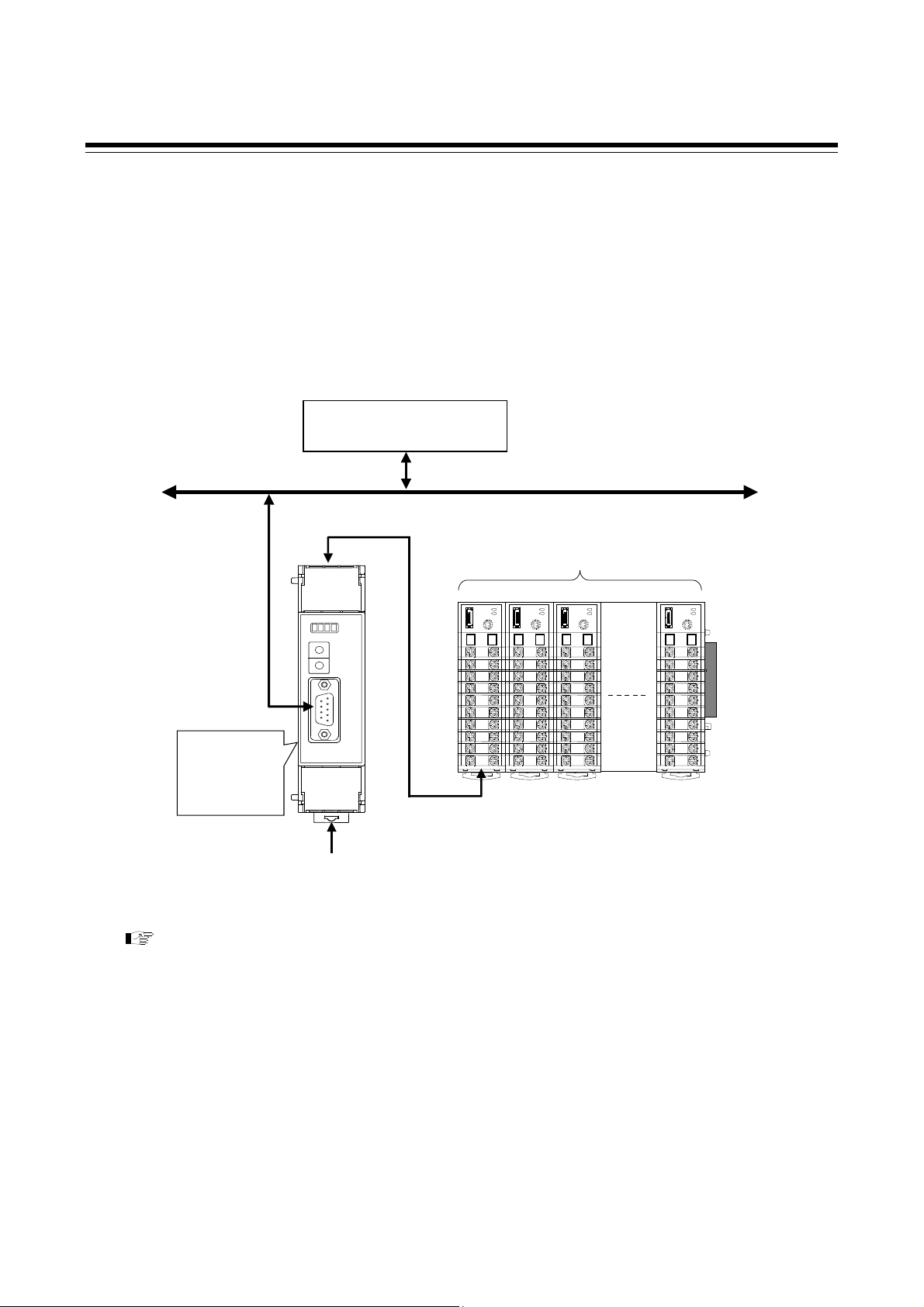
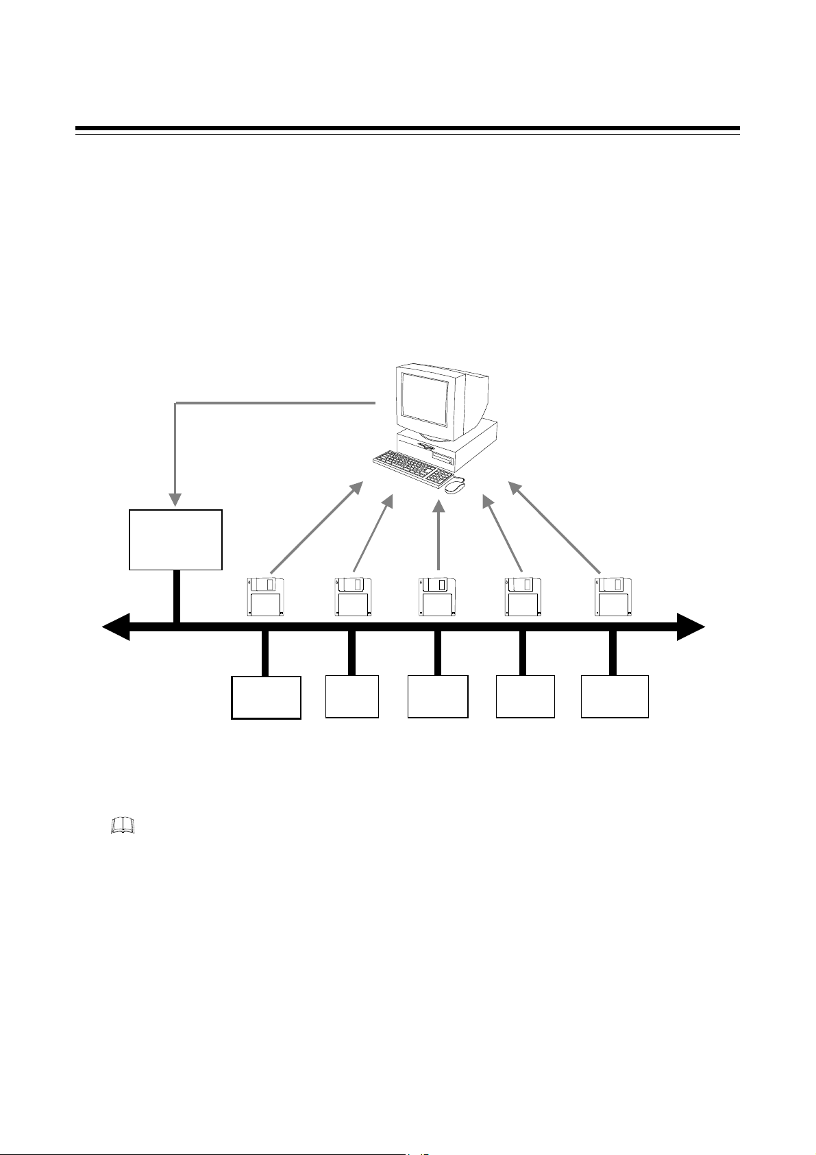
1. OUTLINE
This manual describes the communication specifications, mounting, wiring, setting and data
instructions for the PROFIBUS Communication Converter COM-JG [For SRZ].
PROFIBUS Communication Converter COM-JG [For SRZ] (hereafter called COM-JG) is
communication converter to connect the RKC module type controller SRZ to a programmable
controller (hereafter called PLC) for PROFIBUS.
The COM-JG supports PROFIBUS-DP protocol. This protocol includes master and slave. The PLC is
the master and the COM-JG is the slave.
Programmable controller
PLC (Master)
PROFIBUS-DP
SRZ unit
[Up to 31 modules]
PROFIBUS
communication
converter
COM-JG
(Slave)
Power supply (24 V DC)
(Z-TIO and Z-DIO module)
1 2 3 31
Controller communication
(RS-485: Modbus)
For PROFIBUS, refer to the website of PROFIBUS International.
URL: http://www.profibus.com/
IMR01Y35-E3 1
Page 8

1. OUTLINE
1.1 Product Check
Before using this product, check each of the following.
Model code
Check that there are no scratches or breakage in external appearance (case, front panel, terminal, etc).
Check that all of the accessories delivered are complete. (Refer to below)
COM-JG [For SRZ] Installation Manual
(IMR01Y23-E)
COM-JG [For SRZ] Quick Instruction Manual
(IMR01Y27-E)
COM-JG [For SRZ] Communication Data List
(IMR01Y31-E)
COM-JG [For SRZ] Instruction Manual
(IMR01Y35-E3)
Accessories Q’TY Remarks
1 Enclosed with instrument
1 Enclosed with instrument
1 Enclosed with instrument
This manual
1
(Download free or purchase hard copy)
GSD file * 1 Download free
If any of the products are missing, damaged, or if your manual is incomplete, please contact
RKC sales office or the agent.
* GSD file
The GSD file for COM-JG can be downloaded from the RKC official website.
(URL: http://www.rkcinst.com/english/download/field_network.htm)
1.2 Model Code
Check that the product received is correctly specified by referring to the following model code list:
If the product is not identical to the specifications, please contact RKC sales office or the agent.
COM- JG ∗ 02
Corresponding to the RKC controller
02: SRZ
2
IMR01Y35-E3
Page 9
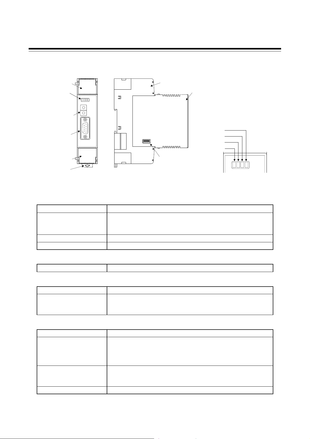
r
t
X
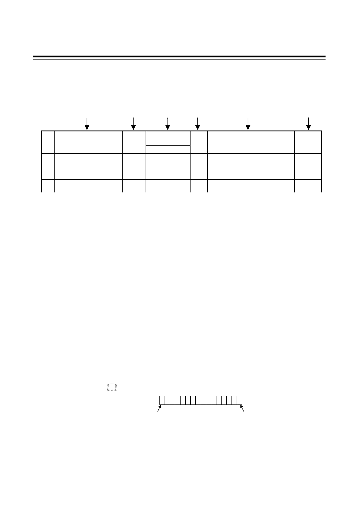
1.3 Parts Description
1. OUTLINE
Terminal cover
Indication
lamps
Address setting
switch
PROFIBUS
connector
(COM.PORT)
Terminal cove
Mounting
bracke
Front view
Indication lamps
FAIL [Red]
RUN [Green]
ONL [Green]
RX/TX [Green]
PROFIBUS connector
COM. PORT
Switches
Address setting switch
DIP switch
Others
Terminal cover
Mounting bracket
Terminal base
Mainframe
Terminal base
Mainframe
[Details of Indication lamps]
RX/T
ONL
RUN
FAIL
DIP switch
Left side view
• When instrument abnormally: Turns on
• When normally: Turns on
• Operation error: Flashes slowly
• During controller communication initialization: Flashes rapidly
During PROFIBUS connection establishment: Turns on
During PROFIBUS data send and receive: Flashes
Connector for PLC (Master) connection
Set the address for PROFIBUS
Set the communication speed for controller communication,
controller address auto obtain, and controller communication
enable/disable
Terminal covers above and below the COM-JG
• Used for the DIN rail mounting
• When panel mounted, two mounting brackets are required for the
upper and lower sides (one required for the upper side: separately
sold).
Part of the terminal and base of COM-JG
(There is the Termination resistor transfer switch in the inside of
terminal base)
Part of the mainframe of COM-JG
IMR01Y35-E3
3
Page 10

2. HANDLING PROCEDURES
Conduct the setting necessary for performing communication in accordance with the following procedure.
COM-JG Setting
Mounting
Wiring
and
Connection
Controller (SRZ) Setting
COM-JG Initial Setting
Communication Data
Setting
To avoid error at operation start-up, COM-JG must be powered on LAST (after the
controller, PLC, etc.).
Set the PROFIBUS address and DIP switch setting of COM-JG.
Refer to 5. SETTING (P. 15)
Install the COM-JG.
• Refer to 3. MOUNTING (P. 5)
• For controller (SRZ), refer to Z-TIO INSTRUCTION
MANUAL (IMS01T01-E) or Z-DIO
INSTRUCTION MANUAL (IMS01T03-E)
Connect power supply wires to the COM-JG, and also connect
the COM-JG to the controller (SRZ) and the COM-JG to the
PLC, respectively.
• Refer to 4. WIRING (P. 8)
• For controller (SRZ), refer to Z-TIO INSTRUCTION
MANUAL (IMS01T01-E) or Z-DIO
INSTRUCTION MANUAL (IMS01T03-E)
Set communication parameters of controller (SRZ).
• Refer to 8.3 Use Instruments Setting (P. 62)
• Refer to Z-TIO Host Communication Quick Manual
(IMS01T02-E) or Z-DIO INSTRUCTION
MANUAL (IMS01T03-E)
Set initial setting of the COM-JG.
• Refer to 5.3 COM-JG Initial Setting (P. 17)
• Refer to 5.4 Controller Address Auto Obtain
Methods
• Refer to 8.4 Contents Check of COM-JG Initial
Setting (P. 63)
• Refer to 8.5 PLC Tool Setting (P. 70)
Set PLC programming software STEP7.
Refer to 8.5 PLC Tool Setting (P. 70)
(P. 19)
4 IMR01Y35-E3
Page 11

3. MOUNTING
This chapter describes installation environment, mounting cautions, dimensions and mounting
procedures.
To prevent electric shock or instrument failure, always turn off the power before
mounting or removing the instrument.
WARNING
!
3.1 Mounting Cautions
(1) This instrument is intended to be used under the following environmental conditions. (IEC61010-1)
[OVERVOLTAGE CATEGORY II, POLLUTION DEGREE 2]
(2) Use this instrument within the following environment conditions:
• Allowable ambient temperature: −10 to +50 °C (14 to 122 °F)
• Allowable ambient humidity: 5 to 95 % RH
(Absolute humidity: MAX.W.C 29.3 g/m
• Installation environment conditions: Indoor use
Altitude up to 2000 m
(3) Avoid the following conditions when selecting the mounting location:
• Rapid changes in ambient temperature which may cause condensation.
• Corrosive or inflammable gases.
• Direct vibration or shock to the mainframe.
• Water, oil, chemicals, vapor or steam splashes.
• Excessive dust, salt or iron particles.
• Excessive induction noise, static electricity, magnetic fields or noise.
• Direct air flow from an air conditioner.
• Exposure to direct sunlight.
• Excessive heat accumulation.
(4) Mount this instrument in the panel considering the following conditions:
• Ensure at least 50 mm space on top and bottom of the instrument for maintenance and
environmental reasons.
• Do not mount this instrument directly above equipment that generates large amount of heat
(heaters, transformers, semi-conductor functional devices, large-wattage resistors).
• If the ambient temperature rises above 50 °C (122 °F), cool this instrument with a forced air fan,
cooler, etc. Cooled air should not blow directly on this instrument.
3
dry air at 101.3 kPa)
• In order to improve safety and the immunity to withstand noise, mount this instrument as far
away as possible from high voltage equipment, power lines, and rotating machinery.
High voltage equipment: Do not mount within the same panel.
Power lines: Separate at least 200 mm.
Rotating machinery: Separate as far as possible.
(5) If this instrument is permanently connected to equipment, it is important to include a switch or
circuit-breaker into the installation. This should be in close proximity to the equipment and within
easy reach of the operator. It should be marked as the disconnecting device for the equipment.
IMR01Y35-E3 5
Page 12

3. MOUNTING
t
3.2 Dimensions
109.5 3
6.5
30
(Unit: mm)
125
5
78
3.3 DIN Rail Mounting
Mounting procedures
1. Pull down the mounting bracket at the bottom of the instrument (A). Attach the hooks on the top
of the instrument to the DIN rail and push the lower section into place on the DIN rail (B).
2. Slide the mounting bracket up to secure the instrument to the DIN rail (C).
DIN rail
(B) Push
Mounting
bracke
6
(A) Pull down
(C) Locked
IMR01Y35-E3
Page 13

Removal procedures
1. Turn the power OFF.
2. Remove the wiring.
3. Pull down a mounting bracket with
a slotted screwdriver (A). Lift the
instrument from bottom, and take it
off (B).
3. MOUNTING
(B) Lift and take
off
(A) Pull down
3.4 Panel Mounting
Mounting procedures
1. Pull down the mounting bracket (A) until locked and that a mounting hole appears.
2. Prepare one mounting bracket per instrument (B) sold separately (KSRX-55) and then insert it in
the rear of the terminal board at top of the instrument until locked but a mounting hole does not
disappear.
3. Mount each module directly on the panel with screws which are inserted in the mounting holes of
the top and bottom mounting brackets.
Recommended tightening torque: 0.3 N⋅m (3 kgf⋅cm)
The customer needs to provide the M3 size screws. Select the screw length that matches the
mounting panel.
(B) Insert
Mounting dimensions
(Unit: mm)
IMR01Y35-E3
Mounting bracket
(Sold separately)
(KSRX-55)
(A) Pull down
Mounting
holes
M3
130.5 ± 0.2
7
Page 14

4. WIRING
This chapter describes wiring cautions, terminal configuration and connections.
4.1 Wiring Cautions
To prevent electric shock or instrument failure, do not turn on the power until all
wiring is completed. Make sure that the wiring is correct before applying power
to the instrument.
• To avoid noise induction, keep communication signal wire away from instrument power line, load
lines and power lines of other electric equipment.
• If there is electrical noise in the vicinity of the instrument that could affect operation, use a noise
filter.
− Shorten the distance between the twisted power supply wire pitches to achieve the most effective
noise reduction.
WARNING
!
− Always install the noise filter on a grounded panel. Minimize the wiring distance between the
noise filter output and the instrument power supply terminals to achieve the most effective noise
reduction.
− Do not connect fuses or switches to the noise filter output wiring as this will reduce the
effectiveness of the noise filter.
• Power supply wiring must be twisted and have a low voltage drop.
• For an instrument with 24 V power supply, supply power from a SELV circuit.
• A suitable power supply should be considered in end-use equipment. The power supply must be in
compliance with a limited-energy circuits (maximum available current of 8 A).
• Use the solderless terminal appropriate to the screw size (M3).
• Make sure that the any wiring such as solderless terminal is not in contact with the adjoining terminals.
5.9 mm or less
3.2 mm or more
Recommended tightening torque:
0.4 N⋅m (4 kgf⋅cm)
8 IMR01Y35-E3
Page 15
4.2 Terminal Configuration
The terminal layout is as follows.
Upper-side
terminal
3
7 6 5 4
2 1
Controller
communication
RS-485
T/R(A)
1
T/R(B)
5
SG
4
4. WIRING
: The part of internal wiring
Power supply
11 10 9 8
Ground
14 13 12
9
8
12
DC
−
+
24 V
Lower-side
terminal
FG
As controller communication terminal Nos. 1, 4 and 5 are internally connected to terminal Nos. 3,
6 and 7, any terminals can be used.
As ground and power supply terminal Nos. 8, 9 and 12 are internally connected to terminal Nos.
10, 11 and 14, any terminals can be used.
Terminal No. 2 and No. 13 is not used.
IMR01Y35-E3
9
Page 16
4. WIRING
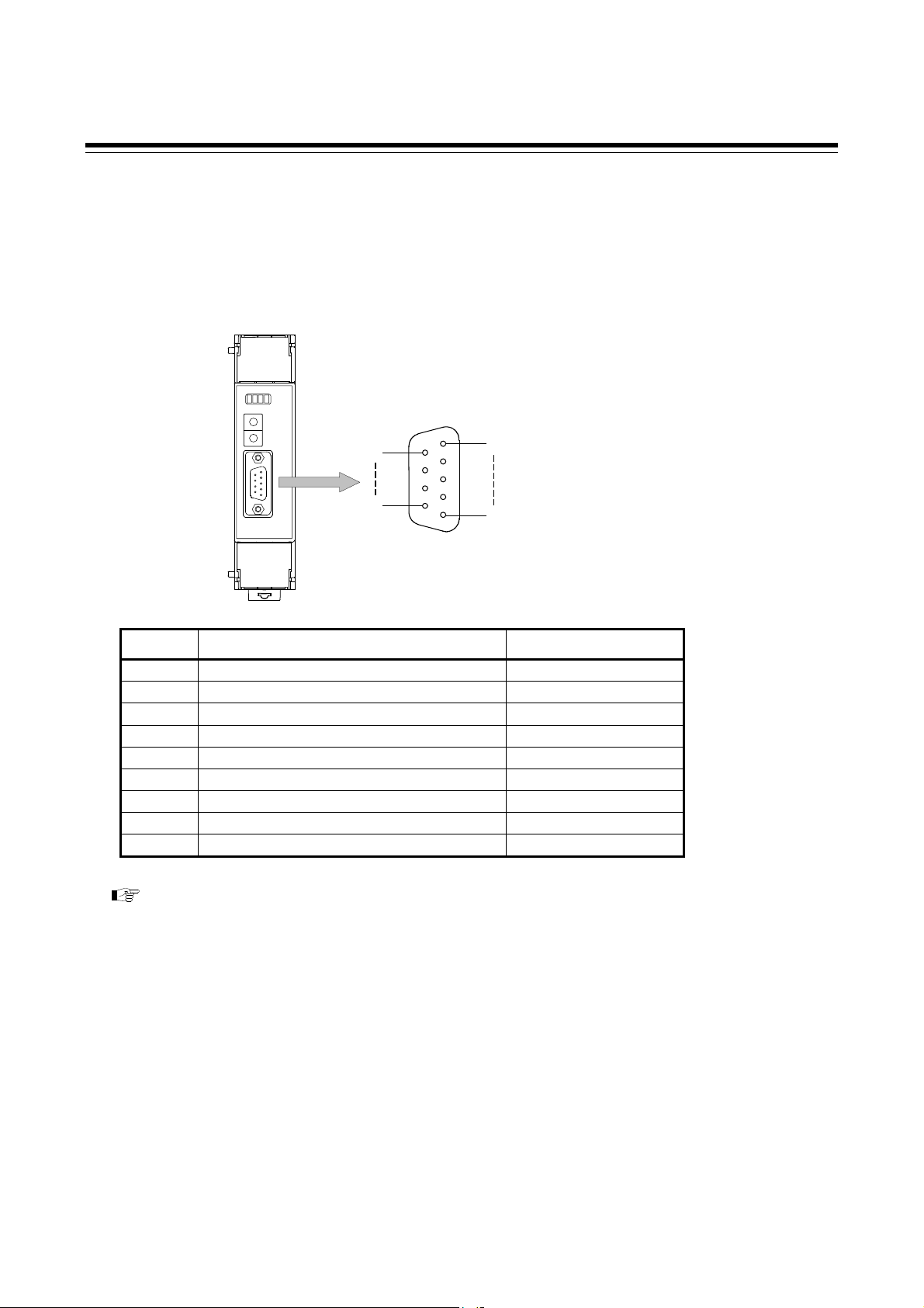
4.3 Connection to PROFIBUS
Connect COM-JG to PROFIBUS.
Pin layout of connector
COM-JG
PROFIBUS connector
(COM. PORT)
9
6
5
1
Pin No. Signal name Symbol
1
2
⎯
⎯
Unused
Unused
3 Receive data /Transmission data (plus) RxD/TxD-P
4
⎯
Unused
5 Signal ground DGND
6 Termination resistor supply voltage (5 V) VP
7
⎯
Unused
8 Receive data /Transmission data (negative) RxD/TxD-N
9
⎯
Unused
For the connectable connector of the PLC, refer to the instruction manual for the used PLC.
10
IMR01Y35-E3
Page 17

Ω
Ω
Ω
PROFIBUS cables
Use the PROFIBUS cable which fitted the following requirement.
• Use the shielded twisted pair wire
• Based on IEC61158, Standard (Recommend cable type A)
Cable type A specification
Impedance: 135 to 165 Ω
Capacitance: < 30 pF/m
Loop resistance: 110 Ω/km
Core diameter: 0.64 mm
Core cross section: > 0.34 mm
Maximum cable length by communication speed (For cable type A)
Communication speed (kbps)
Cable length (m)
2
9.6 19.2 93.75 187.5 500 1500 12000
1200 1200 1200 1000 400 200 100
4. WIRING
• Connect the termination resistor to the end of a bus (Refer to below)
Signal
RxD/TxD-P
RxD/TxD-N
DGND
VP
Termination resist or
390
220
390
Customer must provide the PROFIBUS cable (a connection cable of PLC and COM-JG).
As for the PROFIBUS cable, there is a case prepared by a PLC manufacturer.
The details except the above are connected to a website of PROFIBUS International, and
obtain necessary information.
URL: http://www.profibus.com/
IMR01Y35-E3
11
Page 18
4. WIRING
4.4 Connection to the Controllers
Conduct wiring between the COM-JG and controller (SRZ) as shown in the following.
SRZ (Z-TIO module/Z-DIO module) communication terminal number and
signal details
Terminal No. Signal name Symbol
3 Send/Receive data T/R (A)
4 Send/Receive data T/R (B)
5 Signal ground SG
Wiring
COM-JG
(−)
T/R (A)
RS-485
1
Paired
wire
Communication
terminal No.
Controller (SRZ)
Z-TIO module
3
T/R (A)
SRZ base section
2 1
3 4 5
(−)
(+)
R1: Internal termination resistor
(Example: 120 Ω 1/2 W)
R2: Termination resistor for external
connection (120 Ω 1/2 W)
T/R (B)
R1
Terminal block
Shielded twisted
5
SG
4
pair wire
For termination resistors, refer to
Connected by
the internal
communication
line
R2
4
T/R (B)
5
SG
Z-TIO module
3
T/R (A)
4
T/R (B)
5
SG
(+)
(−)
(+)
4.5 Installation of Termination
Resistor (P. 13)
Up to 16 Z-TIO modules can be connected.
The cable and termination resistor(s) must be provided by the customer.
A combined total of up to 31 Z-TIO and Z-DIO modules can be connected in the SRZ,
however, in some cases this may not be possible due to restrictions related to the number of
connected channels and communication items.
[ Refer to 6.2.1 Data type and data length of communication data (P. 22)]
12
IMR01Y35-E3
Page 19

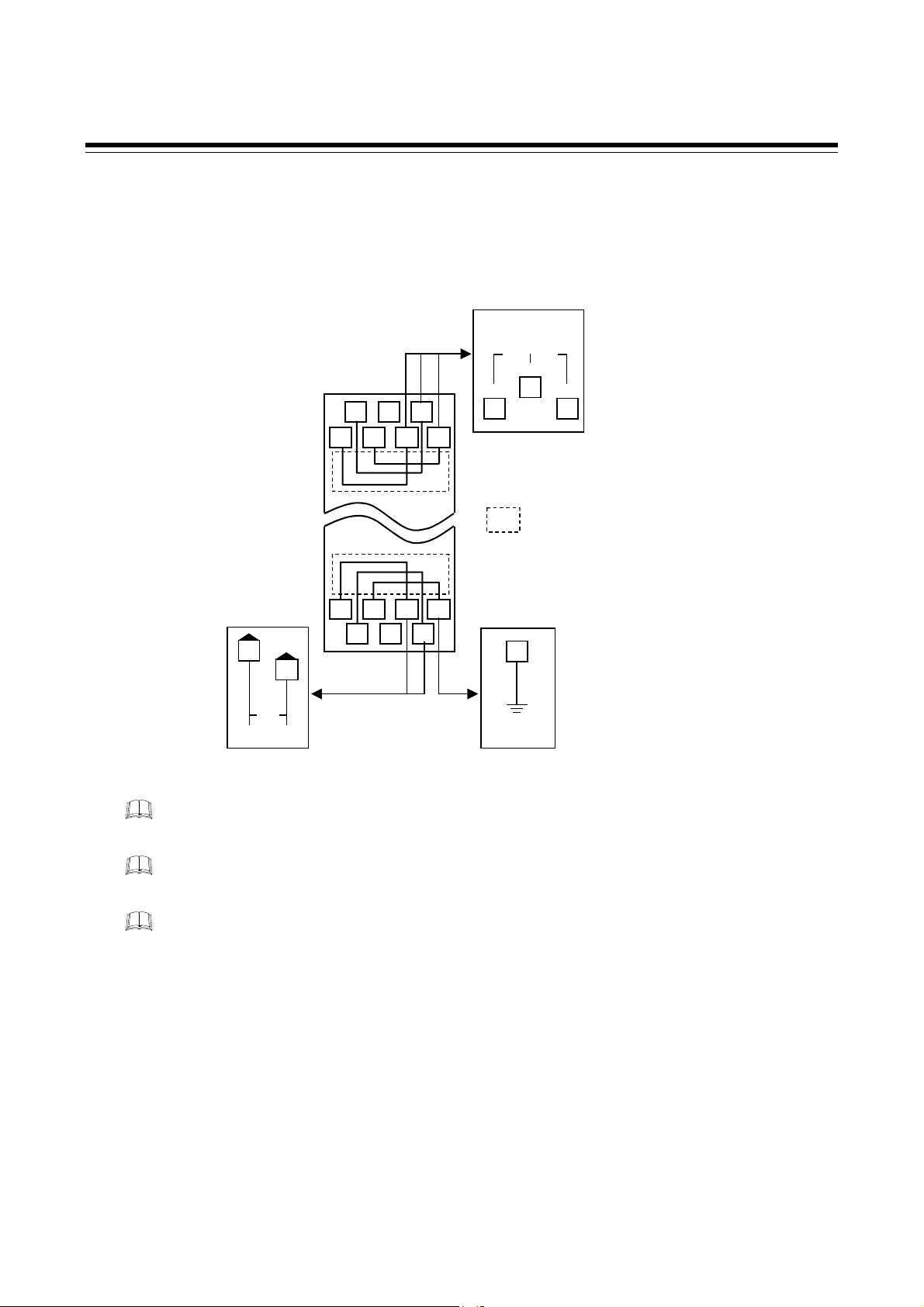
4. WIRING
r
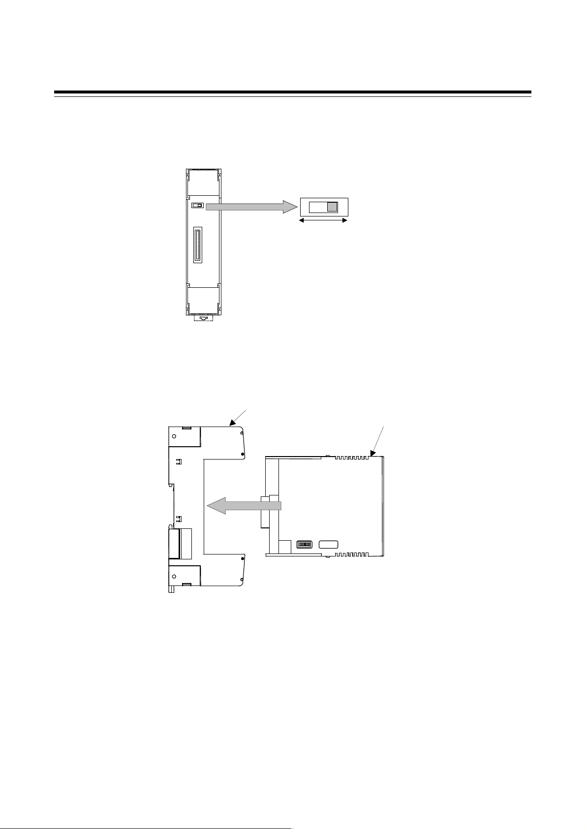
4.5 Installation of Termination Resistor
Procedure for setting a termination resistor to Controller communication (RS-485) and its setting
position are described in the following.
If communication errors occur frequently due to the operation environment or the
communication distance, connect termination resistors.
Termination resistor setting position
If the COM-JG is connected to the extreme end of the communication line, install one termination
resistor each to the COM-JG and the controller (module of the SRZ) located most distantly from the
COM-JG.
Termination
resistor ON
(Factory
set value)
COM-JG
Z-TIO or Z-DIO module
Internal communication line
Controller communication
(RS-485: Modbus)
Setting procedure of termination resistor (COM-JG)
SRZ unit
Connect a termination
resistor to the terminals
from exterior.
(RS-485)
Termination resisto
As the COM-JG is internally provided with a selector switch for choosing the ON/OFF of a
termination resistor, it is not required to externally install the termination resistor.
(Factory set value: Termination resistor connected)
1. Turn off the power supply of the COM-JG.
Do not separate the mainframe from terminal base with the power turned on. If so,
instrument failure may result.
2. Pull out the mainframe itself toward you while pushing the locks at its top and bottom (1), and
then separate it from the terminal base (2).
Upper-side
lock
Lower-side
lock
Top view
Bottom view
Terminal base
Removing the module mainframe
Mainframe
(1) Push
(2) Pull out
(1) Push
IMR01Y35-E3
13
Page 20
4. WIRING
3. Turn on the Termination resistor transfer switch in the terminal base.
The COM-JG is shipped from the factory with the selector switch set to “ON: Termination
resistor connected.”
Termination resistor
transfer switch
ON
OFF
Termination
resistor
OFF
Termination
resistor
ON
(120 Ω 1/2 W)
Factory set value
: ON
A terminal base of the state which removed module mainframe
4. Push the mainframe thus separated in the terminal base until firmly locked.
Terminal base
Mainframe
Push the module
mainframe until
firmly locked
14
Mounting the module mainframe
IMR01Y35-E3
Page 21
5. SETTING
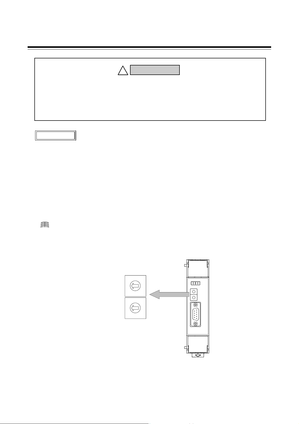
WARNING
!
To prevent electric shock or instrument failure, always turn off the power
before setting the switch.
To prevent electric shock or instrument failure, never touch any section other
than those instructed in this manual.
CAUTION
Do not separate the mainframe from the terminal base with the power turned on.
If so, instrument failure may result.
5.1 PROFIBUS Address Setting
The master communicates with the selected slave by specifying that slave’s address number. Each
slave must have a unique address number for this data transmission. Set the slave address with the
address setting switch prior to operation.
With the tow rotary switch in the front of the COM-JG, set an address number on the PROFIBUS. For
this setting, use a small slotted screwdriver.
No communication with PROFIBUS can be conducted with each factory set value (00h)
left as it is. Set it to the same value as the PROFIBUS address set when system
configured.
High-order digit
setting
(Set value × 10h)
Low-order digit
setting
(Set value × 1h)
Address setting switch
4
5
6
3
7
2
8
1
9
0
A
F
B
E
D
C
4
5
6
3
7
2
8
1
9
0
A
F
B
E
D
C
COM-JG
Setting range:
1 to 125 [01h to 7Dh: hexadecimal]
(Factory set value: 00h)
IMR01Y35-E3 15
Page 22

5. SETTING
5.2 DIP Switch Setting
Configure settings for controller communication speed, controller address auto obtain, and controller
communication enable/disable using the DIP switches on the left side of the mainframe.
DIP switch
ON
12345678
12345678
ON
OFF
Left side view
1 2 Controller communication speed
OFF OFF 38400 bps
ON OFF 9600 bps
OFF ON 19200 bps
ON ON 38400 bps
Factory set value: 19200 bps
4 Controller address auto obtain
OFF
ON
Factory set value: Auto obtain off
(No controller address search when power is turned on)
(Controller address search and update when power is turned on)
Refer to 5.4 Controller Address Auto Obtain Methods (P. 19).
Auto obtain off
Auto obtain on
7 Controller communication enabled/disabled
OFF
ON
(When COM-JG initial settings are configured using PLC tool)
Controller communication enabled
Controller communication disabled
16
Factory set value: Controller communication enabled
Refer to 5.3 COM-JG Initial Setting (P. 17).
3 5 6 8
OFF OFF OFF OFF
(Do not change the factory set value)
Fixed
Dip switch No. 3, 5, 6 and 8 must be always OFF. Do not set to ON.
IMR01Y35-E3
Page 23

5. SETTING
5.3 COM-JG Initial Setting
To perform communication between a PLC and controller (SRZ), the following items must be set to
COM-JG. These settings are configured using the configuration tool of the PLC.
Preparations and an overview of the settings are explained below.
[COM-JG initial setting items]
• Controller address
• Number of continuous accesses
• Continuous accesses enable selection
• Static data read/write range
• Transmission wait time of controller communication
For the concrete setting method of using the PLC configuration tool, refer to 8.5 PLC Tool
Setting (P. 70).
Setting preparations
To configure the COM-JG initial setting items, controller communication must be disabled using the
DIP switches.
Change DIP switch No. 7 to ON (controller communication disabled) on the left side of the COM-JG.
DIP switch
ON
1234567 8
1234567 8
ON
OFF
ON: Controller communication
disabled
When you have completed the initial settings of the COM-JG, be sure to return DIP switch
No. 7 to OFF (controller communication enabled).
Setting overview
• Controller address (required setting)
This is required in order to make the COM-JG recognize the address of each controller (SRZ
module). Controller addresses can be obtained automatically by switching DIP switch No. 4.
For controller address auto obtain, refer to 5.4 Controller Address Auto Obtain
Methods (P. 19).
IMR01Y35-E3
17
Page 24

5. SETTING
• Number of continuous accesses (elective setting)
Each module in the controller (SRZ) has multiple channels, and thus in the case of a 4-channel
type Z-TIO module, four data areas (data parameters) must be retained for each communication
item. However, the number of continuous accesses setting can be configured to allow
communication with just one data area (data parameter) per communication item regardless of the
number of channel.
In a static data request, a combined total of up to 40 read and write items can be
communicated.
The factory set value for the number of continuous accesses is “4,” and thus when the
controller (SRZ) configuration consists only of 4-channel type Z-TIO modules, the
setting does not need to be configured.
For information on the number of continuous accesses, refer to also Number of
continuous accesses (P. 65) in 8.4 Contents Check of COM-JG Initial Setting.
• Continuous accesses enable selection (elective setting)
When the communication items of a static data request contain both channel-based data and
module-based data, the number of continuous accesses setting must be disabled for module-based
.
data
When only channel-based data is communicated, this setting is not necessary.
For information on the continuous accesses enable selection, refer to also Continuous
accesses enable selection (P. 66) in 8.4 Contents Check of COM-JG Initial Setting.
• Static data read range (elective setting)
When a communication item is specified in a static data request, a read or write request is
normally sent to the same Modbus register address of all connected controllers (each module of
the SRZ).
For example, when a Z-TIO module and a Z-DIO module of an SRZ are connected and a
communication item of the Z-TIO module is read, the data of the same Modbus register address
in the Z-DIO module as the communication item specified in the Z-TIO module is read. However,
because the contents of the Modbus register addresses of the Z-TIO module and the Z-DIO
module are different, different data is read from each.
To avoid having unnecessary data read, the range of data that can be communicated for the same
module type can be assigned.
This setting is not necessary when the controller consists only of modules that are the
same type.
For information on the static data read range, refer to also Static data read/write
range (P. 68) in 8.4 Contents Check of COM-JG Initial Setting.
• Static data write range (elective setting)
Same as the static data read range.
• Transmission wait time of controller communication (elective setting)
This setting is normally not necessary.
18
IMR01Y35-E3
Page 25

5. SETTING
5.4 Controller Address Auto Obtain Methods
To allow the PLC and COM-JG to communicate, the COM-JG must be made to recognize the address
of each controller (the module addresses of the SRZ).
Although the PLC configuration tool can be used to configure settings to make the COM-G recognize
the controller addresses, the DIP switches can be set to have the settings configured automatically.
For setting method using the PLC configuration tool, refer to 5.3 COM-JG Initial Setting (P. 17),
8.4 Contents Check of COM-JG Initial Setting (P. 63) and 8.5 PLC Tool Setting (P. 70).
Procedure
This procedure assumes that the controller (SRZ) communication settings have been
completed.
To execute controller address auto obtain, DIP switch No. 7 on the left side of the COM-JG
must be set to OFF (controller communication enabled).
1. Set DIP switch No. 4 on the left side of the COM-JG to ON (auto obtain ON).
Set the controller communication speed with DIP switch Nos. 1 and 2.
Set the controller communication speed to the same value as the controller (SRZ) setting.
For the DIP switch setting, refer to 5.2 DIP Switch Setting (P. 16).
DIP switch
ON
12345678
12345678
ON
OFF
ON: Auto obtain ON
Controller communication
speed setting
(19200 bps)
2. Connect the power wiring and the wiring between the COM-JG and the controllers (SRZ).
There is no need for the COM-JG to be connected to the PROFIBUS when controller
address auto obtain is executed.
IMR01Y35-E3
19
Page 26

5. SETTING
3. When the power is turned on, controller address auto obtain starts.
While auto obtain is in progress, the RUN lamp of the COM-JG blinks.
The obtained addresses are stored in “Controller address” in the COM-JG initial setting items.
“Controller address” has 31 address spaces, Nos. 1 to 31 [equal to the maximum number of
controller (SRZ) connections], and the obtained addresses are stored in order from No. 1
beginning from the lowest-value address.
The COM-JG checks each controller (SRZ) address against addresses 1 to 99. For this
reason, a certain amount of time is required to complete auto obtain (up to about 90
seconds).
4. When controller address auto obtain is finished, the RUN lamp of the COM-JG stops blinking
and lights steadily.
5. Turn off the power and return DIP switch No. 4 on the left side of the COM-JG to OFF (auto
obtain OFF).
[Example] When the controller (SRZ) configuration is three Z-TIO modules and two Z-DIO modules
Obtained address
Z-TIO
module
Z-DIO
module
COM-JG
1 5 10 17 30
SRZ
Controller address
(Module address)
COM-JG initial setting item
No. 1 Controller address 1
No. 2 Controller address 5
No. 3 Controller address 10
No. 4 Controller address 17
No. 5 Controller address 30
No. 6 Controller address 0
No. 31 Controller address 0
Automatically obtained
controller addresses
Addresses are stored in
order from No. 1 from the
lowest address.
In this example there are
five modules, and thus the
automatically obtained
addresses are stored in Nos.
1 to 5.
The data in controller addresses 6 to 31 will be “0” (No controller connected).
20
The controller address of a Z-TIO module will be the value (decimal) set in the address
setting switch plus “1.” The controller address of a Z-DIO module will be the value
(decimal) set in the address setting switch plus “17.”
IMR01Y35-E3
Page 27
6. PROFIBUS COMMUNICATION
6.1 PROFIBUS System Configuration
For system configuration with PROFIBUS-DP protocol, have to offer the communication information
about each slave for a master in the form of electronic device data seat (GSD file).
A manufacturer of PLC (master) has prepared configuration tool for a system configuration of
PROFIBUS. By combining all GSD files of the slaves to be connected, the configuration tool creates a
master parameter record containing all pertinent data for the bus system. The configuration of a
PROFIBUS system is enabled by downloading these data to a master.
System configuration
PROFIBUS
configuration tool
PLC
(Master)
GSD file
PROFIBUS-DP
COM-JG
Overview of PROFIBUS system configuration
I/O
Sensor Drive
Slave
Field
device
About configuration tool, please ask a manufacturer of a master product.
IMR01Y35-E3 21
Page 28

6. PROFIBUS COMMUNICATION
6.2 PROFIBUS Communication Data
6.2.1 Data types and data length of communication data
Data access types
• Static data read/write
• Dynamic data read/write
• Error state register
• Write permission flag register
• Write control flag register
Communication data length
A maximum of 170 bytes can be read or written.
Static data request
The maximum number of communication items which can be specified:
40 items (Read items+Write items)
The communication items which can be specified:
Data of the 7. COMMUNICATION DATA MAP (P. 28)
Dynamic data request
The communication items which can be requested:
Data of the 7. COMMUNICATION DATA MAP (P. 28)
The number of communication items becomes as follows depending on the number of
connection channels.
[Read data] Number of static read data × Number of connection channel
Number of dynamic data × 6 + 12
[Write data] Number of static write data × Number of connection channel
Number of dynamic data × 6 + 11
a
Total number of continuous accesses
b
(Error state register: 1 byte)+(Write permission flag register: 1 byte)+(Write control flag register: 10 bytes) = 12
c
(Write permission flag register: 1 byte)+(Write control flag register: 10 bytes) = 11
b
≤ 170
c
≤ 170
Number of connection channels Number of static data *
1 channel Maximum of 40 items for both read and write.
16 channels Maximum of 5 items for both read and write.
31 channels Maximum of 2 items for both read and write.
* Calculated with the number of dynamic data equal to 0. The 10 bytes of the write control flag register
for read data and the 10 bytes of the write control flag register for write data can be omitted.
6.2.2 Static data request
a
× 2 +
a
× 2 +
• Static data is that which is always read/written from/to the PROFIBUS master such as the PLC. The
data item is selected by the configuration tool such as the PLC.
• As the Modbus register address is directly specified, data items of all the controllers connected to the
COM-JG can be selected.
• When static data is requested, 1-word (2-byte) data is used for both read and write.
As the static data register address is set when system configured, it is not required to create a
sequence program for static data assignment.
22
IMR01Y35-E3
Page 29

6. PROFIBUS COMMUNICATION
6.2.3 Dynamic data request
• Dynamic data is that which is freely read/written from/to the PROFIBUS master such as the PLC.
The data item is freely selected by the sequence program.
• As the Modbus register address is directly specified, data items of all the controllers connected to the
COM-JG can be selected.
• When dynamic data is requested, 3-word (6-byte) data is used for both read and write.
Send data from PLC to COM-JG
Register configuration
Byte 0 Byte 1 Byte 2 Byte 3 Byte 4 Byte 5
Attribute
Device
address
Communication item
address
Byte 0: Specify an attribute of data. Only Bit 7 and Bit 6 are used.
Byte 0 (Attribute)
Communication item
data
Bit 7 Bit 6
Bit 0
Bit 6: Send data validate/invalidated discriminating bit
0: Send data is validated
1: Send data is invalidated
Bit 7: Read/Write discriminating bit
0: Data read
1: Data write
Unused (Any value, even if set, is ignored.)
Byte 1: Specify an accessing device address of controller.
Data range: 1 to 99 (“0” at Modbus is invalidated)
Byte 2, Byte 3: The communication item address of controller, to/from which data
is written/read is specified.
Z-TIO module Data address range: 0000H to 035BH
Z-TIO module Address range of memory area: 0500H to 0553H
Z-DIO module Data address range: 0000H to 00DBH
Byte 4, Byte 5: Write data of a communication item.
− If Bit 7 in Byte 0 is set to “1: Data write,” data in the address specified by
Bytes 1, 2, and 3 is written.
− If Bit 7 in Byte 0 is set to “0: Data read,” data in Byte 4 and 5 will be
ignored.
For communication item, refer to 7. COMMUNICATION DATA MAP (P. 28).
IMR01Y35-E3
23
Page 30

6. PROFIBUS COMMUNICATION
PLC received data from COM-JG
Register configuration
Byte 0 Byte 1 Byte 2 Byte 3 Byte 4 Byte 5
Attribute
Byte 0: Echo back of Byte 0 of send data, and data updating state of
controller (Bit 5)
Device
address
Communication item
address
Communication item
data
The details of data in Byte 0 sent to the controller from the PLC and data
updating state of controller (Bit 5) are returned.
Byte 0 (Attribute)
Bit 7 Bit 6 Bit 5
Bit 0
Bit 6: Send data validate/invalidate discriminating bit
0: Send data is validated
1: Send data is invalidated
Bit 7: Read/Write discriminating bit
0: Data read
1: Data write
Unused (Any value, even if set, is ignored.)
Bit 5: Data updating state of controller
0: Data update
1: Data non-update
Byte 1: Echo back of Byte 1 of send data
The specified controller device address is returned. However, if there is no
specified device address, “FFH” is returned.
Byte 2, Byte 3: Echo back of Byte 2 and Byte 3 of send data
The communication item address of controller, to/from which data is
written/read is returned. However, if any communication item address out of the
data range or of unused item is specified, “FFFFH” is returned.
Z-TIO module Data address range: 0000H to 035BH
Z-TIO module Address range of memory area: 0500H to 0553H
Z-DIO module Data address range: 0000H to 00DBH
Byte 4, Byte 5: Data of communication item
− For data read, the current value of relevant communication item is stored.
− For data write, the current value of relevant communication item is stored.
If the written data is validated, the written value is returned.
If the written data is invalidated, the present (before data write) value is
returned.
When the data is written, there is a delay in rewriting the data in this
register as the COM-JG updates the register after rereading the data on
the controller.
24
IMR01Y35-E3
Page 31

6. PROFIBUS COMMUNICATION
6.2.4 Registers assigned to PLC
Set the register area after the GSD file is read to the configuration tool for the PLC.
The static data request read, static data request write and dynamic data request registers are set to the
register area.
In addition to the above register area setting, the following data is set at the beginning of the register.
• Read register: Error state (1-byte), Write permission flag (1-byte), Write control flag (10-byte)
• Write register: Write permission flag (1-byte), Write control flag (10-byte)
Error state register
The first read only 1-byte register consists of bits of error state.
Error state register
Bit 7 Bit 3 Bit 2 Bit 1 Bit 0
Unused
Bit 0: Instrument error
0: No instrument error
1: Instrument error
Bit 1: Time-out error
0: No time-out error
1: Time-out error
Bit 2: Controller communication validate/invalidate
0: Controller communication is validated
1: Controller communication is invalidated
Bit 3: Controller communication initialization
0: Completed initialization of controller communication
1: During initialization of controller communication
Instrument error
In case of the following either, become an error.
− None of the controllers is connected.
− COM-JG is hardware abnormally.
If an instrument error occurs, the RUN lamp at the front of COM-JG flashes (flashes slowly).
Time-out error
Successive communication time-out occurring twice in the same controller after PROFIBUS is
initialized causes a time-out error. Communication continues even during the time-out error and
recovers with no time-out error when the communication returns to normal.
Time-out time: 3 seconds
IMR01Y35-E3
25
Page 32

6. PROFIBUS COMMUNICATION
Controller communication validate/invalidate
Interlocked with dip switch No. 7 at the side of the COM-JG.
Factory set value of dip switch No. 7: OFF (0: Controller communication validate)
Controller communication initialization
Indicates the controller communication initialized state when the power is turned on and at this state
invalidates the data on each communication item.
Write permission flag register
Data may be written by static data request depending on the PLC even if the PLC is not in the RUN
state. In order to prevent this, the COM-JG is provided with the 1-byte flag register.
Only when the flag value in this one byte corresponds to “0FH” (hexadecimal), data is written to each
controller.
The operation of writing a hexadecimal value of “0FH” to the write permission flag
register is necessary for both static and dynamic data requests.
Write control flag register
This register controls whether data writing is “permitted” or “not permitted” for each requested word.
Permitted or not permitted is set by bit for each requested word of a static data write request.
0: Not permitted
1: Permitted
The write control flag register allocates a static data write request for 10 bytes of data with each byte
containing 8 words, and sets the bit for each word to “permitted” or “not permitted.”
[Example] Write “permitted” or “not permitted” state when the value of the first byte of the write
control flag register is A5H (hexadecimal)
A5H (hexadecimal) = 10100101 (binary)
1st byte 2nd byte 3rd byte 4th byte 5th byte 6th byte 7th byte 8th byte 9th byte 10th byte
1 to 8
words
9 to 16
words
17 to 24
words
25 to 32
words
33 to 40
words
41 to 48
words
49 to 56
words
57 to 64
words
65 to 72
words
73 to 80
words
8th word 7th word 6th word 5th word 4th word 3rd word 2nd word 1st word
1 0 1 0 0 1 0 1
The write control flag register is only effective for writing of static data requests.
26
If you do not need to set write “permitted” or “not permitted” for each word, this setting can
be omitted.
IMR01Y35-E3
Page 33

6. PROFIBUS COMMUNICATION
6.3 Processing of Numeric Data Values
Numeric data values used via communication with the PLC and processed by COM-JG include those
with and without decimal points and also those with minus signs.
For numeric data value without decimal point
If there is no decimal point, the value is processed as it is.
In parameters which only have ON or OFF status, 1 = ON, 0 = OFF.
[Example]
A signal wire for temperature input is disconnected and the burnout state occurs.
→ Read value corresponding to communication item address 0021 (Burnout state monitor):
1 (Hexadecimal number: 0001H)
For numeric data value with decimal point
The decimal point is omitted.
[Example 1]
When temperature measured value of controller is 120.5 °C
→ Read value corresponding to communication item address 0000 [Measured value (PV)]:
1205 (Hexadecimal number: 04B5H)
[Example 2]
When temperature measured value of controller is 130 °C
→ Read value corresponding to communication item address 0000 [Measured value (PV)]:
130 (Hexadecimal number: 0082H)
For numeric data value with minus sign
The value is expressed as a 2’s complement value which is obtained by subtracting the minus value
from the hexadecimal number 10000H.
[Example 1]
When temperature measured value of controller is −1 °C
→ Read value corresponding to communication item address 0000 [Measured value (PV)]:
Hexadecimal number: FFFFH
(10000H − 1 = FFFFH)
[Example 2]
When temperature measured value of controller is −2.5 °C
→ Read value corresponding to communication item address 0000 [Measured value (PV)]:
Hexadecimal number: FFE7H
(10000H − 25 = 10000H − 19H = FFE7H)
The original minus value can be found by revising the WORD value to the INT value on the
sequence program side.
IMR01Y35-E3
27
Page 34
7. COMMUNICATION DATA MAP
7.1 Reference to Communication Data Map
A data map of communication items shows data on controller (SRZ) which can make communication
via PROFIBUS.
(1)
(2)
No. Name Channel
1 Measured value (PV)
2 Comprehensive event state
CH1
CH2
CH3
CH4
CH1 0004 4
(3)
Modbus
register address
HEX DEC
0000
0001
0002
0003
0
1
2
3
(4)
Attri-
bute
RO Input scale low to Input scale high
RO Bit data
(5)
Data range
(6)
Factory
set value
⎯
⎯
(1) Name: Communication item name
(2) Channel: Channel numbers of each function module (Z-TIO, Z-DIO)
(3) Modbus register address:
The communication item address is the address number to specify with
configuration tool when carry out read/write of data.
HEX: Hexadecimal
DEC: Decimal
With respect to the following communication data of the Z-TIO module, the
register addresses of the indicated channels are non-used areas.
• 2-channel type module: Register addresses of the 3rd and 4th channels
• Heat/Cool control and Position proportioning control:
Register addresses of the 2nd and 4th channels *
• Cool-only communication data of Heat/Cool control:
Register addresses of the 2nd and 4th channels *
* Communication data with a ♣ mark in the name column
(4) Attribute: RO: Read only data
Data direction: Master (PLC) → Slave (COM-JG)
R/W: Read and Write data
Data direction: Master (PLC) ↔ Slave (COM-JG)
(5) Data range: Read or write range of communication data
Bit image of bit data is as follows.
16-bit data
…………….……………………
Bit 15
Bit 0
(6) Factory set value: Factory set value of communication data
28 IMR01Y35-E3
Page 35

7. COMMUNICATION DATA MAP
Communication includes both Normal setting data and Engineering setting data.
During RUN (control), the attribute of Engineering setting data is RO. To configure
Engineering setting data, the RUN/STOP switch must be set to STOP (control stopped).
Z-TIO module: Normal setting data No. 1 to 83,
Engineering setting data No. 85 to 207
Z-DIO module: Normal setting data No. 1 to 13,
Engineering setting data No. 15 to 28
The Engineering setting data should be set according to the application before setting any
parameter related to operation. Once the Engineering setting data are set correctly, no
further changes need to be made to datas for the same application under normal conditions.
If they are changed unnecessarily, it may result in malfunction or failure of the instrument.
RKC will not bear any responsibility for malfunction or failure as a result of improper changes
in the Engineering setting.
IMR01Y35-E3 29
Page 36

7. COMMUNICATION DATA MAP
7.2 Communication Data of Z-TIO Module
Modbus
CH2
CH3
CH4
CH1
CH2
CH3
CH4
CH1
CH2
CH3
CH4
CH1
CH2
CH3
CH4
CH1
CH3
CH1
CH2
CH3
CH4
CH2
CH3
CH4
register address
HEX DEC
0000
0001
0002
0003
0004
0005
0006
0007
0008
0009
000A
000B
000D
000E
000F
0010
0011
Unused
0012
Unused
0015
0016
0017
0018
0019
001A
001B
001C
No. Name Channel
1 Measured value (PV) CH1
2 Comprehensive event
state
3 Operation mode state
monitor
4 Error code ⎯ 000C 12 RO Bit data
5 Manipulated output value
(MV) monitor [heat-side]
♣
6 Manipulated output value
(MV) monitor [cool-side]
♣
7 Current transformer (CT)
input value monitor
8 Set value (SV) monitor CH1
Unused
Unused
0
1
2
3
4
5
6
7
8
9
10
11
13
14
15
16
17
Unused
19
Unused
21
22
23
24
25
26
27
28
Attri-
bute
RO Input scale low to Input scale high ⎯
RO Bit data
Bit 0: Event 1 state
Bit 1: Event 2 state
Bit 2: Event 3 state
Bit 3: Event 4 state
Bit 4: Heater break alarm state
Bit 5: Temperature rise completion
Bit 6: Burnout
Bit 7 to Bit 15: Unused
Data 0: OFF 1: ON
[Decimal number: 0 to 127]
RO Bit data
Bit 0: Control STOP
Bit 1: Control RUN
Bit 2: Manual mode *
Bit 3: Remote mode *
Bit 4 to Bit 15: Unused
Data 0: OFF 1: ON
[Decimal number: 0 to 15]
* During operation in manual mode, the manual
mode of the operation mode state monitor is
set to the “1: ON” state and the remote mode
of the same monitor is se to the “0: OFF”
state even if the parameter, “Remote/Local
transfer” is set to “1: Remote mode.”
Bit 0: Adjustment data error
Bit 1: Data back-up error
Bit 2: A/D conversion error
Bit 3: Unused
Bit 4: Unused
Bit 5: Logic output data error
Bit 6 to Bit 15: Unused
Data 0: OFF 1: ON
[Decimal number: 0 to 63]
If two or more errors occur simultaneously, the
total summation of these error codes is displayed.
RO PID control or Heat/Cool PID control:
−5.0 to +105.0 %
Position proportioning control with feedback
resistance (FBR) input:
0.0 to 100.0 %
RO −5.0 to +105.0 % ⎯
RO CTL-6-P-N: 0.0 to 30.0A
CTL-12-S56-10L-N: 0.0 to 100.0 A
RO Setting limiter low to Setting limiter high
Data range
⎯
Factory
set value
⎯
⎯
⎯
⎯
⎯
♣ Parameters only used for Heat/Cool PID control or Position proportioning control, therefore data for CH2 and CH4 of
Z-TIO modules are unused.
Continued on the next page.
30 IMR01Y35-E3
Page 37

Continued from the previous page.
Modbus
No. Name Channel
9 Remote setting (RS) input
value monitor
10 Burnout state monitor CH1
11 Event 1 state monitor CH1
12 Event 2 state monitor CH1
13 Event 3 state monitor CH1
14 Event 4 state monitor CH1
15 Heater break alarm (HBA)
state monitor
16 Output state monitor ⎯ 0039 57 RO Bit data
17 Memory area soak time
monitor
18 Integrated operating time
monitor
19 Holding peak value ambient
temperature monitor
20 Backup memory state
monitor
register address
HEX DEC
CH1
CH2
CH3
CH4
CH2
CH3
CH4
CH2
CH3
CH4
CH2
CH3
CH4
CH2
CH3
CH4
CH2
CH3
CH4
CH1
CH2
CH3
CH4
CH1
CH2
CH3
CH4
CH1
CH2
CH3
CH4
001D
001E
001F
0020
0021
0022
0023
0024
0025
0026
0027
0028
0029
002A
002B
002C
002D
002E
002F
0030
0031
0032
0033
0034
0035
0036
0037
0038
003A
003B
003C
003D
⎯ 003E 62 RO 0 to 19999 hours ⎯
003F
0040
0041
0042
⎯ 0043 67 RO 0: The content of the backup memory does
Attri-
bute
RO Setting limiter low to Setting limiter high
29
30
31
32
RO 0: OFF
33
34
35
36
37
38
39
40
41
42
43
44
45
46
47
48
49
50
51
52
53
54
55
56
58
59
60
61
63
64
65
66
1: ON
0: OFF
RO ⎯
1: ON
RO ⎯
RO ⎯
RO
RO 0: OFF
1: ON
Bit 0: OUT1
Bit 1: OUT2
Bit 2: OUT3
Bit 3: OUT4
Bit 4 to Bit 15: Unused
Data 0: OFF 1: ON
[Decimal number: 0 to 15]
When control output is specified, this function
is available only for a proportioning control.
RO 0 minutes 00 seconds to 199 minutes 59 seconds:
0 to 11999 seconds
0 hours 00 minutes to 99 hours 59 minutes:
0 to 5999 minutes
Data range of Area soak time can be selected
on the Soak time unit.
RO −10.0 to +100.0 °C (14.0 to 212.0 °F) ⎯
1: The content of the backup memory
7. COMMUNICATION DATA MAP
Data range
not coincide with that of the RAM.
coincides with that of the RAM.
Continued on the next page.
Factory
set value
⎯
⎯
⎯
⎯
⎯
⎯
IMR01Y35-E3 31
Page 38

7. COMMUNICATION DATA MAP
Continued from the previous page.
Modbus
CH2
CH3
CH4
CH2
CH3
CH4
CH2
CH3
CH4
CH2
CH3
CH4
CH2
CH3
CH4
CH1
CH2
CH3
CH4
CH1
CH2
CH3
CH4
CH1
CH2
CH3
CH4
CH1
CH2
CH3
CH4
CH1
CH2
CH3
CH4
CH2
CH3
CH4
register address
HEX DEC
・
・
・
0060
0061
0062
0063
0064
0065
0066
0067
0068
0069
006A
006B
006C
006E
006F
0070
0071
0072
0073
0074
0075
0076
0077
0078
0079
007A
007B
007C
007D
007E
007F
0080
0081
0082
0083
0084
0085
0086
0087
0088
0089
008A
008B
008C
008D
No. Name Channel
21 Logic output monitor ⎯ 0044 68 RO Bit data
22 Unused ⎯ 0045
23 PID/AT transfer CH1
24 Auto/Manual transfer CH1
25 Remote/Local transfer CH1
26 RUN/STOP transfer ⎯ 006D 109 R/W 0: STOP (Control stop)
27 Memory area transfer CH1
28 Interlock release CH1
29 Event 1 set value (EV1)
★
30 Event 2 set value (EV2)
★
31 Event 3 set value (EV3)
★
32 Event 4 set value (EV4)
★
33 Control loop break alarm
(LBA) time ★
34 LBA deadband ★ CH1
★: Parameters which can be used in Multi-memory area function.
Attri-
bute
Bit 0: Logic output 1
Bit 1: Logic output 2
Bit 2: Logic output 3
Bit 3: Logic output 4
Bit 4: Logic output 5
Bit 5: Logic output 6
Bit 6: Logic output 7
Bit 7: Logic output 8
Bit 8 to Bit 15: Unused
Data 0: OFF 1: ON
[Decimal number: 0 to 255]
69
⎯ ⎯ ⎯
・
・
・
96
R/W 0: PID control
97
98
99
100
101
102
103
104
105
106
107
108
110
111
112
113
114
115
116
117
118
119
120
121
122
123
124
125
126
127
128
129
130
131
132
133
134
135
136
137
138
139
140
141
1: Autotuning (AT)
R/W
0: Auto mode
1: Manual mode
R/W 0: Local mode
1: Remote mode
When performing remote control by remote
setting input and also performing cascade control
and ratio setting, transfer to the Remote mode.
1: RUN (Control start)
R/W 1 to 8 1
R/W 0: Normal state
1: Interlock release execution
R/W 50
Deviation action, Deviation action between
channels, Temperature rise completion range:
−Input span to +Input span
Process action, SV action:
R/W 50
Input scale low to Input scale high
MV action:
−5.0 to +105.0 %
If the Event type corresponds to “0: None,” set
R/W 50
to RO (Only reading data is possible).
When temperature rise completion is selected
at Event 3 action type.
If Event 4 corresponds to “9: Control loop
R/W
break alarm (LBA),” the Event 4 set value
becomes RO (Only reading data is possible).
R/W 0 to 7200 seconds (0: Unused)
R/W 0 (0.0) to Input span
Data range
Factory
set value
⎯
0
0
0
0
0
50
480
0 (0.0)
Continued on the next page.
32 IMR01Y35-E3
Page 39

7. COMMUNICATION DATA MAP
Continued from the previous page.
Modbus
No. Name Channel
register address
HEX DEC
35 Set value (SV) ★ CH1
CH2
CH3
CH4
36 Proportional band
[heat-side] ★ ♣
CH1
CH2
CH3
CH4
37 Integral time
[heat-side]
★ ♣
CH1
CH2
CH3
CH4
38 Derivative time
[heat-side]
★ ♣
CH1
CH2
CH3
CH4
39 Control response
parameter
★ ♣
CH1
CH2
CH3
CH4
40 Proportional band
[cool-side] ★ ♣
CH1
Unused
CH3
Unused
41 Integral time [cool-side]
★ ♣
CH1
Unused
CH3
Unused
42 Derivative time
[cool-side]
★ ♣
CH1
Unused
CH3
Unused
43 Overlap/Deadband ★ ♣ CH1
CH2
CH3
CH4
008E
008F
0090
0091
0092
0093
0094
0095
0096
0097
0098
0099
009A
009B
009C
009D
009E
009F
00A0
00A1
00A2
Unused
00A4
Unused
00A6
Unused
00A8
Unused
00AA
Unused
00AC
Unused
00AE
00AF
00B0
00B1
★ Parameters which can be used in Multi-memory area function.
♣
Parameters only used for Heat/Cool PID control or Position proportioning control, therefore data for CH2 and CH4 of
Z-TIO modules are unused.
142
143
144
145
146
147
148
149
150
151
152
153
154
155
156
157
158
159
160
161
162
Unused
164
Unused
166
Unused
168
Unused
170
Unused
172
Unused
174
175
176
177
Attri-
bute
Data range
R/W Setting limiter low to Setting limiter high
TC/RTD inputs:
R/W
0 (0.0) to Input span (Unit: °C [°F])
Varies with the setting of the decimal point position
selection.
Voltage (V)/Current (I) inputs:
0.0 to 1000.0 % of Input span
0 (0.0): ON/OFF action
(ON/OFF action for both heat and cool actions
in case of a Heat/Cool PID control type
PID control or Heat/Cool PID control:
R/W
0 to 3600 seconds or 0.0 to 1999.9 seconds
(0, 0.0: PD action)
Position proportioning control:
1 to 3600 seconds or 0.1 to 1999.9 seconds
Varies with the setting of the Integral/Derivative
time decimal point position selection.
R/W
0 to 3600 seconds or 0.0 to 1999.9 seconds
(0, 0.0: PI action)
Varies with the setting of the Integral/Derivative
time decimal point position selection.
R/W 0: Slow
1: Medium
2: Fast
When the P or PD action is selected, this
setting becomes invalidate.
TC/RTD inputs:
R/W
1 (0.1) to Input span (Unit: °C [°F])
Varies with the setting of the Decimal point
position selection.
Voltage (V)/Current (I) inputs:
0.1 to 1000.0 % of Input span
If control is other than Heat/Cool PID control,
set to RO (Only reading data is possible).
0 to 3600 seconds or 0.0 to 1999.9 seconds
R/W
(0, 0.0: PD action)
Varies with the setting of the Integral/Derivative
time decimal point position selection.
If control is other than Heat/Cool PID control,
set to RO (Only reading data is possible).
0 to 3600 seconds or 0.0 to 1999.9 seconds
R/W
(0, 0.0: PI action)
Varies with the setting of the Integral/Derivative
time decimal point position selection.
If control is other than Heat/Cool PID control,
set to RO (Only reading data is possible).
TC/RTD inputs:
R/W
−Input span to +Input span (Unit:°C [°F])
Voltage (V)/Current (I) inputs:
−100.0 to +100.0 % of Input span
Minus (−) setting results in overlap.
However, the overlapping range is within the
proportional range.
If control is other than Heat/Cool PID control,
set to RO (Only reading data is possible).
Continued on the next page.
Factory
set value
TC/RTD: 0
V/I: 0.0
TC/RTD: 30
V/I: 30.0
240
60
PID control,
Position
proportioning
control: 0
Heat/Cool
PID control: 2
TC/RTD: 30
V/I: 30.0
240
60
0
IMR01Y35-E3 33
Page 40

7. COMMUNICATION DATA MAP
Continued from the previous page.
Modbus
CH1
CH2
CH3
CH4
CH1
CH2
CH3
CH4
CH1
CH2
CH3
CH4
CH2
CH3
CH4
CH2
CH3
CH4
CH1
CH2
CH3
CH4
CH1
CH2
CH3
CH4
CH1
CH2
CH3
CH4
CH2
CH3
CH4
CH2
CH3
CH4
CH2
CH3
CH4
CH2
CH3
CH4
register address
HEX DEC
00B2
00B3
00B4
00B5
00B6
00B7
00B8
00B9
00BA
00BB
00BC
00BD
00BE
00BF
00C0
00C1
00C2
00C3
00C4
00C5
00C6
00C7
00C8
00C9
00CA
00CB
00CC
00CD
00CE
00CF
00D0
00D1
00D2
00D3
00D4
00D5
00D6
00D7
00D8
00D9
00DA
00DB
00DC
00DD
00DE
00DF
00E0
00E1
178
179
180
181
182
183
184
185
186
187
188
189
190
191
192
193
194
195
196
197
198
199
200
201
202
203
204
205
206
207
208
209
210
211
212
213
214
215
216
217
218
219
220
221
222
223
224
225
No. Name Channel
44 Manual reset ★
45 Setting change rate limiter
(up) ★
46 Setting change rate limiter
(down) ★
47 Area soak time ★ CH1
48 Link area number ★ CH1
49 Heater break alarm (HBA)
set value
50 Heater break
determination point
51 Heater melting
determination point
52 PV bias CH1
53 PV digital filter CH1
54 PV ratio CH1
55 PV low input cut-off CH1
★ Parameters which can be used in Multi-memory area function.
Attri-
bute
−100.0 to +100.0 %
R/W
If the Integral function is validated, set to RO
(Only reading data is possible).
When integral action (heating or cooling side)
is zero, manual reset value is added to the
control output.
R/W 0 (0.0) to Input span/unit time *
0 (0.0): Unused
R/W
* Unit time: 60 seconds (factory set value)
R/W 0 minutes 00 seconds to 199 minutes 59 seconds:
0 to 11999 seconds
0 hours 00 minutes to 99 hours 59 minutes:
0 to 5999 minuts
Data range of Area soak time can be selected
on the Soak time unit.
R/W 0 to 8
(0: No link)
R/W
When CT is CTL-6-P-N:
0.0 to 30.0 A (0.0: Not used)
When CT is CTL-12-S56-10L-N:
0.0 to 100.0 A (0.0: Not used)
If there is no Current transformer (CT) or CT is
assigned to “0: None,” set to RO (Only reading
data is possible).
R/W
0.0 to 100.0 % of HBA set value
(0.0: Heater break determination is invalidated)
If there is no Current transformer (CT) or CT is
assigned to “0: None,” set to RO (Only reading
data is possible).
If Heater break alarm (HBA) corresponds to
“0: Type A,” set to RO (Only reading data is
possible).
0.0 to 100.0 % of HBA set value
R/W
(0.0: Heater melting determination is invalidated)
If there is no Current transformer (CT) or CT is
assigned to “0: None,” set to RO (Only reading
data is possible).
If Heater break alarm (HBA) corresponds to “0:
Type A,” set to RO (Only reading data is
possible).
R/W −Input span to +Input span 0
R/W 0.0 to 100.0 seconds
(0.0: Unused)
R/W 0.500 to 1.500 1.000
R/W
0.00 to 25.00 % of input span
If the Square root extraction corresponds to “0:
Unused,” set to RO (Only reading data is
possible).
Data range
Factory
set value
0.0
0 (0.0)
0 (0.0)
0
0
0.0
30.0
30.0
0.0
0.00
Continued on the next page.
34 IMR01Y35-E3
Page 41

7. COMMUNICATION DATA MAP
Continued from the previous page.
Modbus
CH1
CH2
CH3
CH4
CH1
CH2
CH3
CH4
CH1
CH2
CH3
CH4
CH1
CH2
CH3
CH4
CH2
CH3
CH4
CH2
CH3
CH4
CH2
CH3
CH4
CH1
CH2
CH3
CH4
CH1
CH2
CH3
CH4
CH1
CH2
CH3
CH4
register address
HEX DEC
00E2
00E3
00E4
00E5
00E6
00E7
00E8
00E9
00EA
00EB
00EC
00ED
00EE
00EF
00F0
00F1
00F2
00F3
00F4
00F5
00F6
00F7
00F8
00F9
00FA
00FB
00FC
00FD
00FE
00FF
0100
0101
0102
0103
0104
0105
0106
0107
0108
0109
No. Name Channel
56 RS bias *
57 RS digital filter *
58 RS ratio *
59 Output distribution
selection
60 Output distribution bias CH1
61 Output distribution ratio CH1
62 Proportional cycle time CH1
63 Minimum ON/OFF time
of proportioning cycle
64 Manual manipulated
output value ♣
65 Area soak time stop
function
Attri-
bute
R/W −Input span to +Input span 0
226
227
228
229
R/W 0.0 to 100.0 seconds
230
231
232
233
234
235
236
237
238
239
240
241
242
243
244
245
246
247
248
249
250
251
252
253
254
255
256
257
258
259
260
261
262
263
264
265
(0.0: Unused)
R/W 0.001 to 9.999 1.000
R/W 0: Control output
1: Distribution output
R/W −100.0 to +100.0 % 0.0
R/W −9.999 to +9.999 1.000
R/W
0.1 to 100.0 seconds
This item becomes RO (Only reading data is
possible) for the Voltage/Current output
specification.
This parameter is validated when "0: control
output" has been selected at No.94 "Output
assignment".
R/W
0 to 1000 ms
This item becomes RO (Only reading data is
possible) for the Voltage/Current output
specification.
PID control:
R/W
Output limiter low to Output limiter high
Heat/Cool PID control:
−Cool-side output limiter (high) to
+Heat-side output limiter (high)
Position proportioning control:
When there is Feedback resistance (FBR) input
and it does not break:
Output limiter low to Output limiter high
When there is no Feedback resistance (FBR)
input or the Feedback resistance (FBR) input is
disconnected:
0: Close-side output OFF,
Open-side output OFF
1: Close-side output ON,
Open-side output OFF
2: Close-side output OFF,
Open-side output ON
R/W
0: No function
1: Event 1
2: Event 2
3: Event 3
4: Event 4
Data range
* Data on RS bias, RS ratio and RS digital filter is that in cascade control or ratio setting.
♣
Parameters only used for Heat/Cool PID control or Position proportioning control, therefore data for CH2 and CH4 of
Z-TIO modules are unused.
Continued on the next page.
Factory
set value
0.0
0
Relay contact
output: 20.0
Voltage pulse
output, Triac
output and
Open collector
output: 2.0
0
0.0
0
IMR01Y35-E3 35
Page 42

7. COMMUNICATION DATA MAP
Continued from the previous page.
No. Name Channel
66 EDS mode
(for disturbance 1)
67 EDS mode
(for disturbance 2)
68 EDS value 1
(for disturbance 1)
69 EDS value 1
(for disturbance 2)
70 EDS value 2
(for disturbance 1)
71 EDS value 2
(for disturbance 2)
72 EDS transfer time
(for disturbance 1)
73 EDS transfer time
(for disturbance 2)
74 EDS action time
(for disturbance 1)
75 EDS action time
(for disturbance 2)
76 EDS action wait time
(for disturbance 1)
77 EDS action wait time
(for disturbance 2)
78 EDS value learning times CH1
79 EDS start signal CH1
80 Operation mode CH1
CH1
CH2
CH3
CH4
CH1
CH2
CH3
CH4
CH1
CH2
CH3
CH4
CH1
CH2
CH3
CH4
CH1
CH2
CH3
CH4
CH1
CH2
CH3
CH4
CH1
CH2
CH3
CH4
CH1
CH2
CH3
CH4
CH1
CH2
CH3
CH4
CH1
CH2
CH3
CH4
CH1
CH2
CH3
CH4
CH1
CH2
CH3
CH4
CH2
CH3
CH4
CH2
CH3
CH4
CH2
CH3
CH4
Modbus
register address
HEX DEC
011A
011B
011C
011D
011E
011F
0110
0111
0112
0113
0114
0115
0116
0117
0118
0119
011A
011B
011C
011D
011E
011F
0120
0121
0122
0123
0124
0125
0126
0127
0128
0129
012A
012B
012C
012D
012E
012F
0130
0131
0132
0133
0134
0135
0136
0137
0138
0139
013A
013B
013C
013D
013E
013F
0140
0141
0142
0143
0144
0145
266
267
268
269
270
271
272
273
274
275
276
277
278
279
280
281
282
283
284
285
286
287
288
289
290
291
292
293
294
295
296
297
298
299
300
301
302
303
304
305
306
307
308
309
310
311
312
313
314
315
316
317
318
319
320
321
322
323
324
325
Attribute
R/W 0
0: No function
1: EDS function mode
2: Learning mode
3: Tuning mode
R/W
EDS function:
External disturbance suppression function
R/W −100.0 to
R/W 0.0
R/W −100.0 to
R/W 0.0
R/W 0 to 3600 seconds or 0.0 to 1999.9 seconds 0
R/W 0
R/W 1
to 3600 seconds 600
R/W 600
R/W 0.0
R/W 0.0
R/W 0 to 10 times
R/W
R/W
to 600.0 seconds 0.0
(0: No learning mode)
0: EDS start signal OFF
1: EDS start signal ON (for disturbance 1)
2: EDS start signal ON (for disturbance 2)
0: Unused
1: Monitor
2: Monitor + Event function
3: Control
Data range
+100.0 % 0.0
+100.0 % 0.0
Factory
set value
0
1
0
3
Continued on the next page.
36 IMR01Y35-E3
Page 43
Continued from the previous page.
No. Name Channel
81 Startup tuning (ST) CH1
82 Automatic temperature
rise learning
83 Communication switch for
logic
84 Unused
Set data No. 85 or later are for Engineering setting [Writable in the STOP mode]
85 Input type CH1
86 Display unit
CH2
CH3
CH4
CH1
CH2
CH3
CH4
⎯ 014E 334 R/W Bit data
⎯ 014F
CH2
CH3
CH4
CH1
CH2
CH3
CH4
Modbus
register address
HEX DEC
0146
0147
0148
0149
014A
014B
014C
014D
・
・
・
0175
0176
0177
0178
0179
017A
017B
017C
017D
326
327
328
329
330
331
332
333
335
・
・
・
373
374
375
376
377
378
379
380
381
7. COMMUNICATION DATA MAP
Attribute
R/W 0: ST unused
1: Execute once *
2: Execute always
* When the Startup tuning (ST) is finished, the setting
will automatically returns to “0: ST unused.”
The Startup tuning (ST) function is activated
according to the ST start condition selected.
If control is Position proportioning control, set
to RO (Only reading data is possible).
R/W 0: Unused
1: Learning *
* When the automatic temperature rise learning is
finished, the setting will automatically returns to
“0: Unused.”
If the Automatic temperature rise group
corresponds to "0: Automatic temperature rise
function OFF," set to RO (Only reading data is
possible).
Bit 0: Communication switch 1
Bit 1: Communication switch 2
Bit 2: Communication switch 3
Bit 3: Communication switch 4
Bit 4 to Bit 15: Unused
Data 0: OFF 1: ON
[Decimal number: 0 to 15]
⎯ ⎯ ⎯
R/W
0: TC input K
1: TC input J
2: TC input R
3: TC input S
4: TC input B
5: TC input E
6: TC input N
7: TC input T
8: TC input W5Re/W26Re
9: TC input PLII
12: RTD input Pt100
13: RTD input JPt100
14: Current input 0 to 20 mA DC
15: Current input 4 to 20 mA DC
16: Voltage (high) input 0 to 10 V DC
17: Voltage (high) input 0 to 5 V DC
18: Voltage (high) input 1 to 5 V DC
19: Voltage (low) input 0 to 1 V DC
20: Voltage (low) input 0 to 100 mV DC
21: Voltage (low) input 0 to 10 mV DC
22: Feedback resistance input 100 to 150 Ω
23: Feedback resistance input 151 Ω to 6 kΩ
If changed to Voltage (high) input from
TC/RTD/Current/Voltage (low)/Feedback
resistance input, select the hardware by the
input selector switch at the side of the module.
[Refer to SRZ Instruction Manual (IMS01T04-E)]
0: °C
R/W
1: °F
The engineering unit for Voltage/Current input
is expressed as %.
Data range
Continued on the next page.
Factory
set value
Based on
model code
When not
specifying: 0
0
0
0
0
IMR01Y35-E3 37
Page 44

7. COMMUNICATION DATA MAP
Continued from the previous page.
No. Name Channel
87 Decimal point position CH1
88 Input scale high CH1
Input scale low CH1
89
90 Input error determination
point (high)
91 Input error determination
point (low)
92 Burnout direction CH1
93 Square root extraction CH1
94 Output assignment
(Logic output selection
function)
95 Energized/De-energized
(Logic output selection
function)
CH2
CH3
CH4
CH2
CH3
CH4
CH2
CH3
CH4
CH1
CH2
CH3
CH4
CH1
CH2
CH3
CH4
CH2
CH3
CH4
CH2
CH3
CH4
CH1
CH2
CH3
CH4
CH1
CH2
CH3
CH4
Modbus
register address
HEX DEC
017E
017F
0180
0181
0182
0183
0184
0185
0186
0187
0188
0189
018A
018B
018C
018D
018E
018F
0190
0191
0192
0193
0194
0195
0196
0197
0198
0199
019A
019B
019C
019D
019E
019F
01A0
01A1
382
383
384
385
386
387
388
389
390
391
392
393
394
395
396
397
398
399
400
401
402
403
404
405
406
407
408
409
410
411
412
413
414
415
416
417
Attri-
bute
R/W 0: No decimal place
1: One decimal place
2: Two decimal places
3: Three decimal places
4: Four decimal places
TC input
• K, J, T, E: Only 0 or 1 can be set.
• R, S, B, N, PLII, W5Re/W26Re:
Only 0 can be set.
RTD input: Only 0 or 1 can be set.
Voltage (V)/Current (I) inputs:
From 0 to 4 can be set.
R/W TC/RTD inputs:
Input scale low to Maximum value of the
selected input range
Voltage (V)/Current (I) inputs:
−19999 to +99999
(However, a span is 20000 or less.)
Varies with the setting of the Decimal point position
R/W
TC/RTD inputs:
Minimum value of the selected input range
to Input scale high
Voltage (V)/Current (I) inputs:
−19999 to +99999
(However, a span is 20000 or less.)
Varies with the setting of the Decimal point
position
R/W
Input error determination point (low) to
(Input range high + 5 % of Input span)
R/W (Input range low − 5 % of Input span)
to Input error determination point (high)
R/W 0: Upscale
1: Downscale
Valid only when the TC input and Voltage
(low) input are selected.
R/W 0: Unused
1: Used
R/W 0: Control output
1: Logic output result
2: FAIL output
R/W 0: Energized
1: De-energized
Data range
:
Continued on the next page.
Factory
set value
Based on
model code
When not
specifying:
TC/RTD: 1
V/I: 1
TC/RTD:
Maximum
value of the
selected
input range
V/I: 100.0
TC/RTD:
Minimum
value of the
selected
input range
V/I: 0.0
Input range
high + (5 %
of Input span)
Input range
low − (5 %
of Input span)
0
0
0
0
38 IMR01Y35-E3
Page 45

Continued from the previous page.
No. Name
96 Event 1 type CH1
97 Event 1 channel setting CH1
98 Event 1 hold action CH1
99 Event 1 interlock CH1
100 Event 1 differential gap CH1
101 Event 1 delay timer CH1
Channe
l
CH2
CH3
CH4
CH2
CH3
CH4
CH2
CH3
CH4
CH2
CH3
CH4
CH2
CH3
CH4
CH2
CH3
CH4
Modbus
register address
HEX DEC
01A2
01A3
01A4
01A5
01A6
01A7
01A8
01A9
01AA
01AB
01AC
01AD
01AE
01AF
01B0
01B1
01B2
01B3
01B4
01B5
01B6
01B7
01B8
01B9
418
419
420
421
422
423
424
425
426
427
428
429
430
431
432
433
434
435
436
437
438
439
440
441
7. COMMUNICATION DATA MAP
Attri-
bute
R/W
0: None
Data range
1: Deviation high (Using SV monitor value)
2: Deviation low (Using SV monitor value)
3: Deviation high/low (Using SV monitor value)
4: Band (Using SV monitor value)
5: Process high
6: Process low
1
1
1
7: SV high
8: SV low
9: Unused
10: MV high [heat-side]
11: MV low [heat-side]
12: MV high [cool-side]
13: MV low [cool-side]
14: Deviation high (Using local SV) 1
15: Deviation low (Using local SV)
16: Deviation high/low (Using local SV)
17: Deviation (Using local SV)
18: Deviation between channels high
19: Deviation between channels low
20: Deviation between channels high/low
21: Deviation between channels band
1
Event hold action is available.
2
If there is Feedback resistance (FBR) input in
1, 2
1, 2
1
1
1
1
1
1
1
1
1
Position proportioning control, set to the
Feedback resistance (FBR) input value.
R/W
1: Channel 1
2: Channel 2
3: Channel 3
4: Channel 4
This function is validated when “Deviation
between channels” is selected
R/W 0: OFF
1: Hold action ON
(when power turned on; when transferred
from STOP to RUN)
2: Re-hold action ON
(when power turned on; when transferred
from STOP to RUN; SV changed)
This function is validated when input value,
deviation or manipulated value action has been
selected.
In case of a deviation action, this function is
not available while in Remote mode and while
Setting changing rate limiter is working.
R/W 0: Unused
1: Used
R/W c Deviation, process, set value, or Deviation
action between channels:
0 to Input span (Unit: °C [°F])
d MV: 0.0 to 110.0 %
R/W 0 to 18000 seconds 0
Continued on the next page.
1
1
Factory
set value
Based on
model code
1
When not
specifying:
Based on
model code
When not
specifying:
c: 1
d: 1.0
0
1
0
0
IMR01Y35-E3 39
Page 46

7. COMMUNICATION DATA MAP
Continued from the previous page.
No. Name Channel
102
Force ON of Event 1 action
CH1
CH2
CH3
CH4
103 Event 2 type CH1
CH2
CH3
CH4
104 Event 2 channel setting
CH1
CH2
CH3
CH4
105 Event 2 hold action
CH1
CH2
CH3
CH4
106 Event 2 interlock
CH1
CH2
CH3
CH4
Modbus
register address
HEX DEC
01BA
01BB
01BC
01BD
01BE
01BF
01C0
01C1
01C2
01C3
01C4
01C5
01C6
01C7
01C8
01C9
01CA
01CB
01CC
01CD
442
443
444
445
446
447
448
449
450
451
452
453
454
455
456
457
458
459
460
461
Attribute
R/W
Bit data
Data range
Bit 0: Event output turned on at input error
occurrence
Bit 1: Event output turned on in manual mode
Bit 2: Event output turned on during the
Autotuning (AT) function is being
executed
Bit 3: Event output turned on during the Setting
change rate limiter isbeing operated
Bit 4 to Bit 15: Unused
Data 0: Invalidate 1: Validate
[Decimal number: 0 to 15]
R/W
0: None
1: Deviation high (SV monitor value used)
2: Deviation low (SV monitor value used)
3: Deviation high/low (SV monitor value used)
4: Band (SV monitor value used)
5: Process high
6: Process low
1
1
7: SV high
8: SV low
9: Unused
10: MV high [heat-side]
11: MV low [heat-side]
12: MV high [cool-side]
13: MV low [cool-side]
1, 2
1
1, 2
1
14: Deviation high (Local SV value used)
15: Deviation low (Local SV value used)
16: Deviation high/low (Local SV value used)
17: Deviation (Local SV value used)
18: Deviation between channels high
19: Deviation between channels low
20: Deviation between channels high/low
21: Deviation between channels band
1
Event hold action is available.
2
If there is Feedback resistance (FBR) input in
Position proportioning control, set to the
Feedback resistance (FBR) input value.
R/W
1: Channel 1
2: Channel 2
3: Channel 3
4: Channel 4
This function is validated when “Deviation
between channels” is selected
R/W 0: OFF
1: Hold action ON
(when power turned on; when transferred
from STOP to RUN)
2: Re-hold action ON
(when power turned on; when transferred
from STOP to RUN; SV changed)
This function is validated when input value,
deviation or manipulated value action has been
selected.
In case of a deviation action, this function is
not available while in Remote mode and while
Setting changing rate limiter is working.
R/W 0: Unused
1: Used
Factory
set value
0
Based on
1
model code
1
1
1
1
1
1
1
1
1
1
1
When not
specifying: 0
1
Based on
model code
When not
specifying:
0
0
Continued on the next page.
40 IMR01Y35-E3
Page 47

Continued from the previous page.
No. Name Channel
107 Event 2 differential gap
108 Event 2 delay timer
109
Force ON of Event 2 action
Event 3 type CH1
110
111 Event 3 channel setting
112 Event 3 hold action
CH1
CH2
CH3
CH4
CH1
CH2
CH3
CH4
CH1
CH2
CH3
CH4
CH2
CH3
CH4
CH1
CH2
CH3
CH4
CH1
CH2
CH3
CH4
Modbus
register address
HEX DEC
01CE
01CF
01D0
01D1
01D2
01D3
01D4
01D5
01D6
01D7
01D8
01D9
01DA
01DB
01DC
01DD
01DE
01DF
01E0
01E1
01E2
01E3
01E4
01E5
462
463
464
465
466
467
468
469
470
471
472
473
474
475
476
477
478
479
480
481
482
483
484
485
7. COMMUNICATION DATA MAP
Attribute
Data range
R/W c Deviation, process, set value, or Deviation
action between channels:
0 to Input span (Unit: °C [°F])
d MV: 0.0 to 110.0 %
R/W 0 to 18000 seconds 0
Bit data
R/W
Bit 0: Event output turned on at input error
occurrence
Bit 1: Event output turned on in manual mode
Bit 2: Event output turned on during the
Autotuning (AT) function is being
executed
Bit 3: Event output turned on during the Setting
change rate limiter isbeing operated
Bit 4 to Bit 15: Unused
Data 0: Invalidate 1: Validate
[Decimal number: 0 to 15]
R/W
0: None
1: Deviation high (SV monitor value used)
2: Deviation low (SV monitor value used)
3: Deviation high/low (SV monitor value used)
4: Band (SV monitor value used)
5: Process high
6: Process low
1
1
1
7: SV high
8: SV low
9: Temperature rise completion
10: MV high [heat-side]
11: MV low [heat-side]
12: MV high [cool-side]
13: MV low [cool-side]
14: Deviation high (Local SV value used)
15: Deviation low (Local SV value used)
16: Deviation high/low (Local SV value used)
17: Deviation (Local SV value used)
18: Deviation between channels high
19: Deviation between channels low
20: Deviation between channels high/low
21: Deviation between channels band
1
Event hold action is available.
2
If there is Feedback resistance (FBR) input in
1, 2
1
1, 2
1
1
1
1
1
1
1
1
Position proportioning control, set to the
Feedback resistance (FBR) input value.
R/W
1: Channel 1
2: Channel 2
3: Channel 3
4: Channel 4
This function is validated when “Deviation
between channels” is selected
R/W 0: OFF
1: Hold action ON
(when power turned on; when transferred
from STOP to RUN)
2: Re-hold action ON
(when power turned on; when transferred
from STOP to RUN; SV changed)
This function is validated when input value,
deviation or manipulated value action has been
selected.
In case of a deviation action, this function is
not available while in Remote mode and while
Setting changing rate limiter is working.
Continued on the next page.
1
1
1
1
Factory
set value
c: 1
d: 1.0
Based on
model code
When not
specifying: 0
Based on
model code
When not
specifying:
0
1
0
IMR01Y35-E3 41
Page 48

7. COMMUNICATION DATA MAP
Continued from the previous page.
No. Name Channel
113 Event 3 interlock
CH1
CH2
CH3
CH4
114
Event 3 differential gap
CH1
CH2
CH3
CH4
115 Event 3 delay timer
CH1
CH2
CH3
CH4
116 Force ON of Event 3 action
CH1
CH2
CH3
CH4
117 Event 4 type
CH1
CH2
CH3
CH4
118 Event 4 channel setting
CH1
CH2
CH3
CH4
Modbus
register address
HEX DEC
01E6
01E7
01E8
01E9
01EA
01EB
01EC
01ED
01EE
01EF
01F0
01F1
01F2
01F3
01F4
01F5
01F6
01F7
01F8
01F9
01FA
01FB
01FC
01FD
486
487
488
489
490
491
492
493
494
495
496
497
498
499
500
501
502
503
504
505
506
507
508
509
Attribute
Data range
R/W 0: Unused
1: Used
R/W c Deviation, process, set value, Deviation
action between channels, or Temperature
rise completion:
0 to Input span (Unit: °C [°F])
d MV: 0.0 to 110.0 %
R/W 0 to 18000 seconds
If Event 3 corresponds to “9: Temperature rise
completion,” the Event 3 delay timer becomes
the temperature rise completion soak time.
R/W
Bit data
Bit 0: Event output turned on at input error
occurrence
Bit 1: Event output turned on in manual mode
Bit 2: Event output turned on during the
Autotuning (AT) function is being
executed
Bit 3: Event output turned on during the Setting
change rate limiter isbeing operated
Bit 4 to Bit 15: Unused
Data 0: Invalidate 1: Validate
[Decimal number: 0 to 15]
R/W
0: None
1: Deviation high (SV monitor value used)
2: Deviation low (SV monitor value used)
3: Deviation high/low (SV monitor value used)
4: Band (SV monitor value used)
5: Process high
6: Process low
1
1
1
7: SV high
8: SV low
9: Control loop break alarm (LBA)
10: MV high [heat-side]
11: MV low [heat-side]
12: MV high [cool-side]
13: MV low [cool-side]
1, 2
1
1, 2
1
14: Deviation high (Local SV value used)
15: Deviation low (Local SV value used)
16: Deviation high/low (Local SV value used)
17: Deviation (Local SV value used)
18: Deviation between channels high
19: Deviation between channels low
20: Deviation between channels high/low
21: Deviation between channels band
1
Event hold action is available.
2
If there is Feedback resistance (FBR) input in
1
1
1
1
Position proportioning control, set to the
Feedback resistance (FBR) input value.
R/W
1: Channel 1
2: Channel 2
3: Channel 3
4: Channel 4
This function is validated when “Deviation
between channels” is selected
Continued on the next page.
1
1
1
1
1
1
1
Factory
set value
c: 1
d: 1.0
Based on
model code
When not
specifying: 0
0
0
0
1
42 IMR01Y35-E3
Page 49

Continued from the previous page.
No. Name Channel
119 Event 4 hold action
120 Event 4 interlock
121 Event 4 differential gap
122 Event 4 delay timer
123 Force ON of Event 4 action
124 CT ratio CH1
125 CT assignment CH1
126
Heater break alarm (HBA)
type
127
Number of heater break
alarm (HBA) delay times
128
Hot/Cold start
CH1
CH2
CH3
CH4
CH1
CH2
CH3
CH4
CH1
CH2
CH3
CH4
CH1
CH2
CH3
CH4
CH1
CH2
CH3
CH4
CH2
CH3
CH4
CH2
CH3
CH4
CH1
CH2
CH3
CH4
CH1
CH2
CH3
CH4
CH1
CH2
CH3
CH4
Modbus
register address
HEX DEC
01FE
01FF
0200
0201
0202
0203
0204
0205
0206
0207
0208
0209
020A
020B
020C
020D
020E
020F
0210
0211
0212
0213
0214
0215
0216
0217
0218
0219
021A
021B
021C
021D
021E
021F
0220
0221
0222
0223
0224
0225
510
511
512
513
514
515
516
517
518
519
520
521
522
523
524
525
526
527
528
529
530
531
532
533
534
535
536
537
538
539
540
541
542
543
544
545
546
547
548
549
7. COMMUNICATION DATA MAP
Attribute
R/W 0: OFF
1: Hold action ON
(when power turned on; when transferred
from STOP to RUN)
2: Re-hold action ON
(when power turned on; when transferred
from STOP to RUN; SV changed)
This function is validated when input value,
deviation or manipulated value action has been
selected.
In case of a deviation action, this function is
not available while in Remote mode and while
Setting changing rate limiter is working.
R/W 0: Unused
1: Used
R/W
c Deviation, process, set value, or Deviation
action between channels:
0 to Input span (Unit: °C [°F])
d MV: 0.0 to 110.0 %
Becomes invalidated when the Event 4 type
corresponds to “9: Control loop break alarm
(LBA).”
R/W 0 to 18000 seconds 0
R/W
Bit data
Bit 0: Event output turned on at input error
occurrence
Bit 1: Event output turned on in manual mode
Bit 2: Event output turned on during the
Autotuning (AT) function is being
executed
Bit 3: Event output turned on during the Setting
change rate limiter isbeing operated
Bit 4 to Bit 15: Unused
Data 0: Invalidate 1: Validate
[Decimal number: 0 to 15]
R/W 0 to 9999 CTL-6-P-N:
R/W 0: None
1: OUT1
2: OUT2
3: OUT3
4: OUT4
R/W
0: Heater break alarm (HBA) type A
(Time-proportional control output)
1: Heater break alarm (HBA) type B
(Continuous control output)
R/W 0 to 255 times 5
R/W 0: Hot start 1
1: Hot start 2
2: Cold start
Data range
Continued on the next page.
Factory
set value
Based on
model code
When not
specifying:
0
0
c: 1
d: 1.0
0
800
CTL-12-S56-
10L-N:
1000
1
Based on
model code
0
IMR01Y35-E3 43
Page 50

7. COMMUNICATION DATA MAP
Continued from the previous page.
Modbus
CH1
CH2
CH3
CH4
CH1
CH2
CH3
CH4
CH1
CH2
CH3
CH4
CH1
CH2
CH3
CH4
CH1
CH2
CH3
CH4
CH1
CH2
CH3
CH4
CH1
CH3
CH1
CH2
CH3
CH4
CH1
CH2
CH3
CH4
CH1
CH2
CH3
CH4
CH1
CH2
CH3
CH4
CH1
CH2
CH3
CH4
register address
HEX DEC
0226
0227
0228
0229
022A
022B
022C
022D
022E
022F
0230
0231
0232
0233
0234
0235
0236
0237
0238
0239
023A
023B
023C
023D
023E
Unused
0240
Unused
0242
0243
0244
0245
0246
0247
0248
0249
024A
024B
024C
024D
024E
024F
0250
0251
0252
0253
0254
0255
No. Name Channel
129
Start determination point
130
SV tracking
131
MV transfer function
[Action taken when
changed to Manual mode
from Auto mode]
132 Control action
133 Integral/Derivative time
decimal point position ♣
134 Derivative action ♣
135 Undershoot suppression
factor ♣
136 Derivative gain ♣
137 ON/OFF action
differential gap (upper)
♣
138 ON/OFF action
differential gap (lower)
♣
139 Action (high) at input
error ♣
140 Action (low) at input
error ♣
Unused
Unused
Unused
Unused
Attribute
R/W 0 to Input span
550
551
552
553
554
555
556
557
558
559
560
561
562
563
564
565
566
567
568
569
570
571
572
573
574
576
578
579
580
581
582
583
584
585
586
587
588
589
590
591
592
293
594
595
596
597
(The unit is the same as input value.)
(0: Action depending on the Hot/Cold start
selection)
R/W 0: Unused
1: Used
0: MV in Auto mode is used.
R/W
[Balanceless-bumpless function]
1: MV in previous Manual mode is used.
R/W
0: Brilliant II PID control (Direct action)
1: Brilliant II PID control (Reverse action)
2: Brilliant II Heat/Cool PID control
[Water cooling type]
3: Brilliant II Heat/Cool PID control
[Air cooling type]
4: Brilliant II Heat/Cool PID control
[Cooling gain linear type]
5: Position proportioning control
Odd channel: From 0 to 5 can be set.
Even channel: Only 0 or 1 can be set.
R/W
0: 1 second setting (No decimal place)
1: 0.1 seconds setting (One decimal place)
R/W
0: Measured value derivative
1: Deviation derivative
R/W 0.000 to 1.000
R/W 0.1 to 10.0 6.0
TC/RTD inputs:
R/W
0 to Input span (Unit: °C [°F])
Voltage (V)/Current (I) inputs:
0.0 to 100.0 % of input span
R/W
R/W 0: Normal control
1: Manipulated output value at input error
R/W
0
Data range
Factory
set value
Based on
specification
Based on
model code
When not
specifying: 1
Water cooling:
Air cooling:
Cooling gain
linear type:
TC/RTD: 1
V/I: 0.1
TC/RTD: 1
V/I: 0.1
♣ Parameters only used for Heat/Cool PID control or Position proportioning control, therefore data for CH2 and CH4 of
Z-TIO modules are unused.
Continued on the next page.
1
0
0
0
0.100
0.250
1.000
0
44 IMR01Y35-E3
Page 51

7. COMMUNICATION DATA MAP
Continued from the previous page.
Modbus
CH1
CH2
CH3
CH4
CH1
CH2
CH3
CH4
CH1
CH3
CH1
CH2
CH3
CH4
CH1
CH2
CH3
CH4
CH1
CH2
CH3
CH4
CH1
CH2
CH3
CH4
CH1
CH3
CH1
CH3
CH1
CH3
CH1
CH3
CH2
CH3
CH4
CH2
CH3
CH4
register address
HEX DEC
0256
0257
0258
0259
025A
025B
025C
025D
025E
Unused
0260
Unused
0262
0263
0264
0265
0266
0267
0268
0269
026A
026B
026C
026D
026E
026F
0270
0271
0272
Unused
0274
Unused
0276
Unused
0278
Unused
027A
Unused
027C
Unused
027E
Unused
0280
Unused
0282
0283
0284
0285
0286
0287
0288
0289
Unused
Unused
Unused
Unused
Unused
Unused
Unused
Unused
Unused
Unused
No. Name Channel
141 Manipulated output value
at input error ♣
142 Manipulated output value
at STOP mode [heat-side]
♣
143 Manipulated output value
at STOP mode [cool-side]
♣
Output change rate limiter
144
(up) [heat-side] ♣
145 Output change rate limiter
(down) [heat-side] ♣
146 Output limiter high
[heat-side] ♣
147 Output limiter low
[heat-side] ♣
148
Output change rate limiter
(up) [cool-side] ♣
149
Output change rate limiter
(down) [cool-side] ♣
150 Output limiter high
[cool-side] ♣
151 Output limiter low
[cool-side] ♣
152 AT bias ♣ CH1
153 AT cycles ♣ CH1
Unused
Unused
Unused
Unused
Unused
Unused
Unused
Unused
Unused
Unused
♣ Parameters only used for Heat/Cool PID control or Position proportioning control, therefore data for CH2 and CH4 of
Z-TIO modules are unused.
Attribute
R/W
598
599
600
601
602
603
604
605
606
608
610
611
612
613
614
615
616
617
618
619
620
621
622
623
624
625
626
628
630
632
634
636
638
640
642
643
644
645
646
647
648
649
−105.0 to +105.0 %
Actual output values become those restricted
by the output limiter.
Position proportioning control:
If there is no Feedback resistance (FBR)
input or the Feedback resistance (FBR) input
is disconnected, an action taken when
abnormal is in accordance with the value
action setting during STOP.
R/W −5.0
−5.0 to +105.0 %
Position proportioning control:
Only when there is Feedback resistance
R/W
R/W 0.0
R/W
R/W
R/W
R/W 0.0
R/W
R/W Output limiter low [cool-side] to 105.0 % 105.0
R/W −5.0 % to Output limiter high [cool-side] −5.0
R/W −Input span to +Input span 0
R/W 0: 1.5 cycles
(FBR) input and it does not break, the
Manipulated output value [heat-side] at
STOP is output.
0.0 to 100.0 %/seconds
(0.0: OFF)
Becomes invalidated when in Position
proportioning control.
Output limiter low to 105.0 %
Position proportioning control:
Becomes validated only when there is
Feedback resistance (FBR) input and it does
not break.
−5.0 % to Output limiter high
Position proportioning control:
Becomes validated only when there is
Feedback resistance (FBR) input and it does
not break.
0.0 to 100.0 %/seconds
(0.0: OFF)
Becomes invalidated when in Position
proportioning control.
1: 2.0 cycles
2: 2.5 cycles
3: 3.0 cycles
Data range
Continued on the next page.
Factory
set value
0.0
−5.0
0.0
105.0
−5.0
0.0
1
IMR01Y35-E3 45
Page 52

7. COMMUNICATION DATA MAP
Continued from the previous page.
Modbus
CH1
CH2
CH3
CH4
CH1
CH2
CH3
CH4
CH1
CH2
CH3
CH4
CH1
CH2
CH3
CH4
CH1
CH2
CH3
CH4
CH1
CH2
CH3
CH4
CH1
CH3
CH1
CH3
CH1
CH3
CH1
CH2
CH3
CH4
CH1
CH2
CH3
CH4
register address
HEX DEC
028A
028B
028C
028D
028E
028F
0290
0291
0292
0293
0294
0295
0296
0297
0298
0299
029A
029B
029C
029D
029E
029F
02A0
02A1
02A2
Unused
02A4
Unused
02A6
Unused
02A8
Unused
02AA
Unused
02AC
Unused
02AE
02AF
02B0
02B1
02B2
02B3
02B4
02B5
No. Name Channel
154 Output value with AT
turned on ♣
155 Output value with AT
turned off ♣
156 AT differential gap time
♣
157
Proportional band
adjusting factor
[heat-side] ♣
158
Integral time adjusting
factor [heat-side] ♣
159
Derivative time adjusting
factor [heat-side] ♣
160
Proportional band
adjusting factor
[cool-side] ♣
161
Integral time adjusting
factor [cool-side] ♣
162
Derivative time adjusting
factor [cool-side] ♣
163 Proportional band limiter
(high) [heat-side] ♣
164 Proportional band limiter
(low) [heat-side] ♣
Unused
Unused
Unused
Unused
Unused
Unused
Unused
Unused
Unused
Unused
Unused
Unused
Attribute
R/W
650
651
652
653
654
655
656
657
658
659
660
661
662
663
664
665
666
667
668
669
670
671
672
673
674
676
678
680
682
684
686
687
688
689
690
691
692
693
Output value with AT turned off to 105.0 %
Actual output values become those restricted
by the output limiter.
Position proportioning control:
Becomes validated only when there is
Feedback resistance (FBR) input and it does
not break (high limit of feedback resistance
input at AT).
R/W
−105.0 % to Output value with AT turned on
Actual output values become those restricted
by the output limiter.
Position proportioning control:
Becomes validated only when there is
Feedback resistance (FBR) input and it does
not break (low limit of feedback resistance
input at AT).
R/W 0.0 to 50.0 seconds 10.0
R/W 0.01 to 10.00 times 1.00
R/W 0.01 to 10.00 times 1.00
R/W 0.01 to 10.00 times 1.00
R/W 0.01 to 10.00 times 1.00
R/W 0.01 to 10.00 times 1.00
R/W 0.01 to 10.00 times 1.00
R/W
TC/RTD inputs:
0 (0.0) to Input span (Unit: °C [°F])
Varies with the setting of the Decimal point
position selection.
Voltage (V)/Current (I) inputs:
R/W
0.0 to 1000.0 % of input span
0 (0.0): ON/OFF action
(ON/OFF action for both heat and cool actions
in case of a Heat/Cool control type.)
Data range
Factory
set value
−105.0
TC/RTD:
Input span
V/I: 1000.0
TC/RTD:
0 (0.0)
V/I: 0.0
♣ Parameters only used for Heat/Cool PID control or Position proportioning control, therefore data for CH2 and CH4 of
Z-TIO modules are unused.
Continued on the next page.
105.0
46 IMR01Y35-E3
Page 53

7. COMMUNICATION DATA MAP
D
Continued from the previous page.
Modbus
CH1
CH2
CH3
CH4
CH1
CH2
CH3
CH4
CH1
CH2
CH3
CH4
CH1
CH2
CH3
CH4
CH1
CH3
CH1
CH3
CH1
CH3
CH1
CH3
CH1
CH3
CH1
CH3
CH1
CH3
CH1
CH3
CH3
CH3
register address
HEX DEC
02B6
02B7
02B8
02B9
02BA
02BB
02BC
02BD
02BE
02BF
02C0
02C1
02C2
02C3
02C4
02C5
02C6
Unused
02C8
Unused
02CA
Unused
02CC
Unused
02CE
Unused
02D0
Unused
02D2
Unused
02D4
Unused
02D6
Unused
02D8
Unused
02DA
Unused
02DC
Unused
02DE
Unused
02E0
Unused
02E2
Unused
02E4
Unused
02E6
Unused
02E8
Unused
02EA
Unused
02EC
Unused
No. Name Channel
165 Integral time limiter (high)
[heat-side] ♣
166 Integral time limiter (low)
[heat-side] ♣
167 Derivative time limiter
(high) [heat-side] ♣
168 Derivative time limiter
(low) [heat-side] ♣
169 Proportional band limiter
(high) [cool-side] ♣
170
Proportional band limiter
(low) [cool-side] ♣
171 Integral time limiter (high)
[cool-side] ♣
172
Integral time limiter (low)
[cool-side] ♣
173 Derivative time limiter
(high) [cool-side] ♣
174 Derivative time limiter
(low) [cool-side] ♣
175 Open/Close output neutral
zone ♣
176 Action at feedback
resistance (FBR) input
error ♣
177 Feedback adjustment ♣ CH1
178 Control motor time ♣ CH1
Unused
Unused
Unused
Unused
Unused
Unused
Unused
Unused
Unused
Unused
Unused
Unused
Unused
Unused
Unused
Unused
Unused
Unused
Unused
Unused
Unused
Unused
Unused
Unused
Unused
Unused
Unused
Unused
Unused
Unused
Unused
Unused
Unused
Unused
Unused
Unused
Unused
Unused
Unused
Unused
Attribute
R/W 3600
694
695
696
697
698
699
700
701
702
703
704
705
706
707
708
709
710
712
714
716
718
720
722
724
726
728
730
732
734
736
738
740
742
744
746
748
PID control or Heat/Cool PID control:
0 to 3600 seconds or 0.0 to 1999.9 seconds
Position proportioning control:
1 to 3600 seconds or 0.1 to 1999.9 seconds
R/W
Varies with the setting of the Integral/Derivative
time decimal point position selection.
R/W 3600
0 to 3600 seconds or 0.0 to 1999.9 seconds
Varies with the setting of the Integral/Derivative
time decimal point position selection.
R/W
TC/RTD inputs:
R/W
1 to input span or 0.1 to input span
(Unit: °C [°F])
Varies with the setting of the Decimal point
R/W
position selection.
Voltage (V)/Current (I) inputs:
0.1 to 1000.0 % of input span
R/W 3600
0 to 3600 seconds or 0.0 to 1999.9 seconds
Varies with the setting of the Integral/Derivative
time decimal point position selection.
R/W
If control is other than Heat/Cool PID control,
set to RO (Only reading data is possible).
R/W 3600
0 to 3600 seconds or 0.0 to 1999.9 seconds
Varies with the setting of the
Integral/Derivative time decimal point position
R/W
selection.
If control is other than Heat/Cool PID control,
set to RO (Only reading data is possible).
R/W 0.1 to 10.0 % 2.0
R/W 0: Action depending on the valve action at
STOP
1: Control action continued
R/W 0: Adjustment end
1: During adjustment on the open-side
2: During adjustment on the close-side
R/W 5 to 1000 seconds 10
Data range
Factory
set value
PID control,
Heat/Cool PI
control: 0
Position
proportioning
control: 1
TC/RTD:
Input span
V/I: 1000.0
TC/RTD:
1 (0.1)
V/I: 0.1
♣ Parameters only used for Heat/Cool PID control or Position proportioning control, therefore data for CH2 and CH4 of
Z-TIO modules are unused.
Continued on the next page.
⎯
0
0
0
0
IMR01Y35-E3 47
Page 54

7. COMMUNICATION DATA MAP
Continued from the previous page.
Modbus
CH1
CH3
CH1
CH3
CH1
CH2
CH3
CH4
CH1
CH2
CH3
CH4
CH1
CH2
CH3
CH4
CH1
CH2
CH3
CH4
CH1
CH2
CH3
CH4
CH1
CH2
CH3
CH4
CH1
CH2
CH3
CH4
CH1
CH2
CH3
CH4
CH1
CH2
CH3
CH4
CH1
CH2
CH3
CH4
register address
HEX DEC
02EE
Unused
02F0
Unused
02F2
Unused
02F4
Unused
02F6
02F7
02F8
02F9
02FA
02FB
02FC
02FD
02FE
02FF
0300
0301
0302
0303
0304
0305
0306
0307
0308
0309
030A
030B
030C
030D
030E
030F
0310
0311
0312
0313
0314
0315
0316
0317
0318
0319
031A
031B
031C
031D
No. Name Channel
179 Integrated output limiter
♣
180 Valve action at STOP
♣
181 ST proportional band
adjusting factor
♣
182 ST integral time adjusting
factor
♣
183 ST derivative time
adjusting factor
♣
184 ST start condition
♣
185 Automatic temperature
rise group
♣
186 Automatic temperature
rise dead time
♣
187 Automatic temperature
rise gradient data
♣
188 EDS transfer time decimal
point position
♣
189 Output average processing
time for EDS
♣
190 Responsive action trigger
point for EDS
♣
Unused
Unused
Unused
Unused
Unused
Unused
Unused
Unused
Attribute
R/W 0.0 to 200.0 % of control motor time
750
752
754
756
758
759
760
761
762
763
764
765
766
767
768
769
770
771
772
773
774
775
776
777
778
779
780
781
782
783
784
785
786
787
788
789
790
791
792
793
794
795
796
797
(0.0: OFF)
Becomes invalidated when there is Feedback
resistance (FBR) input
R/W 0: Close-side output OFF,
Open-side output OFF
1: Close-side output ON,
Open-side output OFF
2: Close-side output OFF,
Open-side output ON
Becomes validated when there is no Feedback
resistance (FBR) input or the Feedback
resistance (FBR) input is disconnected.
R/W 0.01 to 10.00 times 1.00
R/W 0.01 to 10.00 times 1.00
R/W 0.01 to 10.00 times 1.00
R/W
0: Activate the Startup tuning (ST) function
when the power is turned on; when
transferred from STOP to RUN; or when
the Set value (SV) is changed.
1: Activate the Startup tuning (ST) function
when the power is turned on; or when
transferred from STOP to RUN.
2: Activate the Startup tuning (ST) function
when the Set value (SV) is changed.
R/W 0 to 16
(0: Automatic temperature rise function OFF)
R/W 0.1 to 1999.9 seconds 10.0
R/W 0.1 to Input span/minutes 1.0
R/W
0: 1 second setting (No decimal place)
1: 0.1 seconds setting (One decimal place)
R/W 0.1 to 200.0 seconds 1.0
R/W 0 to Input span (Unit: °C [°F], %) 1
Data range
Factory
set value
♣ Parameters only used for Heat/Cool PID control or Position proportioning control, therefore data for CH2 and CH4 of
Z-TIO modules are unused.
Continued on the next page.
150.0
0
0
0
0
48 IMR01Y35-E3
Page 55

7. COMMUNICATION DATA MAP
Continued from the previous page.
Modbus
CH1
CH2
CH3
CH4
CH2
CH3
CH4
CH2
CH3
CH4
CH2
CH3
CH4
CH2
CH3
CH4
CH1
CH2
CH3
CH4
CH1
CH2
CH3
CH4
CH2
CH3
CH4
CH1
CH2
CH3
CH4
CH1
CH2
CH3
CH4
CH1
CH2
CH3
CH4
CH1
CH2
CH3
CH4
register address
HEX DEC
031E
031F
0320
0321
0322
0323
0324
0325
0326
0327
0328
0329
032A
032B
032C
032D
032E
032F
0330
0331
0332
0333
0334
0335
0336
0337
0338
0339
033A
033B
033C
033D
033E
033F
0340
0341
0342
0343
0344
0345
0346
0347
0348
0349
034A
034B
034C
034D
No. Name Channel
191 Setting change rate limiter
unit time
192 Soak time unit CH1
193 Setting limiter high CH1
194 Setting limiter low CH1
195 PV transfer function ♣ CH1
196
Operation mode
assignment 1
(Logic output selection
function)
Logic output 1 to 4
197
Operation mode
assignment 2
(Logic output selection
function)
Logic output 5 to 8
198 SV select function CH1
199 Remote SV function
master channel module
address
200 Remote SV function
master channel selection
201 Output distribution master
channel module address
202 Output distribution master
channel selection
Attribute
R/W 1 to 3600 seconds 60
798
799
800
801
R/W 0: 0 to 5999 minutes
802
803
804
805
806
807
808
809
810
811
812
813
814
815
816
817
818
819
820
821
822
823
824
825
826
827
828
829
830
831
832
833
834
835
836
837
838
839
840
841
842
843
844
845
[0 hours 00 minutes to
99 hours 59 minutes]
1: 0 to 11999 seconds
[0 minutes 00 seconds to
199 minutes 59 seconds]
Set the data range of Memory area soak time
monitor and Area soak time.
R/W Setting limiter low to Input scale high Input scale
R/W Input scale low to Setting limiter high Input scale
R/W 0: Unused
1: Used
R/W 0: No assignment
1: Operation mode (monitor, control)
2: Operation mode
(monitor, event function, control)
3: Auto/Manual
4: Remote/Local
5: Unused (Do not set this one)
R/W 0: No assignment
1: Operation mode (monitor, control)
2: Operation mode
(monitor, event function, control)
3: Auto/Manual
4: Remote/Local
5: Unused (Do not set this one)
R/W 0: Remote SV function
1: Cascade control function
2: Ratio setting function
3: Cascade control 2 function
R/W
−1
(Master channel is selected from itself)
0 to 99
(Master channel is selected from other modules)
R/W
1 to 99
R/W
−1
(Master channel is selected from itself)
0 to 99
(Master channel is selected from other modules)
R/W
1 to 99
Data range
Factory
set value
♣ Parameters only used for Heat/Cool PID control or Position proportioning control, therefore data for CH2 and CH4 of
Z-TIO modules are unused.
Continued on the next page.
1
high
low
0
0
0
0
−1
1
−1
1
IMR01Y35-E3 49
Page 56

7. COMMUNICATION DATA MAP
Continued from the previous page.
Modbus
No. Name Channel
203 Address of interacting
modules
204 Channel selection of
interacting modules
205 Selection switch of
interacting modules
206 Control RUN/STOP
holding setting
207 Interval time ⎯ 035B 859 R/W 0 to 250 ms 10
register address
HEX DEC
CH1
CH2
CH3
CH4
CH1
CH2
CH3
CH4
CH1
CH2
CH3
CH4
⎯ 035A 858 R/W
034E
034F
0350
0351
0352
0353
0354
0355
0356
0357
0358
0359
846
847
848
849
850
851
852
853
854
855
856
857
Attribute
R/W
−1
(Master channel is selected from itself)
0 to 99
(Master channel is selected from other modules)
R/W 1 to 99
Becomes validated when the selected module
is “Z-TIO module”.
R/W Bit data
Bit 0: Memory area number
Bit 1: Operation mode
Bit 2: Auto/Manual
Bit 3: Remote/Local
Bit 4: EDS start signal
Bit 5: Interlock release
Bit 6: Suspension of area soak time
Bit 7 to Bit 15: Unused
Data 0: No interaction
1: Interact with other channels
[Decimal number: 0 to 127]
0: Not holding (STOP start)
1: Holding (RUN/STOP hold)
Data range
Factory
set value
−1
1
0
1
50 IMR01Y35-E3
Page 57

7. COMMUNICATION DATA MAP
7.3 Memory Area Data of Z-TIO Module
The register addresses, 0500H to 0553H are used for checking and changing each set value belonging to the
memory area.
Modbus
CH1
CH2
CH3
CH4
CH2
CH3
CH4
CH2
CH3
CH4
CH2
CH3
CH4
CH2
CH3
CH4
CH1
CH2
CH3
CH4
CH2
CH3
CH4
CH2
CH3
CH4
CH1
CH2
CH3
CH4
CH2
CH3
CH4
CH1
CH2
CH3
CH4
CH1
CH2
CH3
CH4
CH1
CH2
CH3
CH4
register address
HEX DEC
0500
0501
0502
0503
0504
0505
0506
0507
0508
0509
050A
050B
050C
050D
050E
050F
0510
0511
0512
0513
0514
0515
0516
0517
0518
0519
051A
051B
051C
051D
051E
051F
0520
0521
0522
0523
0524
0525
0526
0527
0528
0529
052A
052B
052C
052D
052E
052F
0530
0531
0532
0533
No. Name Channel
1 Setting memory area
number
2 Event 1 set value (EV1) CH1
3 Event 2 set value (EV2) CH1
4 Event 3 set value (EV3) CH1
5 Event 4 set value (EV4) CH1
6 Control loop break alarm
(LBA) time
7 LBA deadband CH1
8 Set value (SV) CH1
9 Proportional band
[heat-side]
10 Integral time [heat-side] CH1
11 Derivative time
[heat-side]
12 Control response
parameter
13 Proportional band
[cool-side]
Attribute
R/W 1 to 8 1
1280
1281
1282
1283
Deviation action,
R/W 50
1284
1285
1286
1287
1288
1289
1290
1291
1292
1293
1294
1295
1296
1297
1298
1299
1300
1301
1302
1303
1304
1305
1306
1307
1308
1309
1310
1311
1312
1313
1314
1315
1316
1317
1318
1319
1320
1321
1322
1323
1324
1325
1326
1327
1328
1329
1330
1331
Deviation action between channels,
Temperatue rise completion range:
−Input span to +Input span
R/W 50
Process action, SV action:
Input scale low to Input scale high
MV action:
−5.0 to +105.0 %
R/W 50
R/W
R/W 0 to 7200 seconds
(0: Unused)
R/W 0 (0.0) to Input span
R/W Setting limiter low to Setting limiter high
R/W TC/RTD inputs:
0 (0.0) to Input span (Unit: °C [°F])
Voltage (V)/Current (I) inputs:
0.0 to 1000.0 % of Input span
0 (0.0): ON/OFF action
(ON/OFF action for both heat and cool actions
in case of a Heat/Ccool PID control type.)
R/W PID control or Heat/Ccool PID control:
0 to 3600 seconds or 0.0 to 1999.9 seconds
(0, 0.0: PD action)
Position proportioning control:
1 to 3600 seconds or 0.1 to 1999.9 seconds
R/W 0 to 3600 seconds or 0.0 to 1999.9 seconds
(0, 0.0: PI action)
R/W 0: Slow
1: Medium
2: Fast
When the P or PD action is selected, this
setting becomes invalidate.
R/W TC/RTD inputs:
1 to Input span or 0.1 to Input span
(Unit: °C [°F])
Voltage (V)/Current (I) inputs:
0.1 to 1000.0 % of Input span
Data range
Continued on the next page.
Factory
set value
50
480
0 (0.0)
TC/RTD: 0
V/I: 0.0
TC/RTD: 30
V/I: 30.0
240
60
PID control,
Position
proportioning
control: 0
Heat/Cool
PID control: 2
TC/RTD: 30
V/I: 30.0
IMR01Y35-E3 51
Page 58

7. COMMUNICATION DATA MAP
Continued from the previous page.
No. Name Channel
14 Integral time [cool-side] CH1
15 Derivative time
[cool-side]
16 Overlap/Deadband CH1
17 Manual reset
18 Setting change rate limiter
(up)
19 Setting change rate limiter
(down)
20 Area soak time CH1
21 Link area number CH1
CH2
CH3
CH4
CH1
CH2
CH3
CH4
CH2
CH3
CH4
CH1
CH2
CH3
CH4
CH1
CH2
CH3
CH4
CH1
CH2
CH3
CH4
CH2
CH3
CH4
CH2
CH3
CH4
Modbus
register address
HEX DEC
0534
0535
0536
0357
0538
0539
053A
053B
053C
053D
053E
053F
0540
0541
0542
0543
0544
0545
0546
0547
0548
0549
054A
054B
054C
054D
054E
054F
0550
0551
0552
0553
1332
1333
1334
1335
1336
1337
1338
1339
1340
1341
1342
1343
1344
1345
1346
1347
1348
1349
1350
1351
1352
1353
1354
1355
1356
1357
1358
1359
1360
1361
1362
1363
Attribute
R/W
0 to 3600 seconds or 0.0 to 1999.9 seconds
(0, 0.0: PD action)
R/W
0 to 3600 seconds or 0.0 to 1999.9 seconds
(0, 0.0: PI action)
R/W TC/RTD inputs:
−Input span to +Input span (Unit:°C [°F])
Voltage (V)/Current (I) inputs:
−100.0 to +100.0 % of Input span
R/W −100.0 to +100.0 %
R/W 0 (0.0) to Input span/unit time *
0 (0.0): Unused
R/W
* Unit time: 60 seconds (factory set value)
R/W 0 minutes 00 seconds to 199 minutes 59 seconds:
0 to 11999 seconds
0 hours 00 minutes to 99 hours 59 minutes:
0 to 5999 minutes
R/W 0 to 8
(0: No link)
Data range
Factory
set value
240
60
0
0.0
0 (0.0)
0 (0.0)
0
0
52 IMR01Y35-E3
Page 59

7.4 Communication Data of Z-DIO Module
7. COMMUNICATION DATA MAP
Modbus
No. Name Channel
1
Digital input (DI) state
2 Digital output (DO) state ⎯ 0001 1 RO Bit data
3 Error code ⎯ 0002 2 RO Bit data
4 Integrated operating time
monitor
5 Backup memory state
monitor
6 Unused ⎯ 0005
7 RUN/STOP transfer ⎯ 0046 70 R/W 0: STOP (Control stop)
8 DO manual output ⎯ 0047 71 R/W Bit data
9 DO output distribution
selection
register address
HEX DEC
⎯ 0000 0 RO Bit data
⎯ 0003 3 RO 0 to 19999 hours ⎯
⎯ 0004 4 RO
・
・
・
0045
CH1
CH2
CH3
CH4
CH5
CH6
CH7
CH8
0048
0049
004A
004B
004C
004D
004E
004F
Attribute
5
⎯ ⎯ ⎯
・
・
・
69
R/W 0: DO output
72
73
74
75
76
77
78
79
Data range
Bit 0: DI1 state
Bit 1: DI2 state
Bit 2: DI3 state
Bit 3: DI4 state
Bit 4: DI5 state
Bit 5: DI6 state
Bit 6: DI7 state
Bit 7: DI8 state
Bit 8 to Bit 15: Unused
Data 0: Contact open
1: Contact closed
[Decimal number: 0 to 255]
Bit 0: DO1 state
Bit 1: DO2 state
Bit 2: DO3 state
Bit 3: DO4 state
Bit 4: DO5 state
Bit 5: DO6 state
Bit 6: DO7 state
Bit 7: DO8 state
Bit 8 to Bit 15: Unused
Data 0: OFF 1: ON
[Decimal number: 0 to 255]
Bit 1: Data back-up error
Bit 0, Bit 2 to Bit 15: Unused
Data 0: OFF 1: ON
[Decimal number: 0 to 2]
0: The content of the backup memory does
not coincide with that of the RAM.
1: The content of the backup memory
coincides with that of the RAM.
1: RUN (Control start)
Bit 0: DO1 manual output
Bit 1: DO2 manual output
Bit 2: DO3 manual output
Bit 3: DO4 manual output
Bit4: DO5 manual output
Bit 5: DO6 manual output
Bit 6: DO7 manual output
Bit 7: DO8 manual output
Bit 8 to Bit 15: Unused
Data 0: OFF 1: ON
[Decimal number: 0 to 255]
1: Distribution output
Factory
set value
⎯
⎯
⎯
⎯
0
0
0
Continued on the next page.
IMR01Y35-E3 53
Page 60

7. COMMUNICATION DATA MAP
Continued from the previous page.
Modbus
No. Name Channel
10 DO output distribution
bias
11 DO output distribution
ratio
12 DO proportional cycle
time
13 DO minimum ON/OFF
time of proportioning
cycle
14 Unused ⎯ 0070
15 DI function assignment ⎯ 00A4 164 R/W 0 to 29
16 Memory area setting
signal
17 DO signal assignment
module address 1
18 DO signal assignment
module address 2
19 DO output assignment 1
[DO1 to DO4]
20 DO output assignment 2
[DO5 to DO8]
register address
HEX DEC
CH1
CH2
CH3
CH4
CH5
CH6
CH7
CH8
CH1
CH2
CH3
CH4
CH5
CH6
CH7
CH8
CH1
CH2
CH3
CH4
CH5
CH6
CH7
CH8
CH1
CH2
CH3
CH4
CH5
CH6
CH7
CH8
⎯ 00A5 165 R/W
⎯ 00A6 166 R/W
⎯ 00A7 167 R/W
⎯ 00A8 168 R/W 0 to 13
⎯ 00A9 169 R/W 0 to 13
0050
0051
0052
0053
0054
0055
0056
0057
0058
0059
005A
005B
005C
005D
005E
005F
0060
0061
0062
0063
0064
0065
0066
0067
0068
0069
006A
006B
006C
006D
006E
006F
・
・
・
00A3
Attribute
R/W −100.0 to +100.0 % 0.0
80
81
82
83
84
85
86
87
R/W −9.999 to +9.999 1.000
88
89
90
91
92
93
94
95
R/W 0.1 to 100.0 seconds
96
97
98
99
100
101
102
103
R/W 0 to 1000 ms 0
104
105
106
107
108
109
110
111
112
163
⎯ ⎯ ⎯
・
・
・
Data range
(Refer to page 56)
0: Validate
1: Invalidate
−1, 0 to 99
When “-1” is selected, all of the signals of the
same type (except temperature rise completion
and DO manual output value) are OR-operated
and produced as outputs from DO.
−1, 0 to 99
When “-1” is selected, all of the signals of the
same type (except temperature rise completion
and DO manual output value) are OR-operated
and produced as outputs from DO.
(Refer to page 57)
(Refer to page 57)
Continued on the next page.
Factory
set value
Relay contact
output: 20.0
Open
collector
output: 2.0
Based on
model code
When not
specifying: 0
1
−1
−1
Based on
model code
When not
specifying: 0
Based on
model code
When not
specifying: 0
54 IMR01Y35-E3
Page 61

7. COMMUNICATION DATA MAP
Continued from the previous page.
Modbus
No. Name Channel
21 DO energized/de-energized CH1
22 DO output distribution
master channel module
address
23 DO output distribution
master channel selection
24 DO manipulated output
value (MV) at STOP
mode
25 DO output limiter (high) CH1
26 DO output limiter (low) CH1
27 Control RUN/STOP
holding setting
28 Interval time ⎯ 00DB 219 R/W 0 to 250 ms 10
register address
HEX DEC
00AA
CH2
CH3
CH4
CH5
CH6
CH7
CH8
CH1
CH2
CH3
CH4
CH5
CH6
CH7
CH8
CH1
CH2
CH3
CH4
CH5
CH6
CH7
CH8
CH1
CH2
CH3
CH4
CH5
CH6
CH7
CH8
CH2
CH3
CH4
CH5
CH6
CH7
CH8
CH2
CH3
CH4
CH5
CH6
CH7
CH8
00AB
00AC
00AD
00AE
00AF
00B0
00B1
00B2
00B3
00B4
00B5
00B6
00B7
00B8
00B9
00BA
00BB
00BC
00BD
00BE
00BF
00C0
00C1
00C2
00C3
00C4
00C5
00C6
00C7
00C8
00C9
00CA
00CB
00CC
00CD
00CE
00CF
00D0
00D1
00D2
00D3
00D4
00D5
00D6
00D7
00D8
00D9
⎯ 00DA 218 R/W
Attribute
R/W 0: Energized
170
171
172
173
174
175
176
177
178
179
180
181
182
183
184
185
186
187
188
189
190
191
192
193
194
195
196
197
198
199
200
201
202
203
204
205
206
207
208
209
210
211
212
213
214
215
216
217
1: De-energized
R/W
−1
(Master channel is selected from itself)
0 to 99
(Master channel is selected from other modules)
R/W 1 to 99 1
R/W −5.0 to +105.0 % −5.0
R/W DO output limiter (low) to 105.0 % 105.0
R/W −5.0 % to DO output limiter (high) −5.0
0: Not holding (STOP start)
1: Holding (RUN/STOP hold)
Data range
Factory
set value
0
−1
1
IMR01Y35-E3 55
Page 62
7. COMMUNICATION DATA MAP
0
assignment
z DI assignment table
Set value DI1 DI2 DI3 DI4 DI5 DI6 DI7 DI8
No
1 AUTO/MAN
2 REM/LOC
3 Interlock release EDS start signal 1
4 Soak stop
5 RUN/STOP
6 REM/LOC
7 AUTO/MAN
8 Operation mode
9 RUN/STOP
10 EDS start sig nal 1
11 REM/LOC
12 RUN/STOP
13 Area set 2 Soak stop
14
15 Soak stop
16 EDS start sig nal 1
17 REM/LOC
18 Interlock release AUTO/MAN
19 Soak stop
20
21 Soak stop
22 Soak stop
23 AUTO/MAN REM/LOC
24 RUN/STOP
25
26 Memory area
transfer (1, 2)
27 Memory area transfer (1 to 8) 1 Area set
28 Memory area
transfer (1, 2)
29 EDS star t signal 1 EDS start signal 2
RUN/STOP: RUN/ST OP transfer (Contact closed: RUN)
AUTO/MAN: Auto/Manual transfer (Contact closed: Manual mode)
REM/LOC: Remote/Local transfer (Contact closed: Remote mode)
Interlock release (Contact closed: Interlock release)
EDS start signal 1 (Contact closed: EDS start signal ON [for disturbance 1])
EDS start signal 2 (Contact closed: EDS start signal ON [for disturbance 2])
Soak stop (Contact closed: Soak stop)
1
Memory area transfer (×:Contact open −: Contact closed)
Memory area transfer (1 to 8)
2
Area set
1
2
Area set
1
1
RE M/LOC ED S start signal 1
Interlock release RUN/STOP 4 AUTO/MAN 4 REM/LOC 4
Interlock release RUN/STOP
2
Operation mode
4
AUTO/MAN 4 REM/LOC 4
DI signal will become validate at rising edge after the closed contact is held for 250m s.
Contact closed
Contact open
Memory area number
3
Soak stop
EDS start sig nal 1
4
RUN/STOP
EDS start sig nal 1
EDS start sig nal 1
3
EDS start sig nal 1 E DS start signal 2
250 ms or more
(Rising edge)
4
EDS start signal 1
4
Soak stop
4
Soak stop
Soak stop
Operation mode
Operation mode
RUN/STOP
RUN/STOP 4
3
3
1 2 3 4 5 6 7 8
DI1
DI2
DI3
2
Area set becomes invalidate prior to factory shipment.
3
Operation mode transfer (×:Contact open −: Contact closed)
× − × − × − × −
× × − − × × − −
× × × × − − − −
Operation mode
Unused Monitor Monitor + Event function Control
DI5 (DI7) × − × −
DI6 (DI8) × × − −
4
Actual device states (AUTO/MAN, REM/LOC, RUN/STOP)
DI-switched state Communication-switched state Actual device state
Auto/Manual transfer a
(AUTO/MAN)
Remote → Local
Remote/Local transfer a
(REM/LOC) Remote → Local
STOP → RUN RUN
Manual (Contact closed)
Auto (Contact open)
Remote (Contact closed)
Local (Contact open)
RUN (Contact closed)
RUN/STOP b
a
Device state when AUTO/MAN or REM/LOC assigned to DI is set so that the Z-TIO module and Z-DIO module are linked using the Master-slave mode of
the Z-TIO module.
b
STOP of RUN/STOP switching is given priority regardless of communication or DI switching.
STOP (Contact open) STOP → RUN STOP
Manual → Auto
Auto → Manual
Manual → Auto
Auto → Manual
Local → Remote
Local → Remote
Manual mode
Auto mode
Remote mode
Local mode
RUN → STOP STOP
4
4
4
4
4
4
4
4
4
56 IMR01Y35-E3
Page 63

7. COMMUNICATION DATA MAP
z DO assignment table
[DO1 to DO4]
Set value DO1 DO2 DO3 DO4
0 No assignment
1
2 Event 1 comprehensive output 1 Event 2 comprehensive output 2 Event 3 comprehensive output 3 Event 4 comprehensive output 4
3 Event 1 (CH1) Event 2 (CH1) Event 3 (CH1) Event 4 (CH1)
4 Event 1 (CH2) Event 2 (CH2) Event 3 (CH2) Event 4 (CH2)
5 Event 1 (CH3) Event 2 (CH3) Event 3 (CH3) Event 4 (CH3)
6 Event 1 (CH4) Event 2 (CH4) Event 3 (CH4) Event 4 (CH4)
7 Event 1 (CH1) Event 1 (CH2) Event 1 (CH3) Event 1 (CH4)
8 Event 2 (CH1) Event 2 (CH2) Event 2 (CH3) Event 2 (CH4)
9 Event 3 (CH1) Event 3 (CH2) Event 3 (CH3) Event 3 (CH4)
10 Event 4 (CH1) Event 4 (CH2) Event 4 (CH3) Event 4 (CH4)
11 HBA (CH1) HBA (CH2) HBA (CH3) HBA (CH4)
12 Burnout status (CH1) Burnout status (CH2) Burnout status (CH3) Burnout status (CH4)
13 Temperature rise completion 5 HBA comprehensive output 6 Burnout state comprehensive output 7 DO4 manual output
[DO5 to DO8]
Set value DO5 DO6 DO7 DO8
0 No assignment
1
2 Event 1 comprehensive output 1 Event 2 comprehensive output 2 Event 3 comprehensive output 3 Event 4 comprehensive output 4
3 Event 1 (CH1) Event 2 (CH1) Event 3 (CH1) Event 4 (CH1)
4 Event 1 (CH2) Event 2 (CH2) Event 3 (CH2) Event 4 (CH2)
5 Event 1 (CH3) Event 2 (CH3) Event 3 (CH3) Event 4 (CH3)
6 Event 1 (CH4) Event 2 (CH4) Event 3 (CH4) Event 4 (CH4)
7 Event 1 (CH1) Event 1 (CH2) Event 1 (CH3) Event 1 (CH4)
8 Event 2 (CH1) Event 2 (CH2) Event 2 (CH3) Event 2 (CH4)
9 Event 3 (CH1) Event 3 (CH2) Event 3 (CH3) Event 3 (CH4)
10 Event 4 (CH1) Event 4 (CH2) Event 4 (CH3) Event 4 (CH4)
11 HBA (CH1) HBA (CH2) HBA (CH3) HBA (CH4)
12 Burnout status (CH1) Burnout status (CH2) Burnout status (CH3) Burnout status (CH4)
13 Temperature rise completion 5 HBA comprehensive output 6 Burnout state comprehensive output 7 DO8 manual output
1
Logical OR of Event 1 (ch1 to ch4)
2
Logical OR of Event 2 (ch1 to ch4)
3
Logical OR of Event 3 (ch1 to ch4)
4
Logical OR of Event 4 (ch1 to ch4)
5
Temperature rise completion status (ON when temperature rise completion occurs for all channels for which event 3 is set to temperature rise completion.)
6
Logical OR of HBA (ch1 to ch4)
7
Logical OR of burnout state (ch1 to ch4)
DO1 manual output DO2 manual output DO3 manual output DO4 manual output
DO5 manual output DO6 manual output DO7 manual output DO8 manual output
IMR01Y35-E3 57
Page 64

7. COMMUNICATION DATA MAP
7.5 COM-JG Initial Setting Items
Modbus
No. Name
1
No. 1 Number of continuous accesses FE00 65024 R/W 4
2
No. 2 Number of continuous accesses FE01 65025 R/W 4
3
No. 3 Number of continuous accesses FE02 65026 R/W 4
4
No. 4 Number of continuous accesses FE03 65027 R/W 4
5
No. 5 Number of continuous accesses FE04 65028 R/W 4
6
No. 6 Number of continuous accesses FE05 65029 R/W 4
7
No. 7 Number of continuous accesses FE06 65030 R/W 4
8
No. 8 Number of continuous accesses FE07 65031 R/W 4
9
No. 9 Number of continuous accesses FE08 65032 R/W 4
10
No. 10 Number of continuous accesses FE09 65033 R/W 4
11
No. 11 Number of continuous accesses FE0A 65034 R/W 4
12
No. 12 Number of continuous accesses FE0B 65035 R/W 4
13
No. 13 Number of continuous accesses FE0C 65036 R/W 4
14
No. 14 Number of continuous accesses FE0D 65037 R/W 4
15
No. 15 Number of continuous accesses FE0E 65038 R/W 4
16
No. 16 Number of continuous accesses FE0F 65039 R/W 4
17
No. 17 Number of continuous accesses FE10 65040 R/W 4
18
No. 18 Number of continuous accesses FE11 65041 R/W 4
19
No. 19 Number of continuous accesses FE12 65042 R/W 4
20
No. 20 Number of continuous accesses FE13 65043 R/W 4
21
No. 21 Number of continuous accesses FE14 65044 R/W 4
22
No. 22 Number of continuous accesses FE15 65045 R/W 4
23
No. 23 Number of continuous accesses FE16 65046 R/W 4
24
No. 24 Number of continuous accesses FE17 65047 R/W 4
25
No. 25 Number of continuous accesses FE18 65048 R/W 4
26
No. 26 Number of continuous accesses FE19 65049 R/W 4
27
No. 27 Number of continuous accesses FE1A 65050 R/W 4
28
No. 28 Number of continuous accesses FE1B 65051 R/W 4
29
No. 29 Number of continuous accesses FE1C 65052 R/W 4
30
No. 30 Number of continuous accesses FE1D 65053 R/W 4
31
No. 31 Number of continuous accesses FE1E 65054 R/W
32
Unused FE1F 65055 ⎯ ⎯ ⎯
33
No. 1 Controller address FE20 65056 R/W 1
34
No. 2 Controller address FE21 65057 R/W 2
35
No. 3 Controller address FE22 65058 R/W 3
36
No. 4 Controller address FE23 65059 R/W 4
37
No. 5 Controller address FE24 65060 R/W 5
38
No. 6 Controller address FE25 65061 R/W 6
39
No. 7 Controller address FE26 65062 R/W 7
40
No. 8 Controller address FE27 65063 R/W 8
41
No. 9 Controller address FE28 65064 R/W 9
42
No. 10 Controller address FE29 65065 R/W 10
43
No. 11 Controller address FE2A 65066 R/W 11
44
No. 12 Controller address FE2B 65067 R/W 12
45
No. 13 Controller address FE2C 65068 R/W 13
46
No. 14 Controller address FE2D 65069 R/W
register address
HEX DEC
Attri-
bute
1 to 85
1 to 99
0: No controller connected
Data range
Continued on the next page.
Factory
set value
4
14
58 IMR01Y35-E3
Page 65

Continued from the previous page.
No. Name
47
No. 15 Controller address FE2E 65070 R/W 15
48
No. 16 Controller address FE2F 65071 R/W 16
49
No. 17 Controller address FE30 65072 R/W 17
50
No. 18 Controller address FE31 65073 R/W 18
51
No. 19 Controller address FE32 65074 R/W 19
52
No. 20 Controller address FE33 65075 R/W 20
53
No. 21 Controller address FE34 65076 R/W 21
54
No. 22 Controller address FE35 65077 R/W 22
55
No. 23 Controller address FE36 65078 R/W 23
56
No. 24 Controller address FE37 65079 R/W 24
57
No. 25 Controller address FE38 65080 R/W 25
58
No. 26 Controller address FE39 65081 R/W 26
59
No. 27 Controller address FE3A 65082 R/W 27
60
No. 28 Controller address FE3B 65083 R/W 28
61
No. 29 Controller address FE3C 65084 R/W 29
62
No. 30 Controller address FE3D 65085 R/W 30
63
No. 31 Controller address FE3E 65086 R/W
64
Unused
65
Transmission wait time of controller
communication
66
Continuous accesses enable selection
1 to 8
67
Continuous accesses enable selection
9 to 16
68
Continuous accesses enable selection
17 to 24
69
Continuous accesses enable selection
25 to 32
70
Continuous accesses enable selection
33 to 40
71
Static data read range CH1 FEA6 65190 R/W 0
72
Static data read range CH2 FEA7 65191 R/W 0
73
Static data read range CH3 FEA8 65192 R/W 0
74
Static data read range CH4 FEA9 65193 R/W 0
75
Static data read range CH5 FEAA 65194 R/W
76
Static data write range CH1 FEAB 65195 R/W 0
77
Static data write range CH2 FEAC 65196 R/W 0
78
Static data write range CH3 FEAD 65197 R/W 0
79
Static data write range CH4 FEAE 65198 R/W 0
80
Static data write range CH5 FEAF 65199 R/W
7. COMMUNICATION DATA MAP
Modbus
register address
HEX DEC
FE3F
FE9F
FEA0 65184 R/W 0 to 100 ms 0
FEA1 65185 R/W 255
FEA2 65186 R/W 255
FEA3 65187 R/W 255
FEA4 65188 R/W 255
FEA5 65189 R/W
65087
・
・
・
65183
Attribute
1 to 99
0: No controller connected
・
・
・
⎯ ⎯ ⎯
0 to 255
Bit setting for each of 8 groups
Example: Continuous accesses enable
Data 0: Continuous accesses disabled
1: Continuous accesses enabled
0 to 65535
Upper and lower 2-byte setting
Upper: Number of connection modules
Lower: Number of communication items
0 to 65535
Upper and lower 2-byte setting
Upper: Number of connection modules
Lower: Number of communication items
Data range
selection 1 to 8
Bit 0: Group 1
Bit 1: Group 2
Bit 2: Group 3
Bit 3: Group 4
Bit 4: Group 5
Bit 5: Group 6
Bit 6: Group 7
Bit 7: Group 8
Factory
set value
31
255
0
0
IMR01Y35-E3 59
Page 66
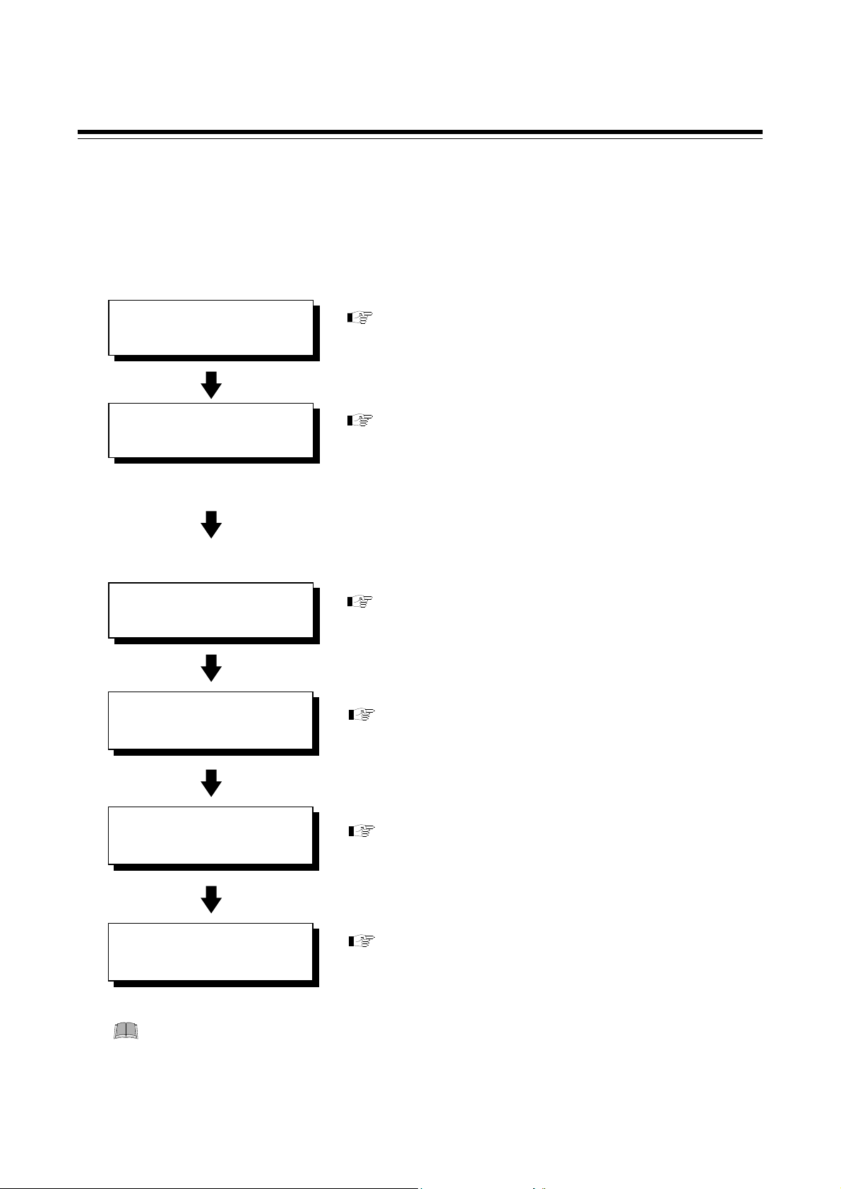
8. USAGE EXAMPLE
This chapter describes an usage example of PROFIBUS communication when connected with the
COM-JG and controller (SRZ) with the PLC set to a master.
8.1 Handling Procedures
Controller Address Setting
Preparations of
configuration instrument
Mounting and Wiring
Use Instrument Setting
Contents Check of
COM-JG Initial Setting
Refer to 8.2 System Configuration (P. 61)
• For mounting and wiring of the COM-JG, refer to
3. MOUNTING (P. 5) and 4. WIRING (P. 8).
For mounting and wiring of the controller (SRZ),
•
refer to Z-TIO INSTRUCTION MANUAL
(IMS01T01-E) or Z-DIO INSTRUCTION
MANUAL (IMS01T03-E).
For mounting and wiring of PLC, refer to PLC
•
Instruction Manual.
Refer to 8.3 Use Instruments Setting (P. 62)
Refer to 5.4 Controller Address Auto Obtain
Methods (P. 19)
Refer to 8.4 Contents Check of COM-JG Initial
Setting (P. 63)
PLC Tool Setting
To avoid error at operation start-up, COM-JG must be powered on LAST (after the
controller, PLC, etc.).
Refer to 8.5 PLC Tool Setting (P. 70) and
Instruction Manual of the Programming Software
STEP7.
60 IMR01Y35-E3
Page 67
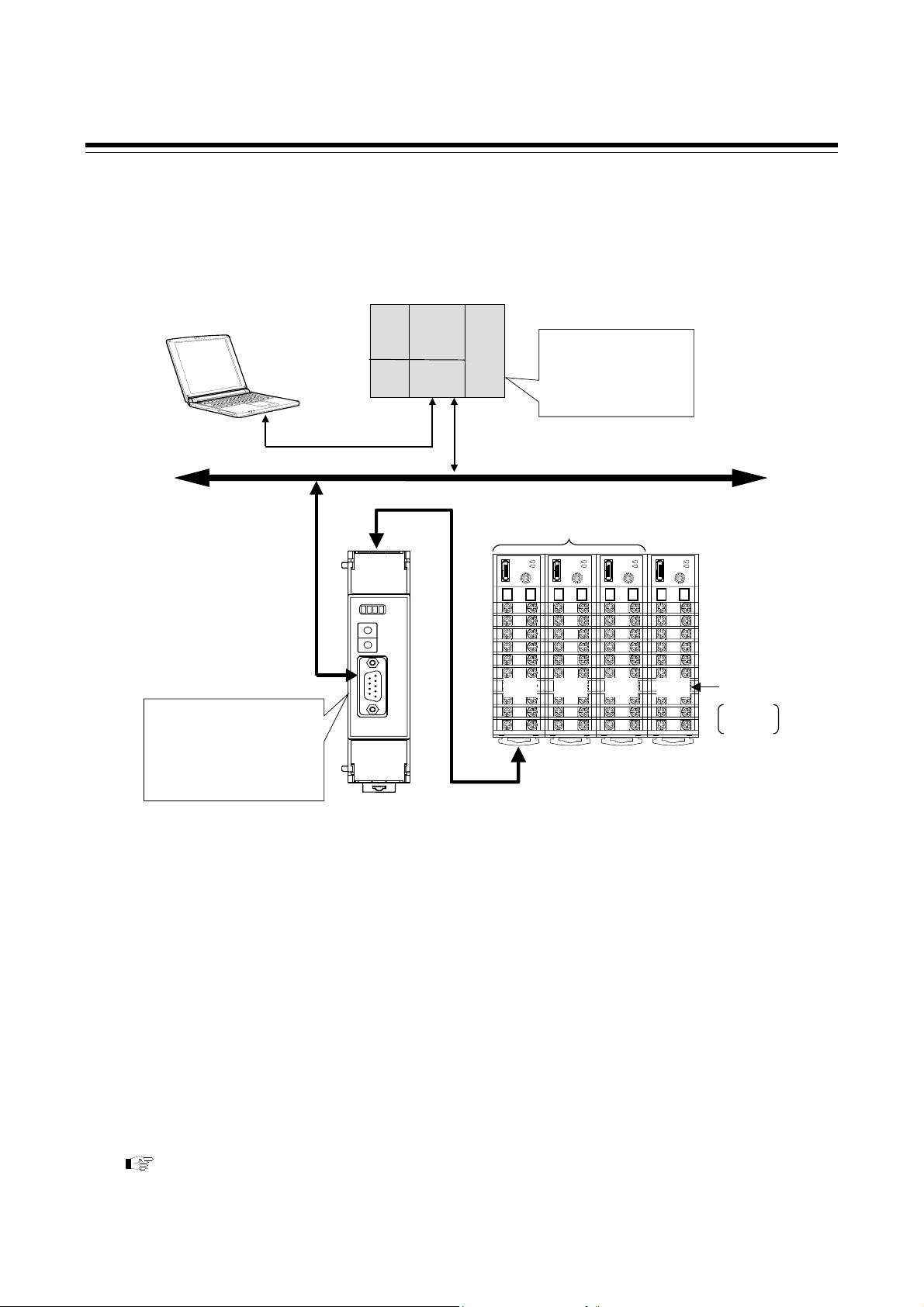
8.2 System Configuration
In this usage example, described the following system configuration.
Personal computer
Programmable controller
(PLC)
PROFIBUS-DP
8. USAGE EXAMPLE
SIEMENS
SIMATIC S7-300 series
(Master)
Communication speed:
12 Mbps
PROFIBUS communication
converter COM-JG
Remote I/O (Slave)
Address: 1
Communication speed:
12 Mbps
Z-TIO module
1 2 3 17
Controller (SRZ)
Controller communication
(RS-485: Modbus)
Z-DIO
module
Module
address
Controller
address
Use instruments
PROFIBUS communication converter: COM-JG............... 1
Controller (SRZ): Z-TIO module ...... 3 (4-channel type: 2, 2-channel type: 1)
Z-DIO module...... 1
PLC
SIMATIC S7-300 series (SIEMENS AG)
− Power supply module: PS-300 (PS307 2A) ..................... 1
− CPU module: S7-300 (CPU315-2DP) ............... 1
− Digital input module: DI-300 (SM321 DI16) ................ 1
Personal computer
Software of the following must be installed in a personal computer.
− Programming Software STEP7 V5.1 (SIEMENS AG)
For the personal computer to be connected to the PLC, refer to Instruction Manual of PLC
and STEP7.
IMR01Y35-E3
61
Page 68

8. USAGE EXAMPLE
8.3 Use Instruments Setting
Set the COM-JG and controller (SRZ) as the following.
There is not the hardware setting of PLC: SIMATIC S7-300 series (SIEMENS AG).
COM-JG setting
Set COM-JG to the following conditions.
• PROFIBUS address: 1
• Controller communication speed: 19200 bps (Factory set value)
For setting procedure, refer to 5. SETTING (P. 15).
Controller (SRZ) setting
• Module address: Z-TIO module: 4-channel type: 1, 2
2-channel type: 3
Z-DIO module: 17
The module address of a Z-TIO module will be the value
(decimal) set in the address setting switch plus “1.”
The module address of a Z-DIO module will be the value
(decimal) set in the address setting switch plus “17.”
• Communication protocol: Modbus-RTU
• Communication speed: 19200 bps (Factory set value)
• Data bit configuration: Data 8-bit, Without parity bit, Stop 1-bit
For setting method, refer to Z-TIO Host Communication Quick Instruction Manual
(IMS01T02-E) or Z-DIO INSTRUCTION MANUAL (IMS01T03-E).
62
IMR01Y35-E3
Page 69
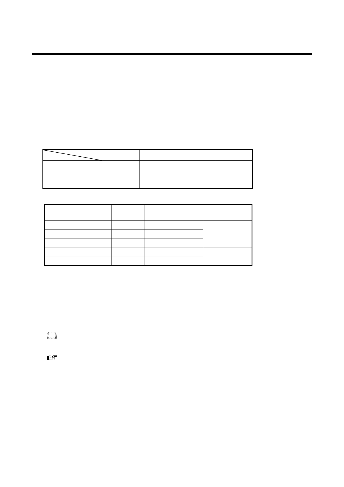
8. USAGE EXAMPLE
8.4 Contents Check of COM-JG Initial Setting
The contents of the COM-JG initial settings vary depending on the module configuration, number of
communication items, and communication content. For this reason, before using the PLC
configuration tool (Programming Software STEP7) to configure each setting, the module
configuration, number of communication items, and communication content required in the COM-JG
initial settings must be checked.
In this example, five communication items are set for the following module configuration.
Module configuration
Module type Z-TIO Z-TIO Z-TIO Z-DIO
Module address 1 2 3 17
Number of channels 4 4 2 8
Communication item
Communication item Attribute* Data type
Measured value (PV) RO Channel-based data
Set value (SV) R/W Channel-based data
RUN/STOP transfer R/W Module-based data
Digital input (DI) state RO Module-based data
RUN/STOP transfer R/W Module-based data
1st module 2nd module 3rd module 4th module
Corresponding
module
Z-TIO
Z-DIO
* RO: Read only, R/W: Read/Write
[COM-JG initial setting items]
• Controller address
• Number of continuous accesses
• Continuous accesses enable selection
• Static data read/write range
• Transmission wait time of controller communication
In this example, there is no need to set the “Transmission wait time of controller
communication.”
For COM-JG initial setting, refer to 5.3 COM-JG Initial Setting (P. 17).
IMR01Y35-E3
63
Page 70
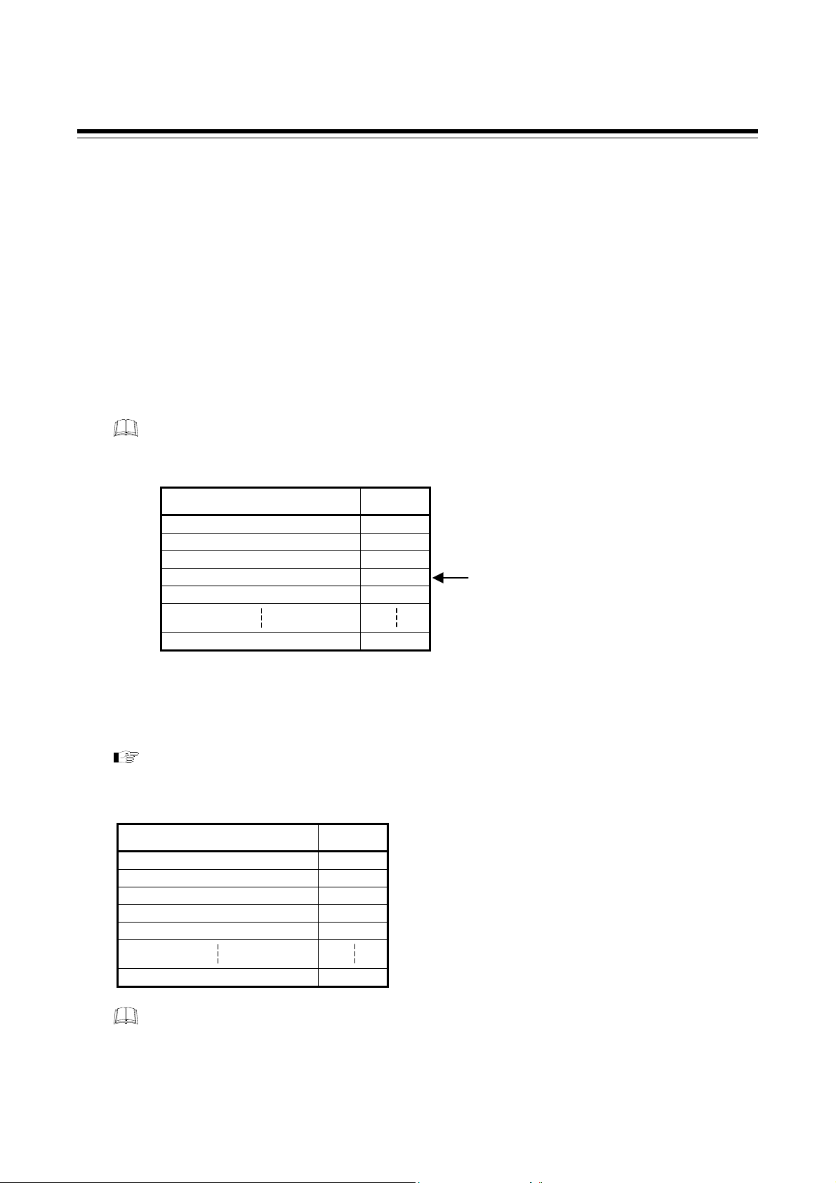
8. USAGE EXAMPLE
N
N
d
d
Controller address
Overview
To allow the PLC and COM-JG to communicate, the COM-JG must be made to recognize the address
of each controller (the module addresses of the SRZ).
Controller addresses can be obtained automatically by COM-JG DIP switch switching, or controller
addresses can be set using the PLC configuration tool.
Setting contents
Set each controller address (SRZ module address) in order from “No. 1 controller address” to “No. 31
controller address.”
Data range: 1 to 99 (0: No controller connected)
The COM-JG will not access controller address numbers following an address whose set
value is “0: No connected controller.”
Setting of usage example
In this example, the DIP switches switching of COM-JG are set so that controller addresses are
automatically obtained. Addresses are not set in the programming software STEP7.
[Example]
COM-JG initial setting item Set value
No. 1 Controller address 1
No. 2 Controller address 2
No. 3 Controller address 3
No. 4 Controller address 0
No. 5 Controller address 17
No. 31 Controller address 0
When No. 4 is set to “0: No connecte
controller”, settings for No. 5 and after are
invalidated (“17” in No. 5 is invalidated).
In this case, the number of connecte
controllers is three.
For controller address auto obtain, refer to 5.4 Controller Address Auto Obtain Methods
(P. 19).
“Controller address” setting
COM-JG initial setting item Set value
No. 1 Controller address 1
No. 2 Controller address 2
No. 3 Controller address 3
No. 4 Controller address 17
No. 5 Controller address 0
No. 31 Controller address 0
The controller address of a Z-TIO module will be the value (decimal) set in the address
setting switch plus “1.” The controller address of a Z-DIO module will be the value
(decimal) set in the address setting switch plus “17.”
64
o. 1 to No. 4 correspond to the 1st to the 4th module.
o modules are connected for No. 5 to No. 31, and thus
when addresses are automatically obtained, these are set
to “0: No connected controller.”
IMR01Y35-E3
Page 71
8. USAGE EXAMPLE
N
N
N
b
N
Number of continuous accesses
Overview
For a 4-channel type Z-TIO module, four register addresses will be allocated for one communication
item, for example when the Modbus register addresses of the measured value (PV) are 0000H to
0003H. When these are set using the PLC configuration tool, four items must be specified as static
data request items. However, if “Number of continuous accesses” is set to “4,” the static data request
item for all four channels can be set by simply specifying the item of the first register address.
Setting contents
For each module (No. 1 to No. 31), set the number of data of the communication item selected by the
static data request.
Data range: 1 to 85 (Factory set value: 4)
In a static data request, a combined total of up to 40 read and write items can be
communicated.
The factory set value for the number of continuous accesses is “4,” and thus when the
controller (SRZ) configuration consists only of 4-channel type Z-TIO modules, the setting
does not need to be configured.
As a basic rule, the “Number of continuous accesses” is set to the number of channels used
for each module. However, when only module-based data (such that one module has only
one data item) is set in the static data request (for example “Digital input (DI) state” of the
Z-DIO module), set the “Number of continuous accesses” to “1.”
Setting of usage example
In this example, there are other modules in addition to a 4-channel type Z-TIO module, and thus the
number of continuous accesses setting is required.
Communication item Modbus register address
Measured value (PV)
Set value (SV)
RUN/STOP transfer
Digital input (DI) state
RUN/STOP transfer
0000H to 0003H (0 to 3) Z-TIO
0008EH to 0091H (142 to 145) Z-TIO
006DH (109) Z-TIO
0000H (0) Z-DIO
0046H (70) Z-DIO
Corresponding
module
Data type
Channel-based
data
Module-based
data
For Modbus register address of the SRZ, refer to 7. COMMUNICATION DATA MAP (P. 28).
“Number of continuous accesses” setting
COM-JG initial setting item Set value
No. 1 Number of continuous accesses 4
No. 2 Number of continuous accesses 4
No. 3 Number of continuous accesses 2
No. 4 Number of continuous accesses 1
No. 5 Number of continuous accesses 4
o. 1 to No. 4 correspond to the 1st to the 4th module.
o. 4 (Z-DIO) has 8 channels, however, the data
specified for the Z-DIO module is all moduledata, and thus “1” is set.
o. 5 to No. 31 are not connected, and thus the settings
remain at “4,” the
factory set value.
o. 1 to No. 31 correspond to No. 1 to No. 31
ased
of "Controller address" in the COM-JG initial
No. 31 Number of continuous accesses 4
setting items.
IMR01Y35-E3
65
Page 72
8. USAGE EXAMPLE
Continuous accesses enable selection
Overview
The “Number of continuous accesses” is set for each controller (module), and thus when “4” is set,
each communication item of a module accesses four channels. However, some of the communication
items, such as “RUN/STOP transfer,” have only one data item per module. If four channels of data are
requested for this type of data, unnecessary register addresses will be accessed, and thus the “Number
of continuous accesses” setting should be disabled for module-based data.
Setting contents
Select whether or not the number of continuous accesses setting is enabled for each communication
item selected in a static data request.
When the number of continuous accesses setting is disabled, read and write are only performed with
respect to one register of the selected communication item.
Select enable/disable for each communication item of a static data request by bit. Eight items (8 bits)
is one byte, and thus the maximum of 40 items (Groups 1 to 40) is set using 5 bytes.
Data range: 0 to 255 (Factory set value: 255)
Groups 1 to 40 are divided into five sets of eight groups each, and enable/disable
continuous access is set by bit for each group.
Bit data 0: Continuous accesses disabled
1: Continuous accesses enabled
When only channel-based data is communicated, this setting is not necessary.
Setting of usage example
In this example, both module-based data and channel-based data are communicated, and thus the
continuous access enable select setting is necessary.
Read and write of a static data request are set as shown below.
• Read item: Z-TIO module: Measured value (PV), Set value (SV), RUN/STOP transfer
Z-DIO module: Digital input (DI) state, RUN/STOP transfer
• Write item: Z-TIO module: Set value (SV), RUN/STOP transfer
Z-DIO module: RUN/STOP transfer
Communication item
Display of
the PLC tool
Group 1 Measured value (PV) 0 (0000H)
Group 2 Set value (SV) 142 (008EH)
Group 3 RUN/STOP transfer 109 (006DH)
Group 4 Digital input (DI) state 0 (0000H)
Group 5 RUN/STOP transfer 70 (0046H)
Group 6 Set value (SV) 142 (008EH) Channel-based data
Group 7 RUN/STOP transfer 109 (006DH)
Group 8 RUN/STOP transfer 70 (0046H)
Group 9 ⎯ 65535 (FFFFH) ⎯ ⎯
Group 40 ⎯ 65535 (FFFFH) ⎯ ⎯
Name
Modbus
register
address
Data type
Channel-based data
Module-based data
Module-based data
Corresponding
module
Z-TIO
Z-DIO
Z-TIO
Z-DIO
Attribute
Read
Write
Continued on the next page.
66
IMR01Y35-E3
Page 73

8. USAGE EXAMPLE
Continued from the previous page.
Among the previously discussed communication items, there are three module-based items:
RUN/STOP
read and write of these items, disable the number of continuous accesses setting.
Continuous accesses enable/disable setting of Group 1 to 8
Validate (1)/Invalidate (0) 0 0 1 0 0 0 1 1
transfer (Z-TIO), Digital input (DI) state (Z-DIO), and RUN/STOP transfer (Z-DIO). For
Group No.
Group 8
(Bit 7)
Group 7
(Bit 6)
Group 6
(Bit 5)
Group 5
(Bit 4)
Group 4
(Bit 3)
Group 3
(Bit 2)
Group 2
(Bit 1)
A lower bit is Group 1.
Group 1
(Bit 0)
The value of “Continuous access enable selection” of Groups 1 to 8 is 00100011 = 35
Groups 9 to 16, Groups 17 to 24, Groups 25 to 32, and Groups 33 to 40 do not use this setting, and
thus the factory set value of 255 (all enabled) should remain unchanged.
Group No. Group 1 to 8 Group 9 to 16 Group 17 to 24 Group 25 to 32 Group 33 to 40
Set value 35 255 255 255 255
Therefore, the continuous access enable selection setting is set as shown below.
“Continuous access enable selection” setting
COM-JG initial setting item Set value
Continuous access enable selection 1 to 8 35
Continuous access enable selection 9 to 16 255
Continuous access enable selection 17 to 24 255
Continuous access enable selection 25 to 32 255
Continuous access enable selection 33 to 40 255
IMR01Y35-E3
67
Page 74

8. USAGE EXAMPLE
Static data read/write range
Overview
The static data read/write range can be set to prevent the reading of unneeded data and the writing of
incorrect data.
When a communication item is specified in a static data request, a read or write request is normally
sent to the same Modbus register address of all connected controllers (each module of the SRZ).
For this reason, when modules that have different Modbus register addresses are connected and a
communication item is specified, the wrong data may be read or data may be written to other than the
intended communication item (depending on the module).
For example, when a Z-TIO module and a Z-DIO module of an SRZ are connected and a
communication item of the Z-TIO module is read, the data of the same Modbus register address
in the Z-DIO module as the communication item specified in the Z-TIO module is read. However,
because the contents of the Modbus register addresses of the Z-TIO module and the Z-DIO
module are different, different data is read from each.
Example Z-TIO module: 006DH → RUN/STOP transfer
Z-DIO module: 006DH → DO minimum ON/OFF time of proportioning cycle
To avoid having unnecessary data read, the range of data that can be communicated for the same
module type can be assigned.
Setting contents
Five channels each can be set for read and write. This means that five different types of Modbus
register addresses can be handled.
For each channel, set the number of connected modules that have the same Modbus register address
and the number of communication items.
Data range: 0 to 65535 (Factory set value: 0)
The “Number of connected modules” is set in the upper hexadecimal byte, and the
“Number of communication items” is set in the lower byte.
This setting is not necessary when the controller consists only of modules that are the same
type.
For Modbus register address of the SRZ, refer to 7. COMMUNICATION DATA MAP
(P. 28).
68
IMR01Y35-E3
Page 75
8. USAGE EXAMPLE
d
N
Setting of usage example
In this example, the Modbus register addresses of the connected Z-TIO and Z-DIO modules each have
different contents, and thus the static data read/write range setting is required.
To enable static data read/write access by module, it is recommended that a table be created that shows
the correspondence between communication item groups and controller addresses.
For one type of module, set the validate data range to one channel for read and one channel for write.
Communication
item
Controller address
No. 1 No. 2 No. 3 No. 4
Corresponding
module
Group 1
Group 2
Z-TIO Read CH1
Group 3
Group 4
Group 5
Group 6
Group 7
Z-DIO Read CH2
Z-TIO Write CH1
Group 8 Z-DIO Write CH2
Static data
read/write
range channel
o. 1 to No. 4
correspond to
the 1st to the 4th
module.
: Validate data
: Static data read/write range
In the above table, two channels are set for read and two channels are set for write. The “Number of
connected modules” is set in the upper hexadecimal byte, and the “Number of communication items”
is set in the lower byte.
Static data
read/write
range channel
Number of
connection modules
(Set value upper-byte)
Number of
communication items
(Set value lower-byte)
Set value
Read CH1 3 3 0303H (771)
Read CH2 1 2 0102H (258)
Write CH1 3 2 0302H (770)
Write CH2 1 1 0101H (257)
Based on the above, the static data read range and the static data write range are set as shown below.
“Static data read/write range” setting
COM-JG initial setting item Set value
Static data read range CH1 0303H (771)
Static data read range CH2 0102H (258)
Static data read range CH3 0
Static data read range CH4 0
Static data read range CH5 0
Static data write range CH1 0302H (770)
Static data write range CH2 0101H (257)
Static data write range CH3 0
Static data write range CH4 0
Static data write range CH5 0
Static data read ranges CH3 to CH5 an
static data write ranges CH3 to CH5 are
not used, and thus the set value is “0.”
IMR01Y35-E3
69
Page 76

8. USAGE EXAMPLE
8.5 PLC Tool Setting
This section explains the procedures for using the programming software STEP7 to configure settings.
8.5.1 Setting procedures
COM-JG initial setting
The procedure for configuring COM-JG initial settings is explained below.
Before configuring COM-JG initial settings, be sure to set DIP switch No. 7 to ON
(controller communication disabled). After you have completed the COM-JG initial
settings, be sure to return DIP switch No. 7 to OFF (controller communication enabled).
(Refer to page 17)
Starting the Programming
Software STEP7
Creating a new project
Register a GSD file
PLC master setting
Register a COM-JG
Starting the COM-JG
initial setting
Repeat the following procedure (from “Data parameter setting” to “Monitor and
modify of variable”) for each setting item.
[COM-JG initial setting items]
・Number of continuous accesses ・Static data read range
・Continuous accesses enable selection ・Static data write range
Data parameter setting
Continued on the next page.
Refer to 8.5.2 General procedures
Creating a new project (P. 73)
Refer to 8.5.2 General procedures
Register a GSD file (P. 76)
Refer to 8.5.2 General procedures
PLC master setting (P. 78)
Refer to 8.5.2 General procedures
Register a COM-JG (P. 81)
Refer to 8.5.3 COM-JG initial setting
Data parameter setting (P. 83)
70
IMR01Y35-E3
Page 77

8. USAGE EXAMPLE
Continued from the previous page.
Configuration setting
Refer to 8.5.3 COM-JG initial setting
Configuration setting (P. 86)
Save and compilation
of project
Refer to 8.5.3 COM-JG initial setting
Save and compilation of project (P. 90)
Creating a variable table
Refer to 8.5.3 COM-JG initial setting
Creating a variable table (P. 91)
Monitor and modify
of variable
Refer to 8.5.3 COM-JG initial setting
Monitor and modify of variable (P. 97)
To Communication
item setting
Refer to 8.5.4 Communication item
setting (P. 102)
In the COM-JG initial settings, the number of data that is read or written varies by setting
item and thus the procedure must be repeated for each setting item. However, when the
number of data read or written is the same, such as for “Static data read range” and “Static
data write range”, the settings can be configured together.
For details, refer to Instruction Manual of the Programming Software STEP7.
IMR01Y35-E3
71
Page 78

8. USAGE EXAMPLE
Communication item setting
The procedure for configuring communication item settings is shown below.
Starting the Programming
Software STEP7
Creating a new project
Refer to 8.5.2 General procedures
Creating a new project (P. 73)
PLC master setting
Refer to 8.5.2 General procedures
PLC master setting (P. 78)
Register a COM-JG
Refer to 8.5.2 General procedures
Register a COM-JG (P. 81)
Data parameter setting
Refer to 8.5.4 Communication item setting
Data parameter setting (P. 102)
Configuration setting
Refer to 8.5.4 Communication item setting
Configuration setting (P. 105)
Save and compilation
of project
Refer to 8.5.4 Communication item setting
Save and compilation of project (P. 112)
Download a project
to the PLC
For details, refer to Instruction Manual of the Programming Software STEP7.
72 IMR01Y35-E3
Page 79

8. USAGE EXAMPLE
8.5.2 General procedures
When configuring either COM-JG initial settings or communication item settings, first follow the
general procedures below.
Registering a GSD file is only performed when configuring COM-JG initial settings; it is not
necessary when configuring communication item settings.
Creating a new project
When configuring communication item settings, you can save the project that you created
when configuring COM-JG initial settings under a different name. This will enable you to
omit “PLC master setting” and “Register a COM-JG.”
1. Start programming software STEP7.
2. Select the menu command File → N
In this example, the project name is “COM-J.”
When configuring communication item settings, use a different project name than the
project name you used for COM-JG initial settings.
Project Name
ew…, and creating a new project.
IMR01Y35-E3
73
Page 80
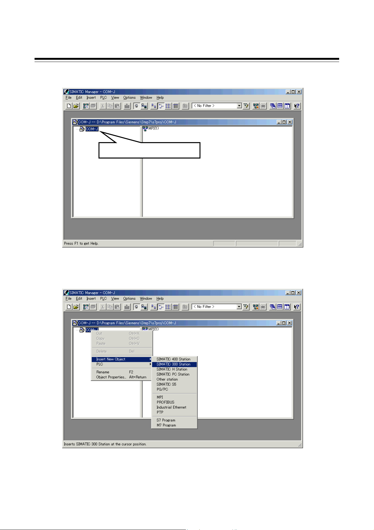
8. USAGE EXAMPLE
3. Clicking “OK” displays the new project on the SIMATIC Manager.
The project that was created
4. The PLC is registered to the created object.
In this example, select “SIMATIC 300 Station.”
74
IMR01Y35-E3
Page 81

5. If the PLC is registered, the display becomes as follows.
8. USAGE EXAMPLE
IMR01Y35-E3
75
Page 82

8. USAGE EXAMPLE
Register a GSD file
Registering a GSD file is only performed when configuring COM-JG initial settings; it is not
1. To link COM-JG to the project, register the GSD file for COM-JG downloaded from the RKC
necessary when configuring communication item settings.
official website. Click the “SIMATIC 300” folder on the screen registered with the PLC and then
double-click “Hardware” on the right side of the window.
Double-click
Station editing
window
76
Hardware catalog
window
Rack detail window
IMR01Y35-E3
Page 83
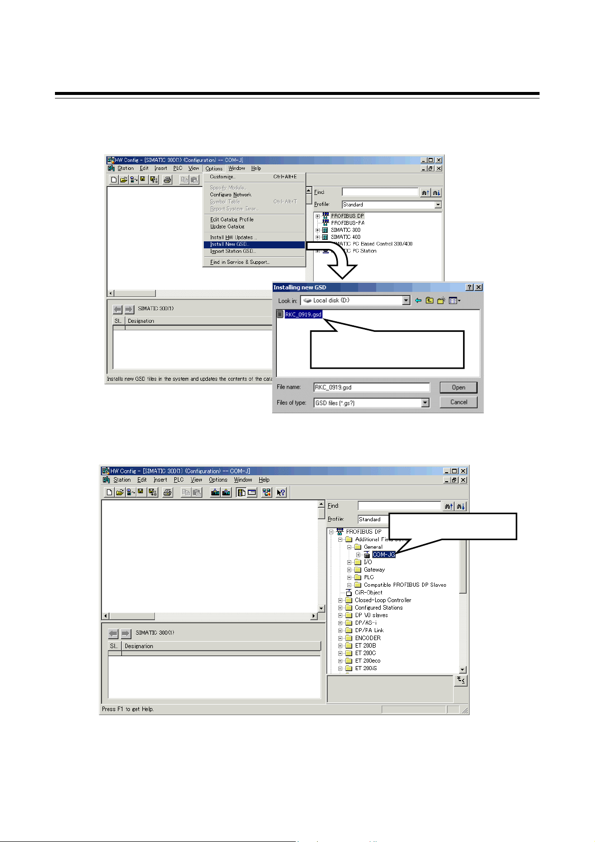
8. USAGE EXAMPLE
2. Go to the “Options” on the menu bar and click on “Install New GSD…” to register GSD file for
COM-JG downloaded from the RKC official website.
Select GSD file of COM-JG.
File name: RKC_0919.gsd
3. After the GSD file is registered, “COM-JG” is displayed on the HW configuration screen.
COM-JG is displayed
IMR01Y35-E3
77
Page 84

8. USAGE EXAMPLE
PLC master setting
Example:
1. Double-click Rail under “RACK-300” in the folder tree to display rack (RACK).
Rack (RACK)
appears.
Select “Rail”
2. Drag and drop “PS 307 2A” of the power supply module, “PS-300” within the rack.
Drag & drop
78
IMR01Y35-E3
Page 85

8. USAGE EXAMPLE
3. Succeeding drag and drop “6ES7-315-2AF00-0AB0” of the CPU module, “CPU 315-2 DP.”
Drag & drop
4. As the properties are displayed, click “New…” to set the network.
In this example, the “Highest PROFIBUS Address” is set to 126 and the “Transmission Rate,” to
12Mbps.
Click
IMR01Y35-E3
79
Page 86
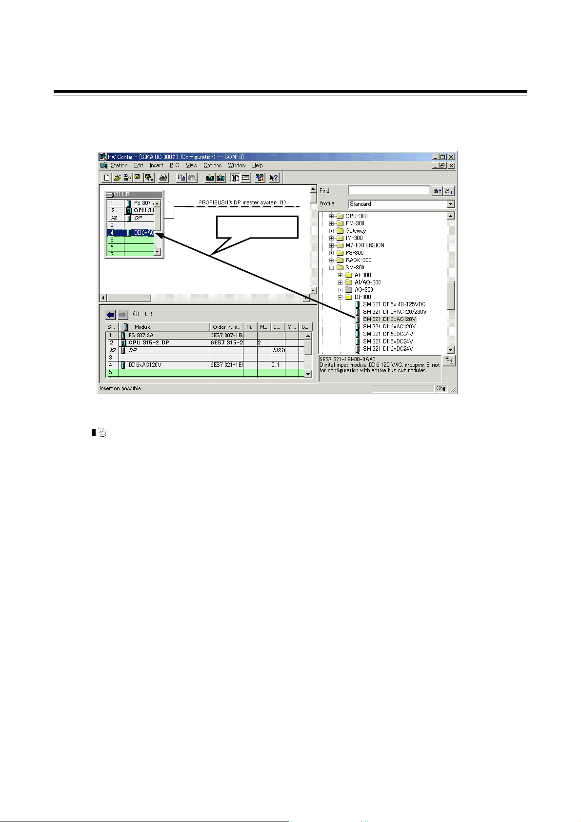
8. USAGE EXAMPLE
5. Drag and drop “SM 321 DI16xAC120V” of the DI module, “DI-300.”
Thus, the PLC hardware setting has been finished.
Drag & drop
For details of the procedure for adding the rack, and Power supply, CPU and Digital input
modules and for defining the PROFIBUS master, refer to the instruction manual for
Programming Software STEP7.
80
IMR01Y35-E3
Page 87

8. USAGE EXAMPLE
Register a COM-JG
1. Drag and drop “COM-JG” onto “PROFIBUS (1): DP master system (1)” from the hardware
catalog.
Drag & drop
2. As the properties are displayed, set the PROFIBUS address.
In this example, “1” is set.
Sets “1”
IMR01Y35-E3
81
Page 88

8. USAGE EXAMPLE
3. If the COM-JG is registered, the display becomes as follows.
This concludes the general procedures.
82
IMR01Y35-E3
Page 89
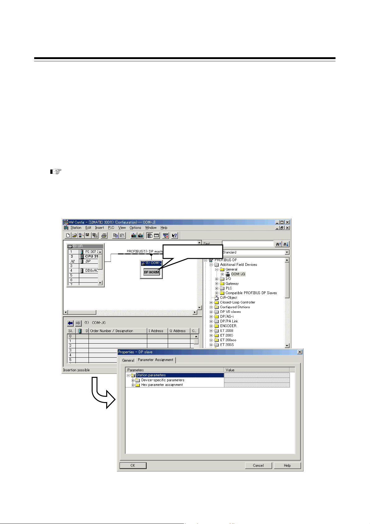
8. USAGE EXAMPLE
8.5.3 COM-JG initial setting
The following four items are set as COM-JG initial setting items.
• Number of continuous accesses
• Continuous accesses enable selection
• Static data read range
• Static data write range
Repeat the following procedure [from Data parameter setting (P. 83) to Monitor and modify of
variable (P. 97)] for each initial setting item. The example below explains how to set the “Number of
continuous accesses.”
Refer to 8.4 Contents Check of COM-JG Initial Setting (P. 63).
Data parameter setting
1. Double-click “COM-JG” registered to set each controller (SRZ) communication item.
Double-click
IMR01Y35-E3
83
Page 90

8. USAGE EXAMPLE
2. Set the number of data of the communication item in “Number of Channel” in “Device-specific
parameters.” In this example, “4” is set for the “Number of continuous accesses” (because there
are four modules).
For “Continuous access enable selection,” “Static data read range,” and “Static data write
range,” set “5.”
Sets “4”
3. Set the number of read/write items to “Group read/write allocation.”
In this example, the number of read items set to 1, and the number of write items, to 39.
The number of items that can be set by the COM-JG is 40 maximum including both read
and write items.
If you are setting “Static data read range” and “Static data write range” at the same time,
set 2 read items and 38 write items.
Sets as 1 read item and
39 write items
84
IMR01Y35-E3
Page 91
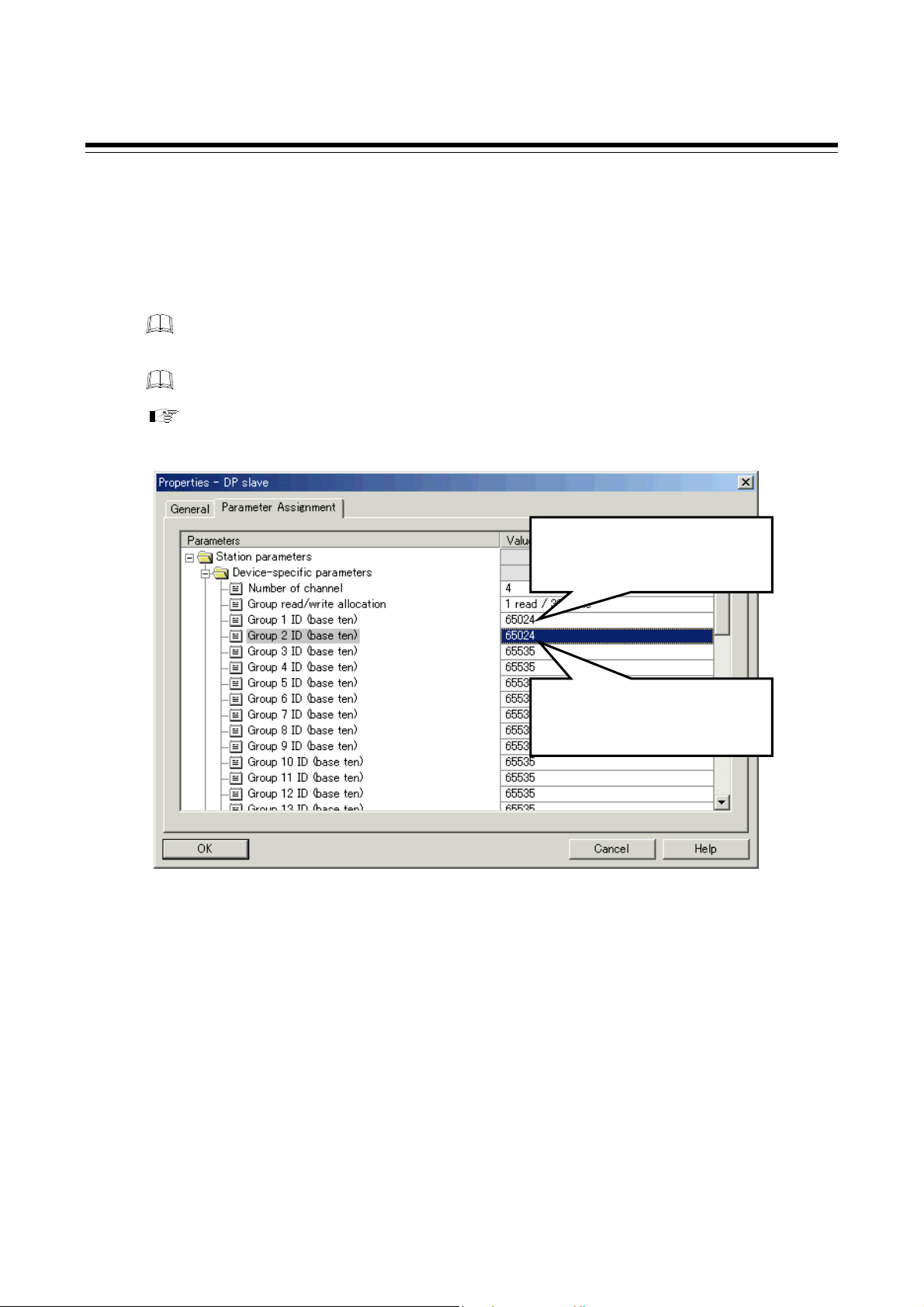
4. Set read and write items in order from “Group 1 ID (base ten).”
The set value sets the Modbus register address of the controller (SRZ) connected in a decimal
number. In this example, make the setting as follows.
Read item: Group 1 ID (base ten): 65024 (No. 1 Number of continuous accesses)
Write item: Group 2 ID (base ten): 65024 (No. 1 Number of continuous accesses)
Because the number of read items is set to “1,” a read item can only be set for Group 1 ID
(base ten). Write items must be set for Group 2 ID (base ten) and following groups.
Blank items will be the factory set value “65535.”
For Modbus register address of COM-JG initial setting items, refer to 7.5 COM-JG
Initial Setting Items (P. 58).
8. USAGE EXAMPLE
5. After the allocation of data parameters is finished, click “OK.”
Set “65024: No. 1 Number
of continuous
the read item.
accesses” as
Set “65024: No. 1 Number
of continuous accesses” as
the write item.
IMR01Y35-E3
85
Page 92

8. USAGE EXAMPLE
Configuration setting
1. Select “COM-JG” and then set the write permission flag register.
Select “Write permission” from the hardware catalog and then drag and drop it to the COM-JG
rack detail window.
Always set “Write permission” regardless of the contents of communication items.
In addition, always set “Write permission” to the first line.
In this example, the error state register (“Error state”) setting is omitted. If you set the
error state register (“Error state”), be sure to set it on the first line. (“Write permission”
will be on the second line.)
In the COM-JG initial settings, the write control flag register (“Write control”) is not
used.
Drag & drop
86
IMR01Y35-E3
Page 93

2. Set the number of the word of static data.
Read/writes, data length of one item become a single word.
Number of read words = Number of communication items × Number of read items
= 4 × 1 = 4
Number of write words = Number of communication items × Number of write items
= 4 × 1 = 4
Select “Static input word” and “Static output word” from the hardware catalog and then drag and
drop it to the COM-JG rack detail window. 1/2/4/8/16 words are available.
In this example, the number of data of “Number of continuous accesses” is “4” (there are four
modules) and the number of read and write items is one each. Thus four words are set for both
read and write.
Always locate “Static input word” above “Static output word” on the rack detail
window.
8. USAGE EXAMPLE
Select and then set the number of word of the COM-JG initial setting from among 1, 2, 4,
8 and 16 words so that the total number of words becomes the same as “Number of
communication items × Number of read (or write) items.”
For example, if “Number of communication items × Number of read items.” Corresponds
to five words, select one word and four words.
Select the number of
the word of read data,
and do drag & drop
IMR01Y35-E3
Select the number of
the word of write data,
and do drag & drop
87
Page 94
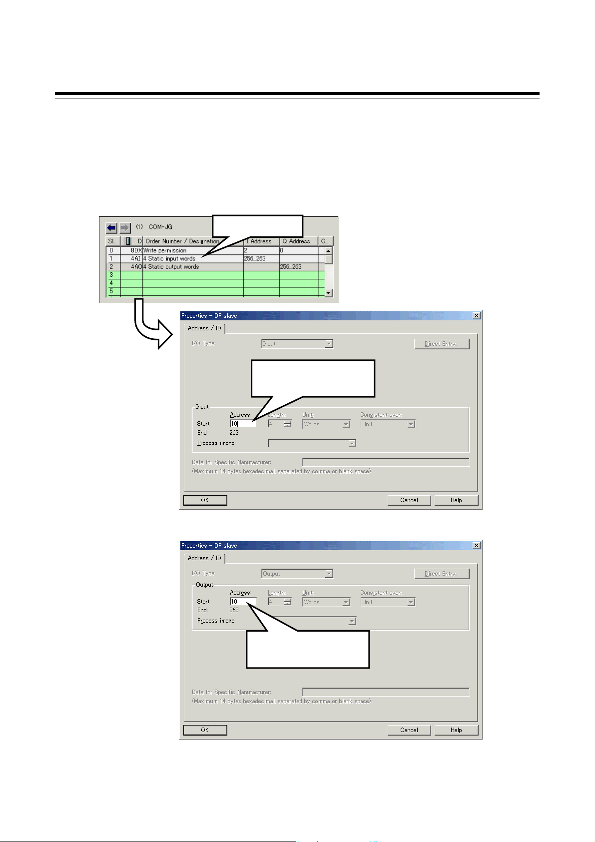
8. USAGE EXAMPLE
3. Set the PLC register address for static data read and write requests.
Double-click the “Static input word” cell and the “Static output word” cell in the COM-JG rack
detail window, and set the starting address.
In this example, make the setting as follows.
4 Static input words: Input Start address: 10
4 Static output words: Output Start address: 10
Double-click
Set the start address
of read request
Read address
Set the start address
of write request
Write address
88
IMR01Y35-E3
Page 95

8. USAGE EXAMPLE
When set the number of the word of dynamic data
Select “Dynamic I/O word” for step 2 and then drag and drop it to the COM-JG rack detail
window. 1/2/4/ words are available.
In this example, select “1 Dynamic I/O word.”
Drag & drop
Set the
PLC register address for dynamic data read and write requests.
Double-click “1 Dynamic I/O word” of COM-JG rack detail window, and then sets the start
address.
In this example, set “100.”
Set the start address
of write request
IMR01Y35-E3
Set the start address
of read request
89
Page 96

8. USAGE EXAMPLE
Save and compilation of project
1. Click the “Save and Compile” button on the toolbar, and save and compilation of the project.
Click the “Save and Compile”
button
2. Click the “Download to Module” button on the toolbar, and download a project to the PLC.
If normally downloaded, the window to inform the operator of the progress opens, and then
returns to the window for hardware configuration.
Click the “Download to Module”
button
90 IMR01Y35-E3
Page 97

8. USAGE EXAMPLE
Creating a variable table
Use the variable monitor/modify function of STEP7 to write the COM-JG initial setting item to
COM-JG. Create a variable table to monitor and modify variables.
1. Selects “Block” from the tree of SIMATIC Manager. Right-click on the “Block” and select the
command Insert New Object → Variable Table.
Right-click
2. Input a symbol name, and click OK.
In this example, the symbol name is “COM-JG setting.”
Input a symbol name
IMR01Y35-E3
91
Page 98
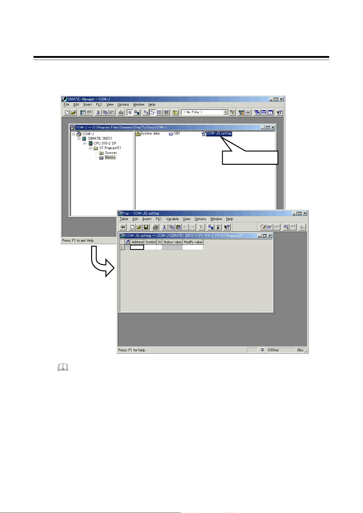
8. USAGE EXAMPLE
3. Double-click the icon of the created symbol name “COM-JG setting” to display a variable table
as shown the table below.
Double-click
The Enter key can be pressed to increase the number of entry lines. The last line will not
contain an entry.
92
IMR01Y35-E3
Page 99
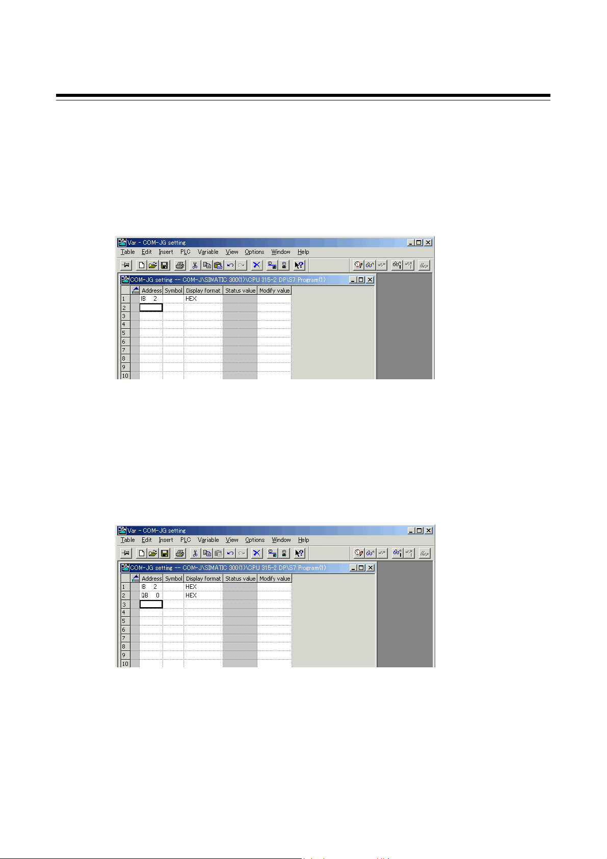
4. Set the read item of write permission flag register.
In the configuration settings, the PLC register addresses of the write permission flag register
(“Write permission”) are set as follows:
Input Start address (I Address): 2
End address (I Address): 2 (Automatically assigned)
As such, set “IB2” in “Address” of the variable table.
(IB2: A one-byte data area is allocated in address 2 and the data of address 2 is read.)
8. USAGE EXAMPLE
5. Set the write item of write permission flag register.
In the configuration settings, the PLC register addresses of the write permission flag register
(“Write permission”) are set as follows:
Output Start address (Q Address): 0
End address (Q Address): 0 (Automatically assigned)
As such, set “QB0” in “Address” of the variable table.
(QB0: A one-byte data area is allocated in address 0 and the data of address 0 is written.)
IMR01Y35-E3
93
Page 100
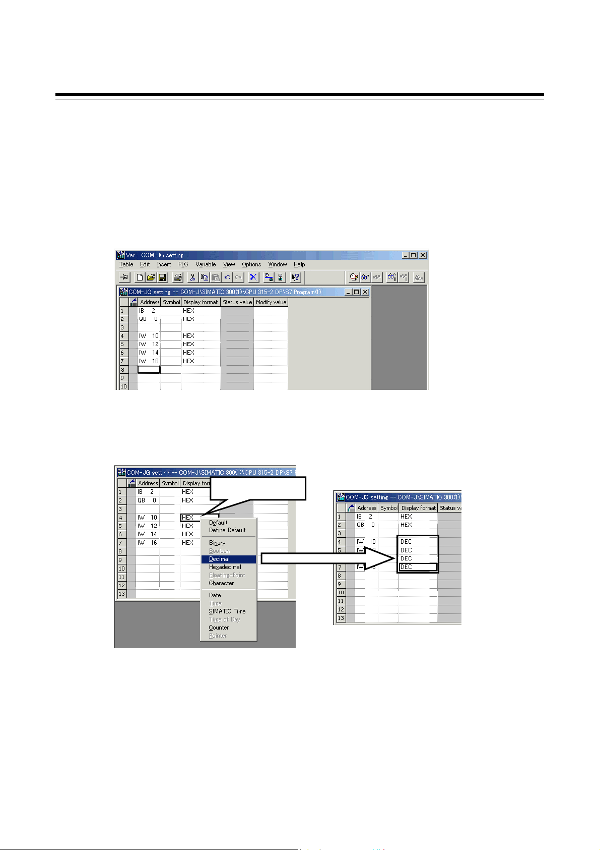
8. USAGE EXAMPLE
6. Set the static data read request items.
In the configuration settings, the PLC register addresses of the static data read request item
(“Static input word”) are set as follows:
Input Start address (I Address): 10
End address (I Address): 17 (Automatically assigned)
As such, set “IW10,” “IW12,” “IW14,” and “IW16” in “Address” of the variable table.
(IW10: A one-byte data area [address 10 and 11] is allocated in address 10 and the data of address
10 is read.)
7. Change the display format of “IW10,” “IW12,” “IW14,” and “IW16” from HEX to DEC.
Right-click a cell that shows HEX and select “Decimal” from the sub-menu to change to DEC.
Right-click
94
IMR01Y35-E3
 Loading...