RICOH RV5VH101-E1, RV5VH101-E2, RV5VH102-E1, RV5VH102-E2, RV5VH201-E1 Datasheet
...
APPLICATION MANUAL
DC/DC CONVERTER
CONTROLLER
RV5VH SERIES
NO. EA-049-0006

1
DC/DC CONVERTER CONTROLLER
RV5VH SERIES
OUTLINE
Each of the RV5VH series is dual output CMOS DC/DC converter ICs integrating Step-up and inverting DC/DC converters.
The RV5VH3
××series ICs consists of an oscillator, two VFM control circuits, control transistors(EXT switches), a phase
shift circuit, a voltage reference unit, an error amplifier, and voltage sensing resistors. The package for the RV5VH series
is 8pin SSOP(0.65mm pitch), and it is suitable for power supply systems with positive and negative output, such as pager,
PDA, which need power supplies for LCD.
RV5VH1
××and RV5VH2×× series are able to provide two DC/DC converters, one is a step-up DC/DC converter with
internally fixed output and the other is an inverting DC/DC converter with adjustable output by external resistors. A voltage detector with sensing pin is also included. RV5VH3
××series are able to provide two DC/DC converters, both of them
require external drivers, DC/DC1, and inverting one, DC/DC2, can be adjustable by resistors.
FEATURES
• Dual DC/DC converter system
.................................
DC/DC1 : step-up
DC/DC2 : inverting(negative voltage)
• Voltage Detector
..........................................................
Nch. Open Drain Output
• Low voltage operation available
RV5VH1
××,RV5VH2××
..........................................
oscillator start-up from 0.8V
RV5VH3
××
.................................................................
oscillator start-up from 1.8V
• High Efficiency
.............................................................
TYP. 80%
• Low Supply Current
• High accuracy feedback sensing
...............................
TYP. ±2.5%
• Sleep Mode
RV5VH1
××, RV5VH2××
..........................................
DC/DC 2
RV5VH3
××
.................................................................
DC/DC1, 2
• Available to adjust temperature drift
.........................
DC/DC2 : with external resistor (RV5VH2
××, RV5VH3××)
coefficient of output voltage
• Small Package
..............................................................
8pin SSOP(0.65mm pitch)
APPLICATIONS
• Power source for telecommunication systems
• Power source for portable data processing systems, e.g. PDA, Electronic Data Banks
• Power source for Audio-Visual systems, e.g. CD players, Video cameras
• Power source for Notebook PCs, Word processing systems
• Gadgets which need two power supplies, e.g. CPU and LCD
2
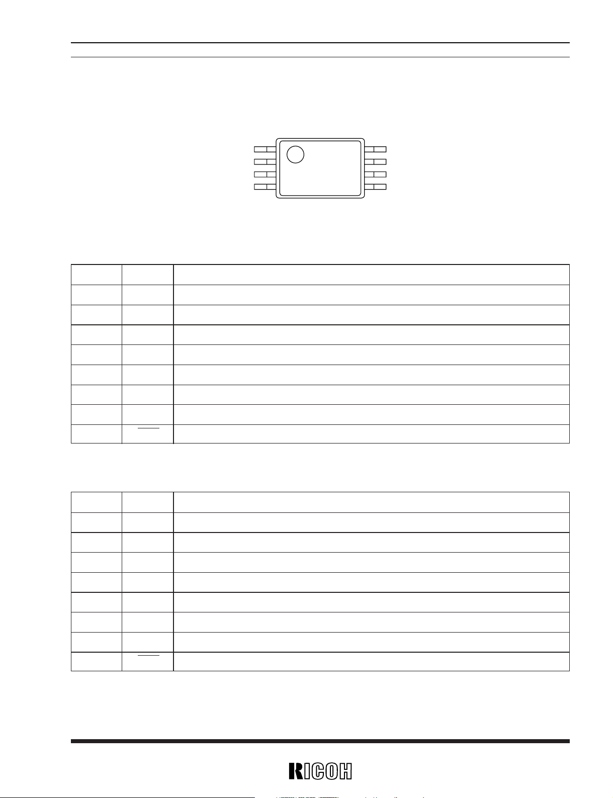
BLOCK DIAGRAM
+
–
+
–
CSW
V
SEN
VOUT1
LX1
DOUT
FB
EXT2
GND
Vref
Error Amp.1
Error Amp.2
1
2
3
4
8
7
6
5
VFM2
V
LX lim.
VFM1 OSC
p_shift
+
–
DC/DC CONVERTER CONTROLLER
(BOOST / INVERTING)
RV5VH1××/ RV5VH2××
• RV5VH1××
+
–
+
–
CSW
V
SEN
VOUT1
EXT1
D
OUT
FB
EXT2
GND
Vref
Error Amp.1
Error Amp.2
1
2
3
4
8
7
6
5
VFM2
VFM1 OSC
p_shift
+
–
• RV5VH2××
3
RV5VH1××/RV5VH2××
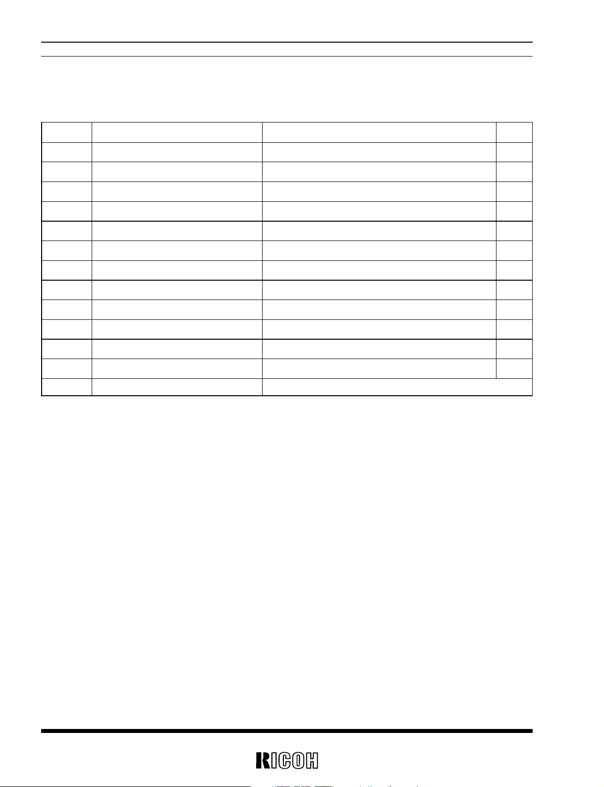
PIN CONFIGURATION
1
2
3
4
8
7
6
5
• 8 pin SSOP (0.65mm pitch)
PIN DESCRIPTION
• RV5VH1××
Pin No. Symbol Description
1 CSW Control switch for DC/DC2
2VSEN Sensing Pin for Voltage Detector
3VOUT1 Output for DC/DC1, Power supply for the device
4LX1 Output for DC/DC1, switching (Nch Open-Drain)
5 GND Ground
6 EXT2 External Transistor drive pin for DC/DC2 (CMOS output)
7 FB Input for DC/DC2 Error Amplifier
8D
OUT Output for Voltage detector
• RV5VH2××
Pin No. Symbol Description
1 CSW Contol switch for DC/DC2
2VSEN Sensing Pin for Voltage Detector
3VOUT1 Output for DC/DC1, Power supply for the device
4 EXT1 External Transistor drive pin for DC/DC1 (CMOS output)
5 GND Ground
6 EXT2 External Transistor drive pin for DC/DC2 (CMOS output)
7 FB Input for DC/DC2 Error Amplifier
8D
OUT Output for Voltage Detector
RV5VH1××/RV5VH2××
4
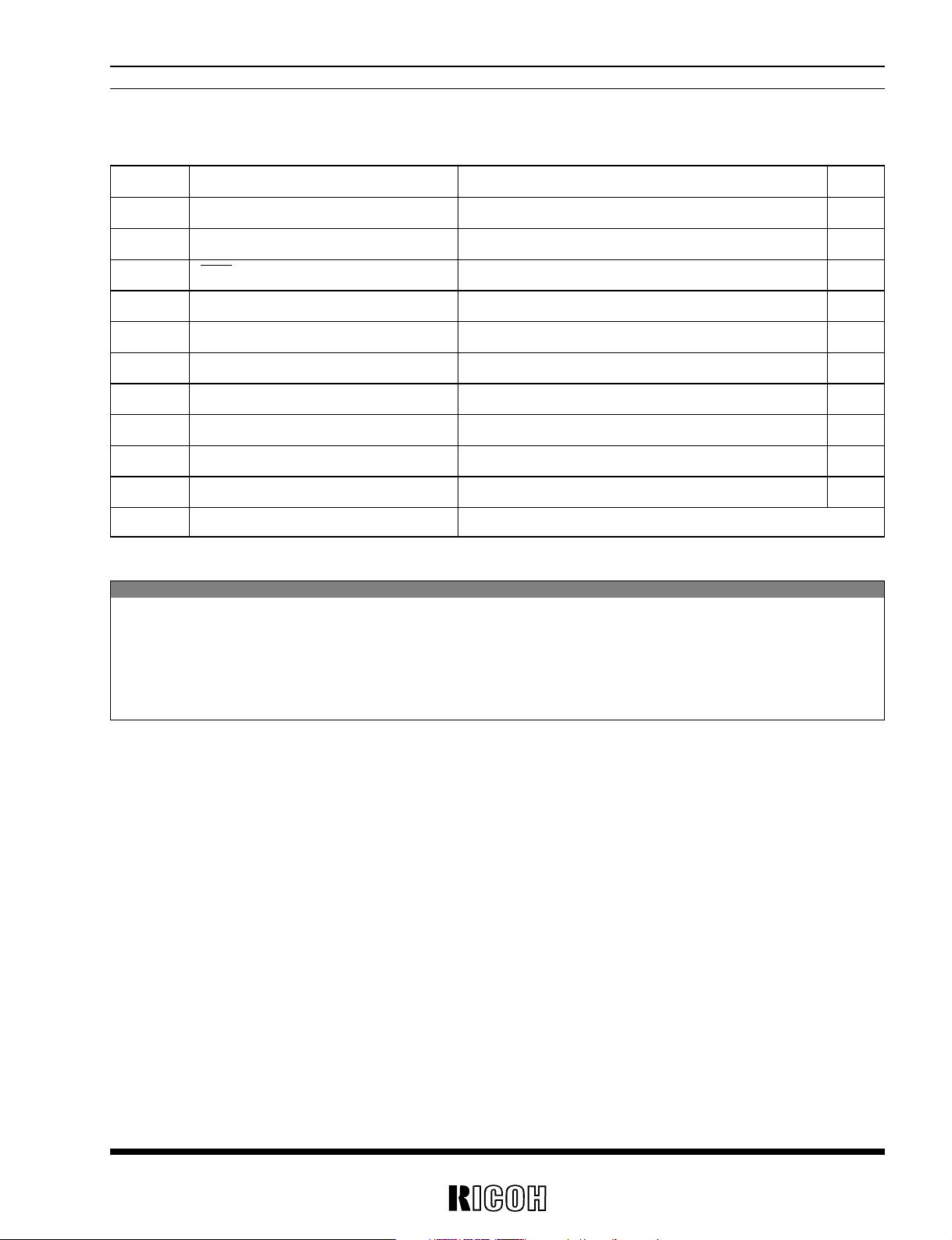
ABSOLUTE MAXIMUM RATINGS
• RV5VH1××
Symbol Item Ratings Unit
VOUT1 VOUT1 Pin Voltage 12 V
VLX1 LX1 Pin Voltage 12 V
VSEN VSEN Pin Voltage 12 V
DOUT DOUT Pin Voltage 12 V
VCSW CSW Pin Voltage –0.3 to VOUT1 +0.3 V
VEXT2 EXT2 Pin Voltage –0.3 to VOUT1 +0.3 V
VFB FB Pin Voltage –0.3 to VOUT1 +0.3 V
ILX1 LX1 Output Current 400 mA
IEXT2 EXT2 Output Current ±50 mA
PD Power Dissipation 300 mW
Topt Operating Temperature –40 to +85 ˚C
Tstg Storage Temperature –55 to +125 ˚C
Tsolder Lead Temperature (Soldering) 260˚C 10sec
5
RV5VH1××/RV5VH2××
ABSOLUTE MAXIMUM RATINGS
Absolute Maximum ratings are threshold limit values that must not be exceeded even for an instant under
any conditions. Moreover, such values for any two items must not be reached simultaneously. Operation
above these absolute maximum ratings may cause degradation or permanent damage to the device. These
are stress ratings only and do not necessarily imply functional operation below these limits.
• RV5VH2××
Symbol Item Ratings Unit
VOUT1 VOUT1 Pin Voltage 12 V
VSEN VSEN Pin Voltage 12 V
DOUT DOUT Pin Voltage 12 V
VCSW CSW Pin Voltage –0.3 to VOUT1 +0.3 V
VEXT1, 2 EXT1, 2 Pin Voltage –0.3 to VOUT1 +0.3 V
VFB FB Pin Voltage –0.3 to VOUT1 +0.3 V
IEXT1, 2 EXT1, 2 Output Current ±50 mA
PD Power Dissipation 300 mW
Topt Operating Temperature –40 to +85 ˚C
Tstg Storage Temperature –55 to +125 ˚C
Tsolder Lead Temperature (Soldering) 260˚C 10sec
RV5VH1××/RV5VH2××
6
ELECTRICAL CHARACTERISTICS
• RV5VH101
DC/DC Converter 1
*
) VIN=1.2V, IOUT=10mA, Topt=25˚C, unless otherwise specified. (See Typical Application)
*
1 ) This value only shows the supply current of DC/DC1, not include the supply current of Voltage Detector and external resistors.
Symbol Item Conditions MIN. TYP. MAX. Unit
VOUT1 Step-up Output Voltage 2.925 3.000 3.075 V
VINmax Maximum Input Voltage 10 V
Vstart Oscillator Start-up Voltage No Load 0.7 0.8 V
Vhold Hold-on Input Voltage IOUT=1mA, VIN :2→0V 0.7 V
ISS1 Supply Current1 *
1
No Load, CSW=“L” 10 µA
ILX LX Switching Current VLX=0.4V 100 mA
ILXleak LX Leakage Current VLX=6.0V, VIN=3.5V 0.03 1 µA
fosc Maximum Oscillator Frequency 110 130 150 kHz
Maxdty Oscillator Duty Cycle ON (VLX=“L”) 50 65 80 %
η Efficiency 80 %
VLXlim Voltage Limit for LX Switch for LX pin 0.4 0.8 V
∆V
OUT1
Output Voltage Temp. Coefficient –40˚C≤Topt≤85˚C ±100 ppm/˚C
∆Topt
VOUT1=3.0V, Topt=25˚C
7
RV5VH1××/RV5VH2××
DC/DC Converter 2
Symbol Item Conditions MIN. TYP. MAX. Unit
VSET Set Output Voltage *
1
0V
VFB Feed Back Voltage –20 0 20 mV
VIN Maximum Input Voltage 10 V
VOPTmin Minimum Operating Voltage IOUT=1mA 1.8 V
ISS2 Supply Current2 CSW= “H” at No Load 10 µA
Istandby Standby Current CSW=“L” 0.3 µA
IEXT2H EXT2 “H” Output Current VEXT2=VOUT1–0.4V 2 4 mA
IEXT2L EXT2 “L” Output Current VEXT2=0.4V 4 8 mA
fosc Maximum Oscillator Frequency 110 130 150 kHz
Maxdty Oscillator Duty Cycle VEXT2=“H” 40 50 60 %
VCSWH CSW “H” Input Voltage VOUT1=3.0V 1.6 VOUT1 V
VCSWL CSW “L” Input Voltage VOUT1=3.0V 0 0.4 V
ICSWleak CSW Input Leakage Current VOUT1=3.0V –0.5 0.5 µA
∆V
FB
Feed Back Voltage Temp.Coefficient –40˚C≤Topt≤85˚C ±30 µV/˚C
∆Topt
*
) VOUT1=3.0V, IOUT=1mA, Topt=25˚C, unless otherwise specified. (See Typical Application)
*
1 ) Adjustable by external resistors to -30V.
VOUT1=3.0V, Topt=25˚C

RV5VH1××/RV5VH2××
8
Symbol Item Conditions MIN. TYP. MAX. Unit
VDET Detector Threshold 2.633 2.700 2.767 V
VHYS Detector Threshold Hysteresis 0.081 0.135 0.189 V
ISS3 Supply Current3 1.2 µA
VINmax Maximum Input Voltage 10 V
VOPTmin Minimum Operating Voltage 1.8 V
IOUT Output Current
V
DS=0.5V, VOUT1=1.5V 1.0 2.0 mA
VDS=0.5V, VOUT1=3.0V 4.0 5.0 mA
ISEN Sensing pin Input Current VSEN=3.0V 0.3 1.2 µA
VSEN Sensing pin Input Voltage 0.7 10 V
tPLH Output Delay 100 µs
∆V
OUT1
DetectorThreshold Temp.Coefficient –40˚C≤Topt≤85˚C ±100 ppm/˚C
∆Topt
I
DOUTleak DOUT Leakage Current 0.03 0.5 µA
VOUT1=3.0V, Topt=25˚C
Voltage Detector
*
) VOUT1=3.0V, Topt=25˚C, unless otherwise specified. (See Typical Application)
9
RV5VH1××/RV5VH2××
• RV5VH102
DC/DC Converter 1
*
) VIN=1.2V, IOUT=10mA, Topt=25˚C, unless otherwise specified. (See Typical Application)
*
1 ) This value only shows the supply current of DC/DC1, not include the supply current of Voltage Detector and external resistors.
VOUT1=5.0V, Topt=25˚C
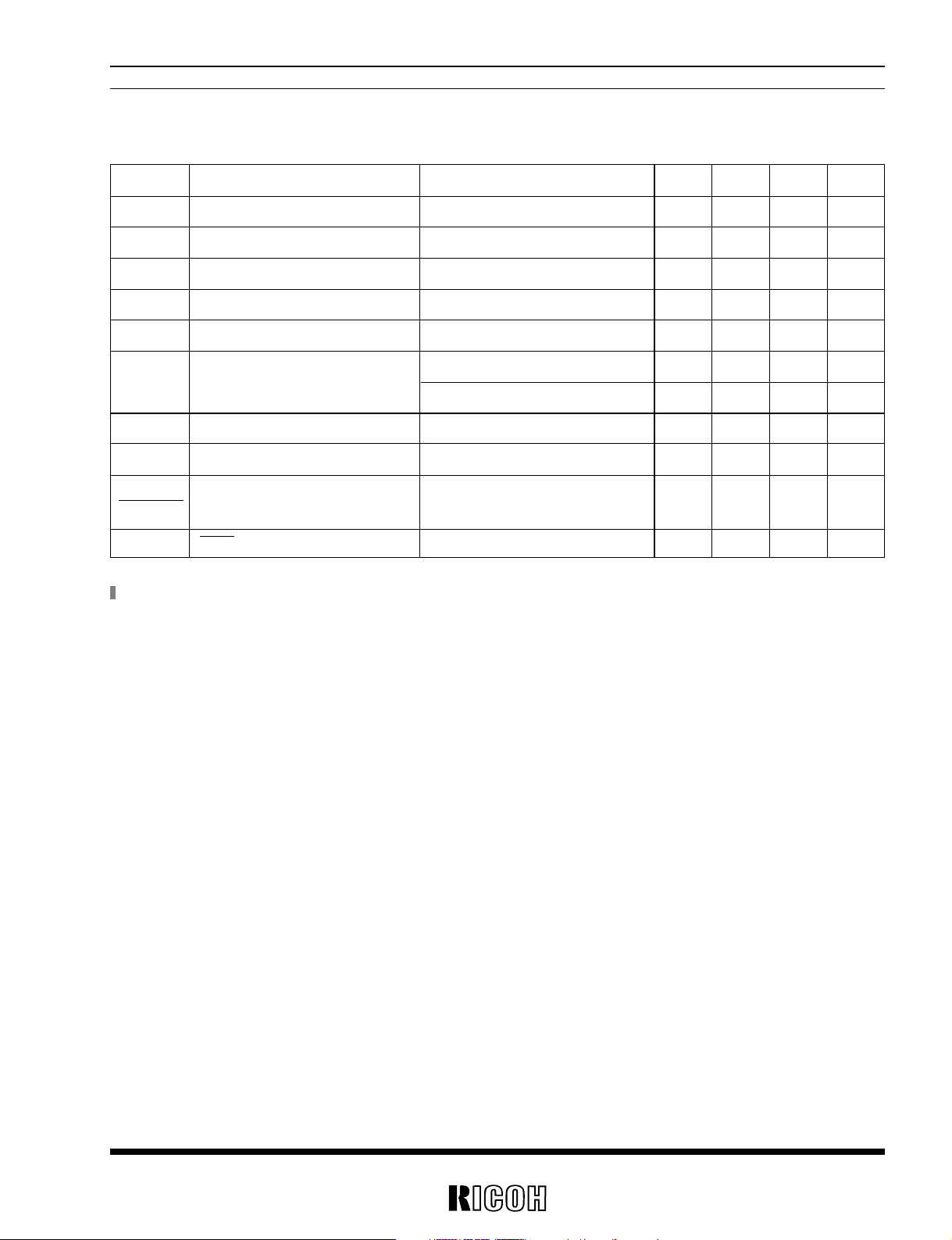
Symbol Item Conditions MIN. TYP. MAX. Unit
VOUT1 Step-up Output Voltage 4.875 5.000 5.125 V
VINmax Maximum Input Voltage 10 V
Vstart Oscillator Start-up Voltage No Load 0.7 0.8 V
Vhold Hold-on Input Voltage IOUT=1mA, VIN :2→0V 1.2 V
ISS1 Supply Current1 *
1
No Load, CSW=“L” 15 µA
ILX LX Switching Current VLX=0.4V 100 mA
ILXleak LX Leakage Current VLX=6.0V, VIN=5.5V 0.03 1 µA
fosc Maximum Oscillator Frequency 110 130 150 kHz
Maxdty Oscillator Duty Cycle ON (VLX=“L”) 55 70 85 %
η Efficiency 80 %
VLXlim Voltage Limit for LX Switch 0.4 0.8 V
∆V
OUT1
Output Voltage Temp. Coefficient –40˚C≤Topt≤85˚C ±100 ppm/˚C
∆Topt
RV5VH1××/RV5VH2××
10
DC/DC Converter 2
VOUT1=5.0V, Topt=25˚C
Symbol Item Conditions MIN. TYP. MAX. Unit
VSET Set Output Voltage *
1
–3.000 0 V
VFB Feed Back Voltage 0 mV
VIN Maximum Input Voltage 10 V
VOPTmin Minimum Operating Voltage IOUT=1mA 1.8 V
ISS2 Supply Current2 CSW= “H” at No Load 25 µA
Istandby Standby Current CSW=“L” 0.3 µA
IEXT2H EXT2 “H” Output Current VEXT2=VOUT1–0.4V 3 6 mA
IEXT2L EXT2 “L” Output Current VEXT2=0.4V 7 14 mA
fosc Maximum Oscillator Frequency 110 130 150 kHz
Maxdty Oscillator Duty Cycle VEXT2=“H” 40 50 60 %
VCSWH CSW “H” Input Voltage VOUT1=5.0V 1.6 VOUT1 V
VCSWL CSW “L” Input Voltage VOUT1=5.0V 0 0.4 V
ICSWleak CSW Input Leakage Current VOUT1=5.0V –0.5 0.5 µA
∆V
FB
Feed Back Voltage Temp.Coefficient –40˚C≤Topt≤85˚C ±30 µV/˚C
∆Topt
*
) VOUT1=3.0V, IOUT=1mA, Topt=25˚C, unless otherwise specified. (See Typical Application)
*
1 ) Adjustable by external resistors to -30V.
11
RV5VH1××/RV5VH2××
Voltage Detector
VOUT1=5.0V, Topt=25˚C
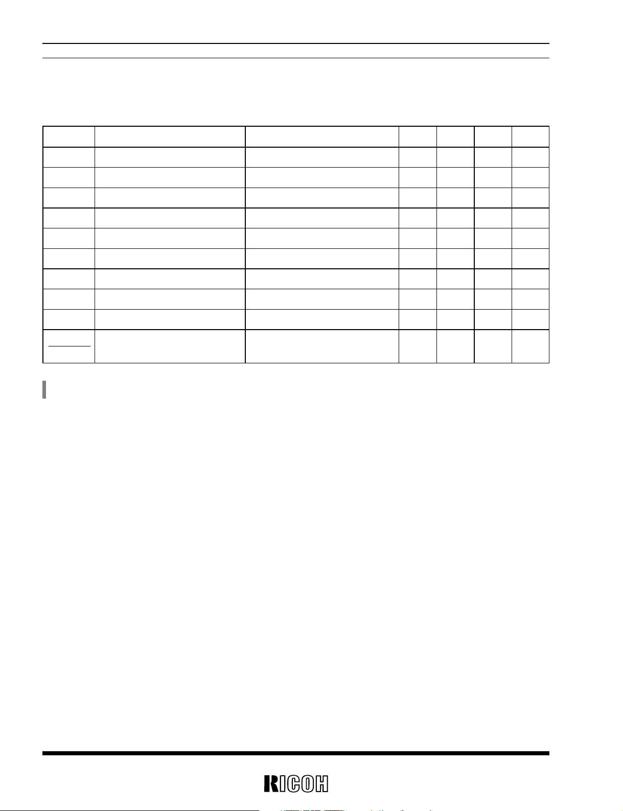
Symbol Item Conditions MIN. TYP. MAX. Unit
VDET Detector Threshold 4.388 4.500 4.612 V
VHYS Detector Threshold Hysteresis 0.135 0.225 0.315 V
ISS3 Supply Current3*
1
1.8 µA
VINmax Maximum Input Voltage 10 V
VOPTmin Minimum Operating Voltage*
2
1.8 V
IOUT Output Current
V
DS=0.5V, VOUT1=1.5V 1.0 2.0 mA
VDS=0.5V, VOUT1=5.0V 7.0 10.0 mA
ISEN Sensing Pin Input Current VSEN=5.0V 0.7 2.0 µA
tPLH Output Delay 100 µs
∆V
OUT1
DetectorThreshold Temp.Coefficient –40˚C≤Topt≤85˚C ±100 ppm/˚C
∆Topt
I
DOUTleak DOUT Leakage Current 0.03 0.5 µA
*
) VOUT1=3.0V, Topt=25˚C, unless otherwise specified. (See Typical Application)
RV5VH1××/RV5VH2××
12
Symbol Item Conditions MIN. TYP. MAX. Unit
VOUT1 Step-up Output Voltage IOUT=0mA 2.925 3.000 3.075 V
VINmax Maximum Input Voltage 10 V
Vstart Oscillator Start-up Voltage No Load 0.7 0.8 V
Vhold Hold-on Input Voltage IOUT=1mA 0.7 V
ISS1 Supply Current1 *
1
IOUT=0mA, CSW=“L” 80 µA
IEXT1H EXT1 “H” Output Current VEXT2=VOUT1–0.4V 1.5 3 mA
IEXT1L EXT1 “L” Output Current VEXT2=0.4V 4 8 mA
fosc Maximum Oscillator Frequency 110 130 150 kHz
Maxdty Oscillator Duty Cycle ON (VLX=“L”) 50 65 80 %
∆V
OUT1
Output Voltage Temp. Coefficient –40˚C≤Topt≤85˚C ±100 ppm/˚C
∆Topt
• RV5VH201
DC/DC Converter 1
VOUT1=3.0V, Topt=25˚C
*
) VIN=1.2V, IOUT=10mA, unless otherwise specified. (See Typical Application)
*
1 ) This value shows only the supply current of DC/DC1, not include the supply current of Voltage Detector and external resistors.

13
RV5VH1××/RV5VH2××
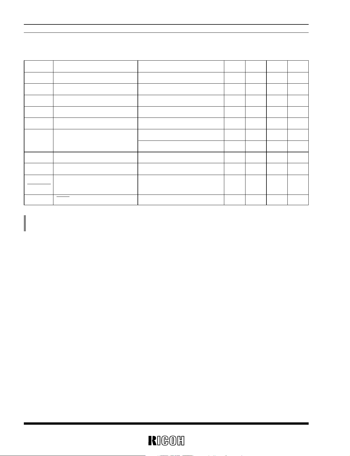
Symbol Item Conditions MIN. TYP. MAX. Unit
VSET Output Voltage Setting Range *
1
0V
VFB Feed Back Voltage –20 0 20 mV
VIN Maximum Input Voltage 10 V
VOPTmin Minimum Operating Voltage*
2
IOUT=1mA 1.8 V
ISS2 Supply Current2*
3
CSW= “H” IOUT=0mA 10 µA
Istandby Standby Current CSW=“L” 0.3 µA
IEXT2H EXT2 “H” Output Current VEXT2=VOUT1–0.4V 2 4 mA
IEXT2L EXT2 “L” Output Current VEXT2=0.4V 4 8 mA
fosc Maximum Oscillator Frequency 110 130 150 kHz
Maxdty Oscillator Duty Cycle VEXT2=“H” 40 50 60 %
VCSWH CSW “H” Input Voltage VOUT1=3.0V 1.6 VOUT1 V
VCSWL CSW “L” Input Voltage VOUT1=3.0V 0 0.4 V
ICSWleak CSW Input Leakage Current CSW=3.0V –0.5 0.5 µA
∆V
FB
Feed Back VoltageTemp. Coefficient –40˚C≤Topt≤85˚C ±30 µV/˚C
∆Topt
DC/DC Converter 2
*
) VOUT1=3.0V, VOUT2=-0.3V, IOUT2=1mA, unless otherwise specified. (See Typical Application)
*
1 ) Adjustable by external resistors to -30V.
*
2 ) “Minimum Operating Voltage”means a voltage for the “VOUT1” pin.
*
3 ) This value shows only the supply current of DC/DC2, not include the supply current of external resistors.
VOUT1=3.0V, Topt=25˚C
RV5VH1××/RV5VH2××
14
Voltage Detector
VOUT1=3.0V, Topt=25˚C
Symbol Item Conditions MIN. TYP. MAX. Unit
VDET Detector Threshold 2.633 2.700 2.767 V
VHYS Detector Threshold Hysteresis 0.081 0.135 0.189 V
ISS3 Supply Current3*
1
1.2 µA
VINmax Maximum Input Voltage 10 V
VOPTmin Minimum Operating Voltage*
2
1.8 V
IOUT Output Current
V
DS=0.5V, VOUT1=1.5V 1.0 2.0 mA
VDS=0.5V, VOUT1=3.0V 4.0 5.0 mA
ISEN Sensing Pin Input Current VSEN=3.0V 0.3 1.2 µA
tPLH Output Delay 100 µs
∆V
OUT1
DetectorThreshold Temp.Coefficient –40˚C≤Topt≤85˚C ±100 ppm/˚C
∆Topt
I
DOUTleak DOUT Leakage Current 0.03 0.5 µA
*
) VOUT1=3.0V : unless otherwise specified. (See Typical Application)
*
1 ) This value only shows the supply current of voltage detector.
*
2 ) “Minimum Operating Voltage”means a voltage for the “VOUT1” pin.
 Loading...