

Page 1

APPLICATION MANUAL
DC/DC CONVERTER
CONTROLLER
RV5VH SERIES
NO. EA-049-9803
ELECTRONIC DEVICES DIVISION
Page 2

NOTICE
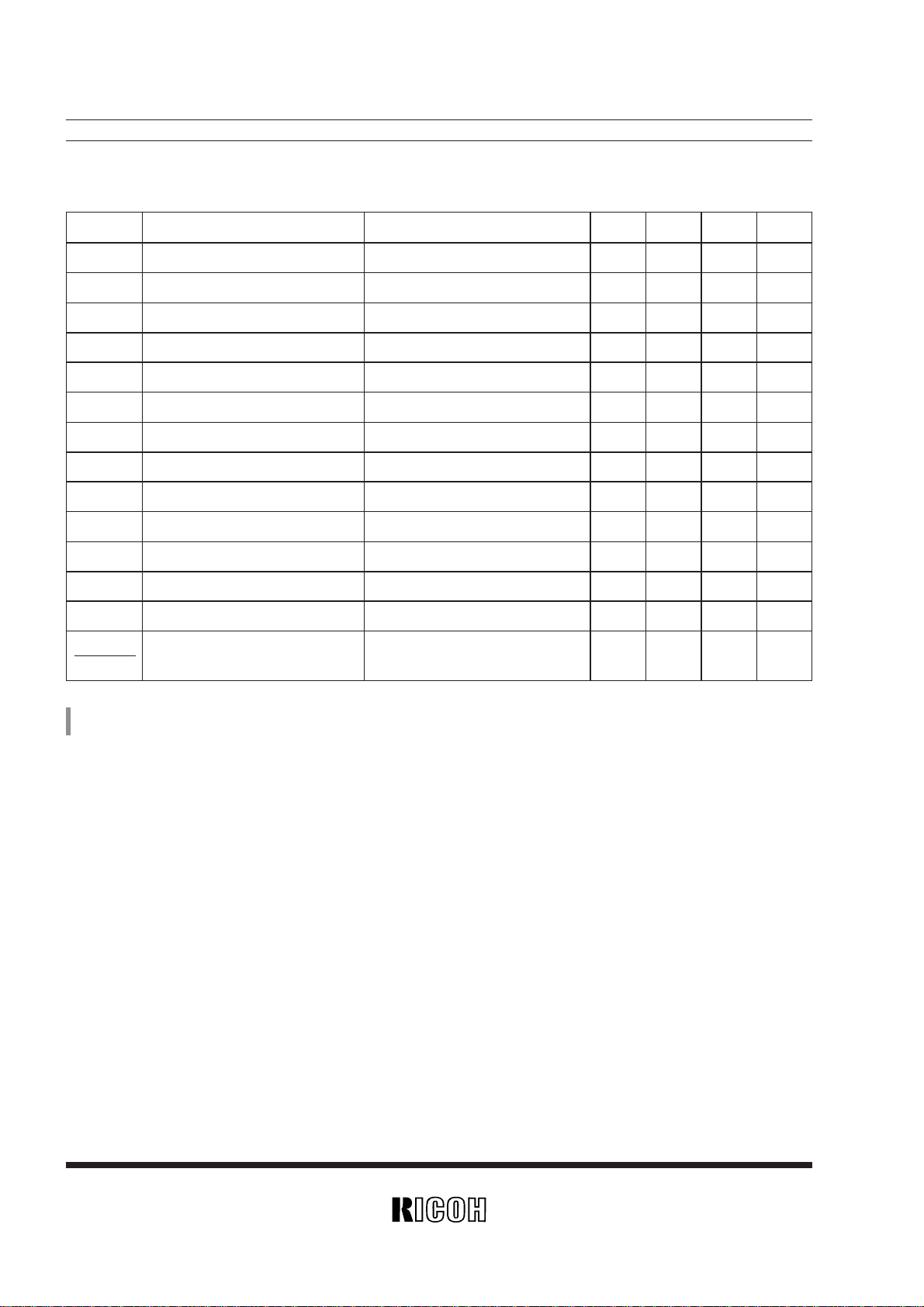
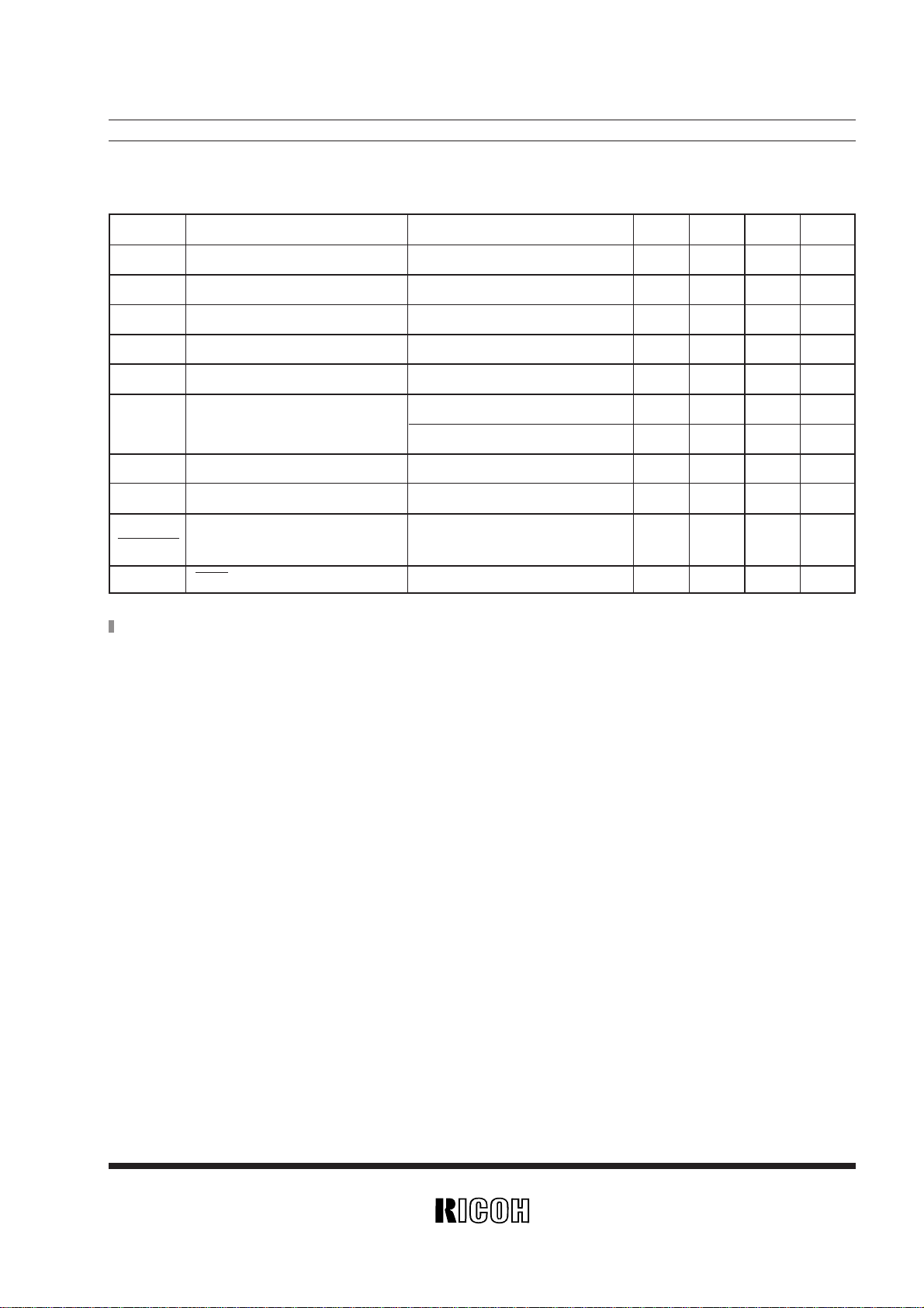
1. The products and the product specifications described in this application manual are subject to change or
discontinuation of production without notice for reasons such as improvement. Therefore, before deciding to
use the products, please refer to Ricoh sales representatives for the latest information thereon.
2. This application manual may not be copied or otherwise reproduced in whole or in part without prior written
consent of Ricoh.
3. Please be sure to take any necessary formalities under relevant laws or regulations before exporting or
otherwise taking out of your country the products or the technical information described herein.
4. The technical information described in this application manual shows typical characteristics of and example
application circuits for the products. The release of such information is not to be construed as a warranty of or a
grant of license under Ricoh's or any third party's intellectual property rights or any other rights.
5. The products listed in this document are intended and designed for use as general electronic components in
standard applications (office equipment, computer equipment, measuring instruments, consumer electronic
products, amusement equipment etc.). Those customers intending to use a product in an application requiring
extreme quality and reliability, for example, in a highly specific application where the failure or misoperation of
the product could result in human injury or death (aircraft, spacevehicle, nuclear reactor control system, traffic
control system, automotive and transportation equipment, combustion equipment, safety devices, life support
system etc.) should first contact us.
6. We are making our continuous effort to improve the quality and reliability of our products, but semiconductor
products are likely to fail with certain probability. In order prevent any injury to persons or damages to property
resulting from such failure, customers should be careful enough to incorporate safety measures in their design,
such as redundancy feature, fire-containment feature and fail-safe feature. We do not assume any liability or
responsibility for any loss or damage arising from misuse or inappropriate use of the products.
7. Anti-radiation design is not implemented in the products described in this application manual.
8. Please contact Ricoh sales representatives should you have any questions or comments concerning the
products or the technical information.
June 1995
Page 3

RV5VH SERIES
APPLICATION MANUAL
CONTENTS
OUTLINE
......................................................................................................
1
FEATURES
...................................................................................................
1
APPLICATIONS
.............................................................................................
1
RV5VH1
××
/RV5VH2
××
BLOCK DIAGRAMS
...................................................................................
2
PIN CONFIGURATION
................................................................................
3
PIN DESCRIPTION
....................................................................................
3
ABSOLUTE MAXIMUM RATINGS
...............................................................
4
ELECTRICAL CHARACTERISTICS
.............................................................
6
OPERATION
............................................................................................
18
OPERATION OF STEP-UP DC/DC CONVERTER
........................................
21
SELECTION OF PERIPHERAL COMPONENTS
.........................................
22
TYPICAL APPLICATION
...........................................................................
23
TEST CIRCUITS
.......................................................................................
24
TYPICAL CHARACTERISTICS
..................................................................
26
• DC/DC Converter 1
1) Output Voltage vs. Output Current (RV5VH1
××)
...............................................
26
2) Output Voltage vs. Output Current (RV5VH2××)
...............................................
26
3) Efficiency vs. Output Current (RV5VH1××)
......................................................
27
4) Efficiency vs. Output Current (RV5VH2××)
......................................................
27
5) DC/DC1 Output Voltage vs. Temperature
........................................................
28
6) Oscillator Frequency vs. Temperature
............................................................
28
7) Oscillator Duty Cycle vs. Temperature
...........................................................
28
8) On Resistance of LX vs. Supply Voltage
.........................................................
29
9) EXT1 Output Current vs. Temperature
...........................................................
29
10) Start-up/Hold-on Voltage vs. Output Current
....................................................
29
11) Input Current vs. Intput Voltage
...................................................................
29
• DC/DC Converter 2
12) Output Voltage vs. Output Current
................................................................
30
Page 4

13) DC/DC2 Feed Back Voltage vs. Temperature
...................................................
30
14) EXT2 Output Current vs. Temperature
...........................................................
30
15) EXT2 Oscillator Frequency vs. Temperature
....................................................
31
16) EXT2 Oscillator Duty Cycle vs. Temperature
....................................................
31
17) CSW ON/OFF Voltage vs. Temperature
........................................................
31
• Voltage Detector
18) Detector Threshold Voltage vs. Temperature
...................................................
32
19) VOUT1 Output Voltage vs. Output Current
........................................................
32
20) DOUT Output Current vs. VOUT1 Output Voltage
...............................................
32
21) VSEN Output Current vs. VSEN Output Voltage
................................................
32
22) Output Delay Time vs. Load Capacitance
.......................................................
32
RV5VH3
××
BLOCK DIAGRAMS
.................................................................................
33
PIN CONFIGURATION
..............................................................................
33
PIN DESCRIPTION
...................................................................................
34
ABSOLUTE MAXIMUM RATINGS
.............................................................
34
ELECTRICAL CHARACTERISTICS
...........................................................
35
OPERATION
............................................................................................
38
TYPICAL APPLICATION1
.........................................................................
41
TYPICAL APPLICATION2
.........................................................................
42
TYPICAL APPLICATION3
.........................................................................
43
TYPICAL CHARACTERISTICS
..................................................................
44
1) Output Voltage vs. Output Current
................................................................
44
2) Efficiency vs. Output Current
......................................................................
44
3) CSW Load Transient Responce 1
................................................................
44
4) CSW Load Transient Responce 2
................................................................
44
SELECTION GUIDE
.....................................................................................
45
PACKAGE DIMENSION
................................................................................
46
TAPING SPECIFICATION
.............................................................................
46
Page 5

1
DC/DC CONVERTER CONTROLLER
RV5VH SERIES
OUTLINE
The RV5VH series are dual output CMOS DC/DC converter ICs integrating Step-up and inverting DC/DC converters.
The RV5VH3
×× series ICs consist of an oscillator, two VFM control circuits, control transistors(EXT switches), a phase
shift circuit, a voltage reference unit, an error amplifier, and voltage sensing resistors. The RV5VH series are housed in 8pin
SSOP(0.65mm pitch) and suitable for two supply systems such as pager, PDA, which need power supplies for LCD.
RV5VH1
×× and RV5VH2×× series are able to provide two DC/DC converter systems, one system is step-up converter
with internally fixed output and another is inverting converter system with user adjustable output by external resistors. A
voltage detector with sensing pin is also included. RV5VH3
×× series are able to provide two DC/DC converter systems,
both of boost converter, DC/DC1, and inverting one, DC/DC2, can operate with external transistors being adjustable output by resistors. Further more reset output is available.
FEATURES
• Dual DC/DC converter system
.................................
DC/DC1 : step-up
DC/DC2 : inverting(negative voltage)
• Voltage Detector
..........................................................
Nch. Open Drain Output
• Low voltage operation available
RV5VH1
××,RV5VH2××
..........................................
oscillator start-up from 0.8V
RV5VH3
××
.................................................................
oscillator start-up from 1.8V
• High Efficiency
.............................................................
TYP. 80%
• Low Supply Current
• High accuracy feedback sensing
...............................
TYP. ±2.5%
• Sleep Mode
RV5VH1
××, RV5VH2××
..........................................
DC/DC 2
RV5VH3
××
.................................................................
DC/DC1, 2
• Available to adjust temperature drift
.........................
DC/DC2 : with external resistor (RV5VH2
××, RV5VH3××)
coefficient of output voltage
• Small Package
..............................................................
8pin SSOP(0.65mm pitch)
APPLICATIONS
• Power source for telecommunication system
• Power source for portable data processing system, e.g. PDA, Electronic Data Banks
• Power source for Audio-Visual system, e.g. CD player, Video camera
• Power source for Notebook PC, Word processing system
• Gadget being needed two power supplies, e.g. CPU and LCD
Page 6
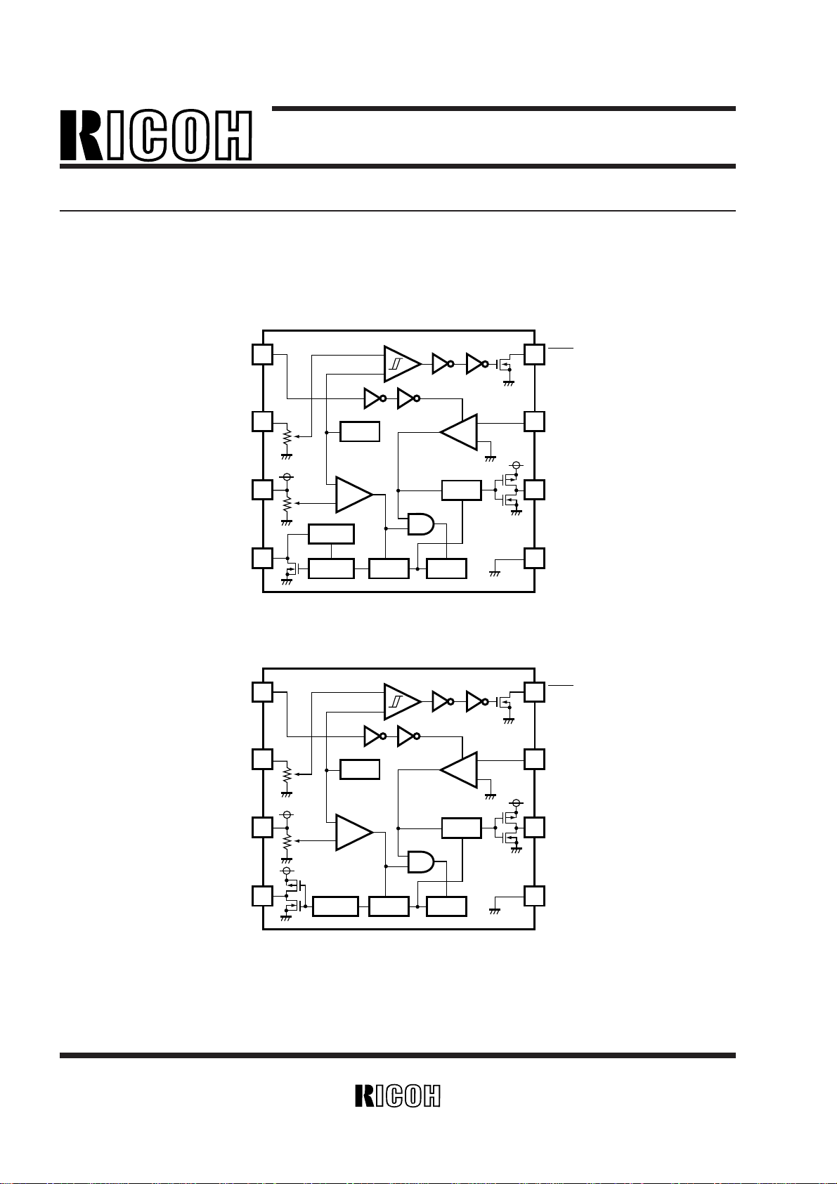
2
BLOCK DIAGRAM
+
–
+
–
CSW
V
SEN
VOUT1
LX1
DOUT
FB
EXT2
GND
Vref
Error Amp.1
Error Amp.2
1
2
3
4
8
7
6
5
VFM2
V
LX lim.
VFM1 OSC
p_shift
+
–
DC/DC CONVERTER CONTROLLER
(BOOST / INVERTING)
RV5VH1××/ RV5VH2××
+
–
+
–
CSW
V
SEN
VOUT1
EXT1
D
OUT
FB
EXT2
GND
Vref
Error Amp.1
Error Amp.2
1
2
3
4
8
7
6
5
VFM2
VFM1 OSC
p_shift
+
–
Page 7
3
RV5VH1××/RV5VH2××
PIN CONFIGURATION
1
2
3
4
8
7
6
5
• 8 pin SSOP (0.65mm pitch)
PIN DESCRIPTION
• RV5VH1××
Pin No. Symbol Description
1 CSW Control switch for DC/DC2
2 VSEN Sensing Pin for Voltage Detector
3 VOUT1 Output for DC/DC1, Power supply for the device
4 LX1 Output for DC/DC1, switching (Nch Open-Drain)
5 GND Ground
6 EXT2 External Transistor drive pin for DC/DC2 (CMOS output)
7 FB Input for DC/DC2 Error Amplifier
8 D
OUT Output for Voltage detector
• RV5VH2××
Pin No. Symbol Description
1 CSW Contol switch for DC/DC2
2 VSEN Sensing Pin for Voltage Detector
3 VOUT1 Output for DC/DC1, Power supply for the device
4 EXT1 External Transistor drive pin for DC/DC1 (CMOS output)
5 GND Ground
6 EXT2 External Transistor drive pin for DC/DC2 (CMOS output)
7 FB Input for DC/DC2 Error Amplifier
8 D
OUT Output for Voltage Detector
Page 8
RV5VH1××/RV5VH2××
4
ABSOLUTE MAXIMUM RATINGS
• RV5VH1××
Symbol Item Ratings Unit
VOUT1 VOUT1 Pin Voltage 12 V
VLX1 LX1 Pin Voltage 12 V
VSEN VSEN Pin Voltage 12 V
DOUT DOUT Pin Voltage 12 V
VCSW CSW Pin Voltage –0.3 to VOUT1 +0.3 V
VEXT2 EXT2 Pin Voltage –0.3 to VOUT1 +0.3 V
VFB FB Pin Voltage –0.3 to VOUT1 +0.3 V
ILX1 LX1 Output Current 400 mA
IEXT2 EXT2 Output Current ±50 mA
PD Power Dissipation 300 mW
Topt Operating Temperature –40 to +85 ˚C
Tstg Storage Temperature –55 to +125 ˚C
Tsolder Lead Temperature (Soldering) 260˚C 10sec
Page 9
5
RV5VH1××/RV5VH2××
ABSOLUTE MAXIMUM RATINGS
Absolute Maximum ratings are threshold limit values that must not be exceeded even for an instant under
any conditions. Moreover, such values for any two items must not be reached simultaneously. Operation
above these absolute maximum ratings may cause degradation or permanent damage to the device. These
are stress ratings only and do not necessarily imply functional operation below these limits.
• RV5VH2××
Symbol Item Ratings Unit
VOUT1 VOUT1 Pin Voltage 12 V
VSEN VSEN Pin Voltage 12 V
DOUT DOUT Pin Voltage 12 V
VCSW CSW Pin Voltage –0.3 to VOUT1 +0.3 V
VEXT1, 2 EXT1, 2 Pin Voltage –0.3 to VOUT1 +0.3 V
VFB FB Pin Voltage –0.3 to VOUT1 +0.3 V
IEXT1, 2 EXT1, 2 Output Current ±50 mA
PD Power Dissipation 300 mW
Topt Operating Temperature –40 to +85 ˚C
Tstg Storage Temperature –55 to +125 ˚C
Tsolder Lead Temperature (Soldering) 260˚C 10sec
Page 10
RV5VH1××/RV5VH2××
6
ELECTRICAL CHARACTERISTICS
• RV5VH101
DC/DC Converter 1
*
) VIN=1.2V, IOUT=10mA, Topt=25˚C, unless otherwise specified. (See Typical Application)
*
1 ) This value only shows the supply current of DC/DC1, not include the supply current of Voltage Detector and external resistors.
Symbol Item Conditions MIN. TYP. MAX. Unit
VOUT1 Step-up Output Voltage 2.925 3.000 3.075 V
VINmax Maximum Input Voltage 10 V
Vstart Oscillator Start-up Voltage No Load 0.7 0.8 V
Vhold Hold-on Input Voltage IOUT=1mA, VIN : 2→0V 0.7 V
ISS1 Supply Current1 *
1
No Load, CSW=“L” 10 µA
ILX LX Switching Current VLX=0.4V 100 mA
ILXleak LX Leakage Current VLX=6.0V, VIN=3.5V 0.03 1 µA
fosc Maximum Oscillator Frequency 110 130 150 kHz
Maxdty Oscillator Duty Cycle ON (V
LX=“L”) 50 65 80 %
η Efficiency 80 %
VLXlim Voltage Limit for LX Switch for LX pin 0.4 0.8 V
∆V
OUT1
Output Voltage Temp. Co. –40˚C≤Topt≤85˚C ±100 ppm/˚C
∆Topt
VOUT1=3.0V, Topt=25˚C
Page 11
7
RV5VH1××/RV5VH2××
DC/DC Converter 2
Symbol Item Conditions MIN. TYP. MAX. Unit
VSET Set Output Voltage *
1
0 V
VFB Feed Back Voltage –20 0 20 mV
VIN
Maximum Input Voltage 10 V
VOPTmin Minimum Operating Voltage IOUT=1mA 1.8 V
ISS2 Supply Current2 CSW= “H” at No Load 10 µA
Istandby Standby Current CSW=“L” 0.3 µA
IEXT2H
EXT2 “H” Output Current VEXT2=VOUT1–0.4V 2 4 mA
IEXT2L EXT2 “L” Output Current VEXT2=0.4V 4 8 mA
fosc Maximum Oscillator Frequency 110 130 150 kHz
Maxdty Oscillator Duty Cycle V
EXT2=“H” 40 50 60 %
VCSWH CSW “H” Input Voltage VOUT1=3.0V 1.6 VOUT1 V
VCSWL CSW “L” Input Voltage VOUT1=3.0V 0 0.4 V
ICSWleak CSW Input Leakage Current VOUT1=3.0V –0.5 0.5 µA
∆V
FB
Feed Back Voltage Co.Temp. –40˚C≤Topt≤85˚C ±30 µV/˚C
∆Topt
*
) VOUT1=3.0V, IOUT=1mA, Topt=25˚C, unless otherwise specified. (See Typical Application)
*
1 ) Adjustable by external resistors to -30V.
VOUT1=3.0V, Topt=25˚C
Page 12
RV5VH1××/RV5VH2××
8
Symbol Item Conditions MIN. TYP. MAX. Unit
VDET Detector Threshold 2.633 2.700 2.767 V
VHYS Detector Threshold Hysteresis 0.081 0.135 0.189 V
ISS3 Supply Current3 1.2 µA
VINmax Maximum Input Voltage 10 V
VOPTmin Minimum Operating Voltage 1.8 V
IOUT Output Current
V
DS=0.5V, V
OUT1=1.5V 1.0 2.0 mA
VDS=0.5V, VOUT1=3.0V 4.0 5.0 mA
ISEN Sensing pin Input Current VSEN=3.0V 0.3 1.2 µA
V
SEN Sensing pin Input Voltage 0.7 10 V
tPLH Output Delay 100 µs
∆V
OUT1
Detector Threshold Temp.Co. –40˚C≤Topt≤85˚C ±100 ppm/˚C
∆Topt
I
DOUTleak DOUT Leakage Current 0.03 0.5 µA
VOUT1=3.0V, Topt=25˚C
Voltage Detector
*
) VOUT1=3.0V, Topt=25˚C, unless otherwise specified. (See Typical Application)
Page 13
9
RV5VH1××/RV5VH2××
• RV5VH102
DC/DC Converter 1
*
) VIN=1.2V, IOUT=10mA, Topt=25˚C, unless otherwise specified. (See Typical Application)
*
1 ) This value only shows the supply current of DC/DC1, not include the supply current of Voltage Detector and external resistors.
VOUT1=5.0V, Topt=25˚C
Symbol Item Conditions MIN. TYP. MAX. Unit
VOUT1 Step-up Output Voltage 4.875 5.000 5.125 V
VINmax Maximum Input Voltage 10 V
Vstart Oscillator Start-up Voltage No Load 0.7 0.8 V
Vhold Hold-on Input Voltage IOUT
=1mA, VIN : 2→0V 1.2 V
ISS1 Supply Current1 *
1
No Load, CSW=“L” 15 µA
ILX LX Switching Current VLX=0.4V 100 mA
ILXleak LX Leakage Current VLX=6.0V, VIN=5.5V 0.03 1 µA
fosc Maximum Oscillator Frequency 110 130 150 kHz
Maxdty Oscillator Duty Cycle ON (VLX=“L”) 55 70 85 %
η Efficiency 80 %
VLXlim Voltage Limit for L
X Switch 0.4 0.8 V
DV
OUT1
Output Voltage Temp. Co. –40˚C≤Topt≤85˚C ±100 ppm/˚C
DTopt
Page 14
RV5VH1××/RV5VH2××
10
DC/DC Converter 2
VOUT1=5.0V, Topt=25˚C
Symbol Item Conditions MIN. TYP. MAX. Unit
VSET Set Output Voltage *
1
–3.000 0 V
VFB Feed Back Voltage 0 mV
VIN Maximum Input Voltage 10 V
VOPTmin Minimum Operating Voltage IOUT=1mA 1.8 V
ISS2 Supply Current2 CSW= “H” at No Load 25 µA
Istandby Standby Current CSW=“L” 0.3 µA
IEXT2H EXT2 “H” Output Current VEXT2=VOUT1–0.4V 3 6 mA
IEXT2L EXT2 “L” Output Current VEXT2=0.4V 7 14 mA
fosc Maximum Oscillator Frequency 110 130 150 kHz
Maxdty Oscillator Duty Cycle VEXT2=“H” 40 50 60 %
VCSWH CSW “H” Input Voltage VOUT1=5.0V 1.6 VOUT1 V
VCSWL CSW “L” Input Voltage VOUT1=5.0V 0 0.4 V
ICSWleak CSW Input Leakage Current VOUT1=5.0V –0.5 0.5 µA
∆V
FB
Feed Back Voltage Co.Temp. –40˚C≤Topt≤85˚C ±30 µV/˚C
∆Topt
*
) VOUT1=3.0V, IOUT=1mA, Topt=25˚C, unless otherwise specified. (See Typical Application)
*
1 ) Adjustable by external resistors to -30V.
Page 15
11
RV5VH1××/RV5VH2××
Voltage Detector
VOUT1=5.0V, Topt=25˚C
Symbol Item Conditions MIN. TYP. MAX. Unit
VDET Detector Threshold 4.388 4.500 4.612 V
VHYS Detector Threshold Hysteresis 0.135 0.225 0.315 V
ISS3 Supply Current3*
1
1.8 µA
VINmax Maximum Input Voltage 10 V
VOPTmin Minimum Operating Voltage*
2
1.8 V
IOUT
Output Current
V
DS=0.5V, VOUT1=1.5V 1.0 2.0 mA
VDS=0.5V, VOUT1=5.0V 7.0 10.0 mA
ISEN Sensing Pin Input Current VSEN=5.0V 0.7 2.0 µA
tPLH Output Delay 100 µs
∆V
OUT1
Detector Threshold Temp.Co. –40˚C≤Topt≤85˚C ±100 ppm/˚C
∆Topt
I
DOUTleak DOUT Leakage Current 0.03 0.5 µA
*
) VOUT1=3.0V, Topt=25˚C, unless otherwise specified. (See Typical Application)
Page 16
RV5VH1××/RV5VH2××
12
Symbol Item Conditions MIN. TYP. MAX. Unit
VOUT1 Step-up Output Voltage IOUT=0mA 2.925 3.000 3.075 V
VINmax Maximum Input Voltage 10 V
Vstart Oscillator Start-up Voltage No Load 0.7 0.8 V
Vhold Hold-on Input Voltage IOUT=1mA 0.7 V
ISS1 Supply Current1 *
1
IOUT=0mA, CSW=“L” 80 µA
IEXT1H EXT1 “H” Output Current VEXT2=VOUT1–0.4V 1.5 3 mA
IEXT1L EXT1 “L” Output Current VEXT2=0.4V 4 8 mA
fosc Maximum Oscillator Frequency 110 130 150 kHz
Maxdty Oscillator Duty Cycle ON (VLX=“L”) 50 65 80 %
∆V
OUT1
Output Voltage Temp. Co. –40˚C≤Topt≤85˚C ±100 ppm/˚C
∆Topt
• RV5VH201
DC/DC Converter 1
VOUT1=3.0V, Topt=25˚C
*
) VIN=1.2V, IOUT=10mA, unless otherwise specified. (See Typical Application)
*
1 ) This value shows only the supply current of DC/DC1, not include the supply current of Voltage Detector and external resistors.
Page 17

13
RV5VH1××/RV5VH2××
Symbol Item Conditions MIN. TYP. MAX. Unit
VSET Output Voltage Setting Range *
1
0 V
VFB Feed Back Voltage –20 0 20 mV
VIN Maximum Input Voltage 10 V
VOPTmin Minimum Operating Voltage*
2
IOUT=1mA 1.8 V
ISS2 Supply Current2*
3
CSW= “H” IOUT=0mA 10 µA
Istandby Standby Current CSW=“L” 0.3 µA
IEXT2H EXT2 “H” Output Current VEXT2=VOUT1–0.4V 2 4 mA
IEXT2L EXT2 “L” Output Current VEXT2=0.4V 4 8 mA
fosc Maximum Oscillator Frequency 110 130 150 kHz
Maxdty Oscillator Duty Cycle VEXT2=“H” 40 50 60 %
VCSWH CSW “H” Input Voltage VOUT1=3.0V 1.6 VOUT1 V
VCSWL CSW “L” Input Voltage VOUT1=3.0V 0 0.4 V
ICSWleak CSW Input Leakage Current CSW=3.0V –0.5 0.5 µA
∆V
FB
Feed Back Voltage Temp. Co. –40˚C≤Topt≤85˚C ±30 µV/˚C
∆Topt
DC/DC Converter 2
*
) VOUT1=3.0V, VOUT2=-0.3V, IOUT2=1mA, unless otherwise specified. (See Typical Application)
*
1 ) Adjustable by external resistors to -30V.
*
2 ) “Minimum Operating Voltage”means a voltage for the “VOUT1” pin.
*
3 ) This value shows only the supply current of DC/DC2, not include the supply current of external resistors.
VOUT1=3.0V, Topt=25˚C
Page 18

RV5VH1××/RV5VH2××
14
Voltage Detector
VOUT1=3.0V, Topt=25˚C
Symbol Item Conditions MIN. TYP. MAX. Unit
VDET Detector Threshold 2.633 2.700 2.767 V
VHYS Detector Threshold Hysteresis 0.081 0.135 0.189 V
ISS3 Supply Current3*
1
1.2 µA
VINmax Maximum Input Voltage 10 V
VOPTmin Minimum Operating Voltage*
2
1.8 V
IOUT
Output Current
V
DS=0.5V, VOUT1=1.5V 1.0 2.0 mA
VDS=0.5V, VOUT1=3.0V 4.0 5.0 mA
ISEN Sensing Pin Input Current VSEN=3.0V 0.3 1.2 µA
tPLH Output Delay 100 µs
∆V
OUT1
Detector Threshold Temp. Co. –40˚C≤Topt≤85˚C ±100 ppm/˚C
∆Topt
I
DOUTleak DOUT Leakage Current 0.03 0.5 µA
*
) V
OUT1=3.0V : unless otherwise specified. (See Typical Application)
*
1 ) This value only shows the supply current of voltage detector.
*
2 ) “Minimum Operating Voltage”means a voltage for the “VOUT1” pin.
Page 19

15
RV5VH1××/RV5VH2××
• RV5VH202
DC/DC Converter 1
VOUT1=5.0V, Topt=25˚C
*
) VIN=3.0V, IOUT=10mA : unless otherwise specified. (See Typical Application)
*
1 ) This value only shows the supply current of DC/DC1, does not include the supply current of Voltage Detector and external resistors.
Symbol Item Conditions MIN. TYP. MAX. Unit
VOUT1 Step-up Output Voltage IOUT=0mA 4.875 5.000 5.125 V
VINmax Maximum Input Voltage 10 V
Vstart Oscillator Start-up Voltage No Load 0.7 0.8 V
Vhold Hold-on Input Voltage IOUT=1mA 0.7 V
ISS1 Supply Current1 *
1
IOUT=0mA, CSW=“L” 40 µA
IEXT1H EXT1 “H” Output Current VEXT2=VOUT1–0.4V 2 4 mA
IEXT1L EXT1 “L” Output Current VEXT2=0.4V 7 14 mA
fosc Maximum Oscillator Frequency 110 130 150 kHz
Maxdty Oscillator Duty Cycle ON (VLX=“L”) 55 70 85 %
η Efficiency 80 %
∆V
OUT1
Output Voltage Temp. Co. –40˚C≤Topt≤85˚C ±100 ppm/˚C
∆Topt
Page 20

RV5VH1××/RV5VH2××
16
DC/DC Converter 2
*
) VOUT1=5.0V, VOUT2=–3.0V, IOUT2=1mA : unless otherwise specified. (See Typical Application)
*
1 ) Adjustable by external resistors to -30V.
*
2 ) “Minimum Operating Voltage”means a voltage for the “VOUT1” pin.
*
3 ) This value shows only the supply current of DC/DC2, not include the supply current of external resistors.
Symbol Item Conditions MIN. TYP. MAX. Unit
VSET Output Voltage Setting Range *
1
0 V
VFB Feed Back Voltage 0 mV
VIN Maximum Input Voltage 10 V
VOPTmin Minimum Operating Voltage*
2
IOUT=1mA 1.8 V
ISS2 Supply Current2*
3
CSW= “H”, No Load 25 µA
Istandby Standby Current CSW=“L” 0.3 µA
IEXT2H EXT2 “H” Output Current VEXT2=VOUT1–0.4V 3 6 mA
IEXT2L EXT2 “L” Output Current VEXT2=0.4V 7 14 mA
fosc Maximum Oscillator Frequency 110 130 150 kHz
Maxdty Oscillator Duty Cycle VEXT2=“H” 40 50 60 %
VCSWH CSW “H” Input Voltage VOUT1=5.0V 1.6 VOUT1 V
VCSWL CSW “L” Input Voltage VOUT1=5.0V 0 0.4 V
ICSWleak CSW Input Leakage Current CSW=5.0V –0.5 0.5 µA
∆V
FB
Feed Back Voltage Temp.Co. –40˚C≤Topt≤85˚C ±30 µV/˚C
∆Topt
VOUT1=5.0V, Topt=25˚C
Page 21

17
RV5VH1××/RV5VH2××
Voltage Detector
VOUT1=5.0V, Topt=25˚C
*
) V
OUT1=5.0V : unless otherwise specified. (See Typical Application)
*
1 ) This value only shows the supply current of voltage detector.
*
2 ) “Minimum Operating Voltage”means a voltage for the “VOUT1” pin.
Symbol Item Conditions MIN. TYP. MAX. Unit
VDET Detector Threshold 4.388 4.500 4.612 V
VHYS Detector Threshold Hysteresis 0.135 0.225 0.315 V
ISS3 Supply Current3*
1
1.8 µA
VINmax Maximum Input Voltage 10 V
VOPTmin Minimum Operating Voltage*
2
1.8 V
IOUT
Output Current
V
DS=0.5V, VOUT1=1.5V 1.0 2.0 mA
VDS=0.5V, VOUT1=5.0V 7.0 10.0 mA
ISEN Sensing Pin Input Current VSEN=5.0V 0.7 2.0 µA
tPLH Output Delay 100 µs
∆V
OUT1
Detector Threshold Temp.Co. –40˚C≤Topt≤85˚C ±100 ppm/˚C
∆Topt
I
DOUTleak DOUT Leakage Current 0.03 0.5 µA
Page 22

RV5VH1××/RV5VH2××
18
OPERATION
• DC/DC Converter 1
The DC/DC1 uses input voltage as an initial power supply, once boost operation is started the boost output will be used for
the power supply of device itself. A change in the V
OUT1 will feed back to the internal error amplifier through external volt-
age setting resistors and internal feed back resistors. When the feed back voltage is lower than the reference voltage the
error amplifier enables oscllation or otherwise will stop oscillation. The internal feed back resistor “R” which is fixed and
adjusted by laser trim can make the feed back input voltage to “Error Amp.1” stable. Pulses from the “OSC” circuit have a
duty cycle of 50% and it becomes 65 to 75%(at high side) through the “P_shift” circuit. The duty cycle may be smaller in a
short period of time with light load.
These clook pulses control VFM circuit and make it possible to operate as a boost converter. The output of L
X1 is Nch open
drain, while the output of “EXT1” is driven by CMOS buffer and an external NMOS driver is also available instead of an
NPN transistor, in such cases the Rb and Cb are not necessary, a recommended Rb is 300Ω. When you use a MOSFET
for the EXT1, the input voltage should be high enough and you can get high effiiciency applications.
A current limit is available only for the RV5VH1 series, to prevent an excess current from flowing through Nch driver transistor.
The DC/DC1 can be shut down by CSW pin. When the CSW pin is High, V
DD level, the DC/DC1 is enabled and when the
CSW pin is Low, GND level, the DC/DC1 is disabled. The EXT1 pin outputs “L” while the DC/DC1 is disabled.
C
L
SBD
V
OUT1
VOUT1
LX1
R
–
+
VLX lim.
OSC
Vref
p_shift
VFM1
VIN
RV5VH1××
Error Amp.1
3
4
C
L1
SBD
V
OUT1
VOUT1
EXT1
R
–
+
OSC
Vref
p_shift
V
IN
RV5VH2××
Error Amp.1
VFM1
NPN Tr.
Cb
3
4
Rb
Page 23

19
RV5VH1××/RV5VH2××
C1
L
FB
V
OUT2
VOUT1
EXT2
+
–
RV5VH1××/RV5VH2××
Error Amp.2
VFM2
CSW
6
1
7
SBD
+
PMOS
OSC
C2 R2
R1
The DC/DC2 can operate by a voltage of “VOUT1”. A change in the VOUT2 will feed back to the internal error amplifier
through external voltage setting resistors. The reference voltage should be provided from externally fixed power supply
such as V
OUT1.
When the feed back voltage to the cmp2 is higher than the ground voltage the error amplifier enables oscillation or otherwise will stop oscillation.
Pulses from the “OSC” circuit have a duty cycle of 50% and it makes VFM operation allowable. There might be certain cases that the duty cycles becomes smaller temporally at light load current. The output of “EXT2” is driven by CMOS buffer
operated V
OUT1 and GND.
A PMOS driver will be connected to the “EXT2” pin and its switching operation generates negative output voltage through
energy accumulated in an inductor.
The DC/DC1 can be shut down by CSW pin. When the CSW pin is High, V
DD level, the DC/DC1 is enabled and when the
CSW pin is Low, GND level, the DC/DC1 is disabled. The EXT2 pin outputs High while the DC/DC2 is disabled.
• Set output voltage DC/DC Converter2
V
OUT2 is described as follows:
V
OUT1:R1=|–VOUT2| : R2 / The FB voltage is controlled to 0V and VOUT1 is provided externally
|–V
OUT2|=VOUT1 × R2/R1
so any output voltage of DC/DC2 can be set by changing R1 or/and R2.
Certain temperature coefficient of V
OUT2 can be set by using R1,R2 having such temperature characteristics.
• DC/DC Converter 2
Page 24

RV5VH1××/RV5VH2××
20
VSEN
DOUT
RV5VH1××/RV5VH2××
Pull-up
Output Tr.
–
+
Vref
Ra
Rb
Rc
Tr.1
2
8
The VD can operate by the voltage of “VOUT1”. The detector threshold and the reset voltage are internally adjusted by
trimmed resistors and the VD monitors V
SEN pin voltage.
The D
OUT is Nch-opendrain output and a pull up resistor is necessary.
Oepration Diagram
V
SEN pin is pulled up to VOUT1 voltage
• Voltage Detector
A
B
Reset Voltage
Detector Threshold
GND
GND
Output Voltage
1 2 3 4 5
Hysteresis Range
+VDET
–V
DET
Step Step 1 Step 2 Step 3 Step 4 Step 5
Comparator(+) Pin
Input Voltage
A B B B A
Comparator Output
H L L L H
Tr. 1 OFF ON ON ON OFF
Output Tr
OFF ON
Indefinite
ON OFF
A :
Rb+Rc
×
VSEN
Ra+Rb+Rc
B :
Rb
×
V
SEN
Ra+Rb+Rc
Step 1. Output Voltage is equal to Pull-up Voltage.
Step 2. When Input voltage (V
SEN) reaches the state of Vref≥VSEN×(Rb×Rc)/(Ra+Rb+Rc) at point A, the output of the comparator is reversed. so that the
output voltage becomes to GND.
Step 3. Output VoItage becomes indefinite when Power source Voltage (V
SEN) is smaller than Minimum Operating VoItage. When the output is pulIed up,
Output becomes pull-up voltage and GND.
Step 4. Output VoItage becomes to GND.
Step 5. When input voltage(V
SEN) reaches the state of Vref≤VSEN×Rb/(Ra+Rb) at point B, the output of the comparator is reversed, so that the output voltage
becomes to pull-up voltage.
Page 25

21
RV5VH1××/RV5VH2××
OPERATION OF STEP-UP DC/DC CONVERTER
Step-up DC/DC Converter charges energy in the inductor when Lx Transistor (LxTr) is on, and discharges the
energy with the addition of the energy from Input Power Source thereto, so that a higher output voltage than the
input voltage is obtained.
The operation will be explained with reference to the following diagrams :
< Current through L >< Basic Circuits >
i2
L
SD
I
OUT
VOUT
CLLx Tr
i1
V
IN
IL
ILmin
ILmax
topen
t
ton
toff
T=1/fosc
Step 1 : LxTr is turned ON and current IL (=i1 ) flows, so that energy is charged in L. At this moment, IL(=i1 )
is increased from ILmin (=0) to reach ILmax in protection to the on-time period (ton) of LxTr.
Step 2 : When LxTr is turned OFF, Schottky diode (SD) is turned on in order that L maintains IL at ILmax, so that
current IL (=i2) is released.
Step 3 : IL (=i2) is gradually decreased, and IL reaches ILmin (=0) after a time period of topen, so that SD is
turned OFF.
In the case of VFM control system, the output voltage is maintained constant by controlling the oscillator fre-
quency (fosc) with the on-time period (ton) being maintained constant.
In the above two diagrams, the maximum value (ILmax) and the minimum value (ILmin) of the current which
flows through the inductor are the same as those when LxTr is ON and also when LxTr is OFF.
The difference between ILmax and ILmin, which is represented by ∆I, is:
∆I=ILmax–ILmin=V
IN · ton/L=(VOUT–VIN) · topen/L
..........................................
Equation 1
wherein T=1/fosc=ton+toff
duty (%)=ton/T · 100=ton · fosc · 100
topen≤toff
In Equation 1,V
IN · ton/L and (VOUT–VIN) · topen/L are respectively the change in the current at ON, and the
change in the current at OFF.
In the VFM system, topen < toff as illustrated in the above diagram. In this case, the energy charged in the
inductor during the time period of ton is discharged in its entirely during the time period of toff, so that ILmin
becomes zero (ILmin=0).
Page 26

RV5VH1××/RV5VH2××
22
The above explanation is directed to the calculation in an ideal case where it is supposed that there is no
energy loss in the external components and LxSW. In an actual case, the maximum output current will be 50
to 80% of the above calculated maximum output current. In particular, care must be taken because V
IN is
decreased in an amount corresponding to the voltage reduction caused by LxSW when IL is large or V
IN
is
small. Furthermore, It is required that with respect to V
OUT, Vf of the diode (about 0.3V in the case of a
Schottky type diode) be taken into consideration.
When I
LX and VLX exceed their respective ratings, use the RV5VH with the attachment of an external tran-
sistor with a low saturation voltage thereto.
HINTS
When LxTr is on, the energy PON charged in the inductor is provided by Equation 2 as follows :
P
ON=∫
0
ton
(VIN · IL (t)) dt=∫
0
ton
(VIN2· t/L) dt
=V
IN
2
· ton2/(2 · L)
....................................................................................................
Equation 2
In the case of the step-up DC/DC converter, the energy is also supplied from the input power source at the time
of OFF.
Thus, P
OFF = ∫
0
topen
(VIN · IL (t)) dt=∫
0
topen
(VIN · (VOUT–VIN) · t/L)dt
=V
IN · (VOUT–VIN) · topen
2
/(2 · L)
Here, topen=V
IN · ton/(VOUT–VIN) from Equation 1, and when this is substituted into the above equation.
=V
IN
3
· ton2/(2 · L · (VOUT–VIN))
............................................................................
Equation 3
Input power P
IN is (PON+POFF
)/T. When this is converted in its entirely to the output.
P
IN=(PON+POFF)/T=VOUT · IOUT=POUT
.........................................................................
Equation 4
Equation 5 can be obtained as follows by solving Equation 4 for I
OUT by substituting Equation 2 and 3 into
Equation 4 :
I
OUT=VIN
2
· ton2/(2 · L · T · (VOUT–VIN)
=V
IN
2
· maxdty2/(20000 · fosc · L · (VOUT –VIN))
...................................................
Equation 5
The peak current which flows through L · LxTr · SD is
ILmax=V
IN · ton/L
..........................................................................................................
Equation 6
Therefore, it is necessary that the setting of the input/output conditions and the selection of peripheral compo -
nents be made with ILmax taken into consideration.
SELECTION OF PERIPHERAL COMPONENTS
Page 27

23
RV5VH1××/RV5VH2××
<Components> Coils L1 : 27µH, L2 : 220µH
Diodes Schottky type
Capacitors C1 : 47µF(tantalum type), C2 : 22µF(tantalum type)
C3 : 0.01µF(ceramic type)
C4 : 0.01µF(ceramic type)
PMOS 2SJ238(TOSHIBA), etc.
NPN Tr. 2SD1628G(SANYO), etc.
Resistors R1 : 100KΩ
R2 : 0-500KΩ
R3 : 100KΩ
R4 : 300Ω
TYPICAL APPLICATION
• RV5VH1××
CSW
V
SEN
VOUT1
LX1
DOUT
FB
EXT2
GND
C2
L1
L2
D1
PMOS
R3
R1
R2 C3
D2
C1
Output DC/DC1
Output DC/DC2
• RV5VH2××
CSW
V
SEN
VOUT1
EXT1
D
OUT
FB
EXT2
GND
C2
L1
L2
SBD
PMOS
R3
R1
R2 C3
SBD
C1
NPN Tr.
C4
R4
Output DC/DC1
Output DC/DC2
<Components> CoiIs L1 : 100µH, L2 : 220µH
Diodes Schottky type
Capacitors C1, C2 : 22µF(tantalum type), C3 : 0.01µF(ceramic type)
Tr PMOS : 2SJ238
Resistors R1, R2 : several hundreds kΩ, R3 : 100kΩ
Page 28

RV5VH1××/RV5VH2××
24
TEST CIRCUITS
CSW DOUT
FB
EXT2
L1=100µH,220µH
GND
VSEN
VOUT1
LX1
L1
V
22µF
A
Fig.1 Test Circuit 1
CSW DOUT
FB
EXT2
GND
V
SEN
VOUT1
LX1(EXT1)
100kΩ
150Ω
A
VV
5Ω
(150Ω)
Oscilloscope
*
EXT1
*
Fig.2 Test Circuit 2
CSW DOUT
FB
EXT2
GND
V
SEN
VOUT1
LX1
A
0.5V
Fig.3 Test Circuit 3
Page 29

25
RV5VH1××/RV5VH2××
Test Circuit 1: Typical Characteristics 1), 3), 5), 10), 11)
Test Circuit 2: Typical Characteristics 6), 7), 8), 9), 13), 14), 15), 16), 17), 18), 19), 21)
Test Circuit 3: Typical Characteristics 20)
Test Circuit 4: Typical Characteristics 22)
Test Circuit 5: Typical Characteristics 2), 4)
Typical Application : Typical Characteristics 12)
CSW DOUT
FB
EXT2
GND
V
SEN
VOUT1
LX1
100kΩ
Pulse Input
Oscilloscope
Fig.4 Test Circuit 4
CSW DOUT
FB
EXT2
GND
V
SEN
VOUT1
EXT1
V
96µF 27µH
2200pF
300Ω
A
Fig.5 Test Circuit 5
Page 30

RV5VH1××/RV5VH2××
26
TYPICAL CHARACTERISTICS
• DC/DC Converter 1
1) Output Voltage vs. Output Current (RV5VH1
××)
RV5VH101
3.6
3.4
3.2
2.8
3.0
2.4
2.6
2.2
2.0
Output Current IOUT(mA)
Output Voltage VOUT1(V)
0 20 40 60 80 100 140120
VIN=0.9V
V
IN=1.2V
V
IN=1.5V VIN=2.0V
Topt=25˚C
L1=100µH
C1=22µF
RV5VH101
3.6
3.4
3.2
2.8
3.0
2.4
2.6
2.2
2.0
Output Current IOUT(mA)
Output Voltage VOUT1(V)
0 20 40 60 80 100 140120
Topt=25˚C
L1=220µH
C1=22µF
VIN=0.9V
V
IN=1.2V
V
IN=1.5V
V
IN=2.0V
RV5VH201
3.6
3.4
2.8
3.0
3.2
2.6
2.2
2.4
2.0
Output Current IOUT(mA)
Output Voltage VOUT(V)
0 100 200 300 400 500
Topt=25˚C
L1=27µH
C1=96µF
VIN=1.2V
VIN=0.9V
VIN=2.0V
VIN=1.5V
RV5VH202
6.0
5.5
4.5
5.0
4.0
3.5
3.0
Output Current IOUT(mA)
Output Voltage VOUT(V)
0 100 200 300 400 500
Topt=25˚C
L1=27µH
C1=96µF
VIN=0.9V
VIN=1.5V
VIN=4.0V
VIN=2.0V
VIN=3.0V
RV5VH102
6.0
5.5
4.5
5.0
4.0
3.5
3.0
Output Current IOUT(mA)
Output Voltage VOUT1(V)
0 50 100 150 200 250 300
Topt=25˚C
L1=100µH
C1=22µF
VIN=0.9V
V
IN=1.5V
V
IN=2.0V
VIN=4.0V
VIN=3.0V
RV5VH102
6.0
5.5
4.5
5.0
4.0
3.5
3.0
Output Current IOUT(mA)
Output Voltage VOUT1(V)
0 50 100 150 200 250 300
Topt=25˚C
L1=220µH
C1=22µF
VIN=0.9V
V
IN=1.5V
V
IN=2.0V
VIN=4.0V
VIN=3.0V
2) Output Voltage vs. Output Current (RV5VH2××)
Page 31

27
RV5VH1××/RV5VH2××
3) Efficiency vs. Output Current (RV5VH1××)
RV5VH101
100
75
80
85
90
95
65
70
55
60
50
Output Current IOUT(mA)
Efficiency η(%)
0.01 0.1 1 10 100
Topt=25˚C
L1=100µH
C1=22µF
VIN=0.9V
VIN=1.2V
VIN=2.0V
VIN=1.5V
RV5VH101
100
75
80
85
90
95
65
70
55
60
50
Output Current IOUT(mA)
Efficiency η(%)
0.01 0.1 1 10 100
Topt=25˚C
L1=220µH
C1=22µF
VIN=1.2V
VIN=2.0V
VIN=1.5V
VIN=0.9V
RV5VH102
100
75
80
85
90
95
65
70
55
60
50
Output Current IOUT(mA)
Efficiency η(%)
0.1 1 10 100 1000
Topt=25˚C
L1=100µH
C1=22µF
VIN=1.5V
VIN=0.9V
VIN=2.0V
VIN=3.0V
VIN=4.0V
RV5VH102
100
75
80
85
90
95
65
70
55
60
50
Output Current IOUT(mA)
Efficiency η(%)
0.1 1 10 100 1000
Topt=25˚C
L1=220µH
C1=22µF
VIN=1.5V
VIN=0.9V
VIN=2.0V
VIN=3.0V
VIN=4.0V
RV5VH201
90
65
70
75
80
85
55
60
45
50
40
Output Current IOUT(mA)
Efficiency η(%)
0.01 0.1 1 10 100 1000
Topt=25˚C
L1=27µH
C1=96µF
VIN=1.5V
VIN=0.9V
VIN=1.2V
VIN=2.0V
RV5VH202
90
65
70
75
80
85
55
60
45
50
40
Output Current IOUT(mA)
Efficiency η(%)
0.1 1 10 100 1000
Topt=25˚C
L1=27µH
C1=96µF
VIN=1.5V
VIN=0.9V
VIN=2.0V
VIN=3.0V
VIN=4.0V
4) Efficiency vs. Output Current (RV5VH2××)
Page 32

RV5VH1××/RV5VH2××
28
5) DC/DC1 Output Voltage vs. Temperature
RV5VH1××/2××
3.3
3.0
3.2
3.1
2.9
2.8
2.7
Temperature Topt(˚C)
Output Voltage VOUT(V)
–60 –40 –20 0 20 40 60 80 100
VIN=1.2V
L1=100µH
C1=22µF
IOUT=10mA
I
OUT=5mA
I
OUT=0A
RV5VH1××/2××
5.3
5.0
5.2
5.1
4.9
4.8
4.7
Temperature Topt(˚C)
Output Voltage VOUT(V)
–60 –40 –20 0 20 40 60 80 100
VIN=3V
L1=100µH
C1=22µF
IOUT=10mA
IOUT=0A
IOUT=1mA
RV5VH1××/2××
150
125
130
135
140
145
100
105
110
115
120
Temperature Topt(˚C)
Oscillator Frequency fosc(kHZ)
–60 –40 –20 0 20 40 60 80 100
VOUT1=3V
RV5VH1××/2××
150
125
130
135
140
145
100
105
110
115
120
Temperature Topt(˚C)
Oscillator Frequency fosc(kHZ)
–60 –40 –20 0 20 40 60 80 100
VOUT1=5V
RV5VH1××/2××
80
65
70
75
50
55
60
Temperature Topt(˚C)
Oscillator Duty Cycle Maxdty(%)
–60 –40 –20 0 20 40 60 80 100
VOUT1=3V
RV5VH1××/2××
80
65
70
75
50
55
60
Temperature Topt(˚C)
Oscillator Duty Cycle Maxdty(%)
–60 –40 –20 0 20 40 60 80 100
VOUT1=5V
7) Oscillator Duty Cycle vs. Temperature
6) Oscillator Frequency vs. Temperature
Page 33

29
RV5VH1××/RV5VH2××
8) On Resistance of LX vs. Supply Voltage
RV5VH1××
5.0
4.0
4.5
2.5
3.0
2.0
3.5
0.0
1.5
1.0
0.5
Supply Voltage VOUT1(V)
On Resistance Ron (Ω)
0.0 1.0 2.0 3.0 4.0 5.0 6.0
85˚C
25˚C
–40˚C
RV5VH201
18
12
10
8
16
14
0
6
4
2
Temperature Topt(˚C)
Output Current IOUT(mA)
–60 –40 –20 0 20 40 60 80 100
VOUT1=3V
“L” Output Current
“H” Output Current
RV5VH202
18
12
10
8
16
14
0
6
4
2
Temperature Topt(˚C)
Output Current IOUT(mA)
–60 –40 –20 0 20 40 60 80 100
VOUT1=5V
“L” Output Current
“H” Output Current
RV5VH1××/2××
2
1
1.2
1.4
1.6
1.8
0
0.2
0.4
0.6
0.8
Output Current IOUT(mA)
Start-up/Hold-on Voltage Vstart/Vhold(V)
0 20 30 4010 50
Topt=25˚C
V
OUT1=3V
L1=100µH
C1=22µF
Vstart
Vhold
RV5VH101
10
–0
10
–6
10
–5
10
–4
10
–3
10
–2
10
–1
Input Voltage VIN(V)
Input Current IIN(A)
0.0 1.0 1.5 2.0 2.50.5 3.0
Topt=25˚C
CSW=GND
L1=100µH
C1=22µF
IOUT=30mA
IOUT=5mA
IOUT=1mA
IOUT=0A
10) Start-up/Hold-on Voltage vs. Output Current
9) EXT1 Output Current vs. Temperature
11) Input Current vs. Intput Voltage
Page 34

RV5VH1××/RV5VH2××
30
12) Output Voltage vs. Output Current
RV5VH101
0
–2
–4
–6
–14
–10
–12
–8
Output Current IOUT(mA)
Output Voltage VOUT(V)
0 4 86 10 122 14
Topt=25˚C
VIN=1.2V
V
OUT1=3V
VSET –6V
VSET –9V
VSET –12V
V
SET –3V
RV5VH1××/2××
0.010
–0.010
–0.004
–0.002
0.000
0.002
0.004
0.006
0.008
–0.006
–0.008
Temperature Topt(˚C)
Feed Back Voltage VFB(V)
–60 –40 –20 0 20 40 60 80 100
RV5VH1××/2××
20
0
6
8
10
12
14
16
18
4
2
Temperature Topt(˚C)
Output Current IOUT(mA)
–60 –40 –20 0 20 40 60 80 100
VOUT1=3V
“L” Output Current
“H” Output Current
RV5VH1××/2××
20
0
6
8
10
12
14
16
18
4
2
Temperature Topt(˚C)
Output Current IOUT(mA)
–60 –40 –20 0 20 40 60 80 100
VOUT1=5V
“L” Output Current
“H” Output Current
14) EXT2 Output Current vs. Temperature
13) DC/DC2 Feed Back Voltage vs. Temperature
• DC/DC Converter 2
Page 35

31
RV5VH1××/RV5VH2××
15) EXT2 Oscillator Frequency vs. Temperature
RV5VH1××/2××
150
100
115
120
125
130
135
140
145
110
105
Temperature Topt(˚C)
Oscillator Frequency fosc(kHZ)
–60 –40 –20 0 20 40 60 80 100
VOUT1=3V
RV5VH1××/2××
150
100
115
120
125
130
135
140
145
110
105
Temperature Topt(˚C)
Oscillator Frequency fosc(kHZ)
–60 –40 –20 0 20 40 60 80 100
VOUT1=5V
RV5VH1××/2××
60
40
46
48
50
52
54
56
58
44
42
Temperature Topt(˚C)
Oscillator Duty Cycle Maxdty(%)
–60 –40 –20 0 20 40 60 80 100
VOUT1=3V
RV5VH1××/2××
60
40
46
48
50
52
54
56
58
44
42
Temperature Topt(˚C)
Oscillator Duty Cycle Maxdty(%)
–60 –40 –20 0 20 40 60 80 100
VOUT1=5V
RV5VH1××/2××
2.0
0.0
0.6
0.8
1.0
1.2
1.4
1.6
1.8
0.4
0.2
Temperature Topt(˚C)
CSW ON/OFF Voltage (V)
–60 –40 –20 0 20 40 60 80 100
VOUT1=3V
17) CSW ON/OFF Voltage vs. Temperature
16) EXT2 Oscillator Duty Cycle vs. Temperature
Page 36

RV5VH1××/RV5VH2××
32
18) Detector Threshold Voltage vs. Temperature
RV5VH1××/2××
3.0
2.5
2.7
2.8
2.9
2.6
Temperature Topt(˚C)
Detector Threshold Voltage VDET(V)
–60 –40 –20 0 20 40 60 80 100
+VDET
–VDET
RV5VH1××/2××
5.0
4.5
0.0
2.0
1.5
3.0
2.5
4.0
3.5
1.0
0.5
VOUT1 Output Voltage VOUT1(V)
Output Current VOUT(V)
0 1 2 3 4 5
85˚C
25˚C
–40˚C
RV5VH1××/2××
20
18
0
8
6
12
10
16
14
4
2
VOUT1 Output Voltage VOUT1(V)
DOUT Output Current IDOUT(mA)
0 1 2 3 4 5 6 7
85˚C
25˚C
–40˚C
RV5VH1××/2××
0.7
0.6
0.0
0.4
0.3
0.5
0.1
0.2
VSEN Output Voltage VSEN(V)
VSEN Output Current IVSEN(µA)
0 1 2 3 4 5 6 7
85˚C
25˚C
–40˚C
RV5VH1××/2××
10
0.01
1
0.1
Load Capacitance COUT(µF)
Output Delay Time tp(ms)
0.0001 0.10.010.001
tPLH
tPHL
VOUT1=3V
22) Output Delay Time vs. Load Capacitance
20) D
OUT Output Current vs. VOUT1 Output Voltage
19) V
OUT1 Output Voltage vs. Output Current
21) V
SEN Output Current vs. VSEN Output Voltage
• Voltage Detector
Page 37

33
BLOCK DIAGRAM
+
–
+
–
CSW
FB1
V
DD
EXT1
D
OUT
FB2
EXT2
GND
Vref
Error Amp.1
Error Amp.2
1
2
3
4
8
7
6
5
VFM2
VFM1 OSC
p_shift
+
–
DC/DC CONVERTER CONTROLLER
(BOOST / INVERTING OUTPUT FOR LCD)
RV5VH3××
PIN CONFIGURATION
1
2
3
4
8
7
6
5
• 8 pin SSOP (0.65mm pitch)
Page 38

RV5VH3××
34
PIN DESCRIPTION
ABSOLUTE MAXIMUM RATINGS
Absolute Maximum ratings are threshold limit values that must not be exceeded even for an instant under
any conditions. Moreover, such values for any two items must not be reached simultaneously. Operation
above these absolute maximum ratings may cause degradation or permanent damage to the device. These
are stress ratings only and do not necessarily imply functional operation below these limits.
Pin No. Symbol Description
1 CSW Control Switch for DC/DC1, 2
2 FB1 Input for DC/DC1 Error Amplifier
3 VDD Power Supply for Device Itself. Sensing Pin for Reset.
4 EXT1 External Transistor Drive Pin for DC/DC1 (CMOS Output)
5 GND Ground Pin
6 EXT2 External Transistor Drive Pin for DC/DC2 (CMOS Output)
7 FB2 Input for DC/DC2 Error Amplifier
8 D
OUT
Output for Voltage Detector
Symbol Item Ratings Unit
VDD VDD Pin Voltage 12 V
DOUT D
OUT Pin Voltage 12 V
VCSW CSW Pin Voltage –0.3 to VDD+0.3 V
VEXT1, 2 EXT1, 2 Pin Voltage –0.3 to VDD+0.3 V
VFB FB1,2 Pin Voltage –0.3 to VDD+0.3 V
IEXT1, 2 EXT1, 2 Output Current ±50 mA
PD Power Dissipation 300 mΩ
Topt Operating Temperature –40 to +85 ˚C
Tstg Storage Temperature –55 to +125 ˚C
Tsolder Lead Temperature (Soldering) 260˚C 10sec
ABSOLUTE MAXIMUM RATINGS
GND=0V
Page 39

35
RV5VH3××
Symbol Item Conditions MIN. TYP. MAX. Unit
VSET1 Output Voltage Setting 1 2.05 *
1
V
VFB1 Feed Back Volatage 1 1.950 2.000 2.050 V
VINmax Maximum Input Voltage 10 V
V
OPTmin Minimum Operating Voltage
Specified as a V
DD
1.8 V
Voltage for Device Operation
ISS11 Supply Current11*
2
CSW=“H”, FB1=1.9V 15 60 µA
ISS12 Supply Current12*
2
CSW=“H”, FB1=2.1V 4 µA
Istandby Standby Current*
3
CSW=“L” 4 11 µA
IEXT1H EXT1 “H” Output Current VEXT1=VDD–0.4V 1.5 3 mA
IEXT1L EXT1 “L” Output Current VEXT1=0.4V 4 8 mA
fosc Maximum Oscillator Frequency 110 130 150 kHz
Maxdty Oscillator Duty Cycle ON (VEXT1=“L”) 50 65 80 %
∆V
FB1
Feed Back Voltage Temp.Co. –40˚C≤Topt≤85˚C ±100 ppm/˚C
∆Topt
VCSWH CSW “H” Input Voltage 1.6 VDD V
VCSWL CSW “L” Input Voltage 0 0.4 V
I
CSWleak CSW Input Leakage Current CSW=3.0V or CSW=0V –0.5 0.5 µA
*
) VDD=3.0V, IOUT=10mA : unless otherwise specified. (See Typical Application)
*
1 ) Adjustable by external resistors (to 30V).
*
2 ) Supply current for DC/DC1. Supply current for VD or external resistors are excluded.
*
3 ) Standby current includes supply current for DC/DC1, 2 and VD.
VDD=3.0V, Topt=25˚C
ELECTRICAL CHARACTERISTICS
• RV5VH301
DC/DC Converter 1
Page 40

RV5VH3××
36
DC/DC Converter 2
Symbol Item Conditions MIN. TYP. MAX. Unit
VSET2 Output Voltage Setting 1 *
1
0 V
VFB2 Feed Back Volatage 1 –20 0 20 mV
VINmax Maximum Input Voltage 10 V
V
OPTmin Minimum Operating Voltage
Specified as the V
DD
1.8 V
Voltage for Device Operation
ISS21 Supply Current21*
2
CSW=“H”, FB2=0.1V 15 60 µA
ISS22 Supply Current22*
2
CSW=“H”, FB2=–0.1V 4 µA
IEXT2H EXT2 “H” Output Current V
EXT2=VDD–0.4V 2 4 mA
IEXT2L EXT2 “L” Output Current VEXT2=0.4V 4 8 mA
fosc Maximum Oscillator Frequency 110 130 150 kHz
Maxdty Oscillator Duty Cycle ON (VEXT2=“L”) 40 50 60 %
∆V
FB2
Feed Back Voltage Temp.Co. –40˚C≤Topt≤85˚C ±30 µV/˚C
∆Topt
*
) VDD=3.0V : unless otherwise specified. (See Typical Application)
*
1 ) Adjustable by external resistors (to -30V).
*
2 ) This value shows only the supply current of DC/DC2, not include the supply current of external resistors.
VDD=3.0V, Topt=25˚C
Page 41

37
RV5VH3××
Voltage Detector
Symbol Item Conditions MIN. TYP. MAX. Unit
VDET Detector Threshold 2.633 2.700 2.767 V
VHYS Detector Threshold Hysteresis 0.081 0.135 0.189 V
ISS3 Supply Current3*
1
1.2 µA
VINmax Maximum Input Voltage 10 V
V
OPTmin Minimum Operating Voltage
Specified as the V
DD
1.8 V
Voltage for Device Operation
IOUT Output Current
V
DS=0.5V, VDD=1.5V 1.0 2.0 mA
VDS=0.5V, V
DD=3.0V 4.0 5.0 mA
tPLH Output Delay 100 µs
∆V
OUT1
Detector Threshold Temp.Co –40˚C≤Topt≤85˚C ±100 ppm/˚C
∆Topt
I
DOUTleak DOUT
Leakage Current 0.03 0.5 µA
*
) VDD=3.0V : unless otherwise specified.
*
1 ) This value only shows the supply current of voltage detector.
VDD=3.0V, Topt=25˚C
Page 42

RV5VH3××
38
OPERATION
• DC/DC Converter 1
The DC/DC1 can operate by an input voltage to the V
DD pin. A change in the VOUT1 will feed back to the internal error
amplifier through external voltage setting resistors and internal feed back resistors. When the feed back voltage is lower
than the reference voltage the error amplifier enables oscillation or otherwise will stop oscillation. The internal feed back
resistor “R” which is fixed and adjusted by laser trim can make the feed back input voltage to “Error Amp.1” stable.
Pulses from the “OSC” circuit have a duty cycle of 50% and it becomes 65 to 75%(at high side) through the “P_shift” circuit.
These clock pulses control VFM circuit and make it possible to operate as a boost converter.
The output of “EXT1” is driven by CMOS buffer and an external NMOS driver is also available instead of an NPN transistor, in such cases the Rb and Cb are not necessary. The DC/DC1 can be shut down by CSW pin. When the CSW pin is
High, V
DD level, the DC/DC1 is enabled and when the CSW pin is Low, GND level, the DC/DC1 is disabled. The EXT1
pin outputs “L” while the DC/DC1 is disabled.
• Set Output Voltage DC/DC1
V
OUT1 is described as follows :
V
OUT1 : R1+R2=VFB1 : R2 DC/DC1 controls VFB1 to be a constant voltage
V
OUT1=VFB1 ×(R1+R2) / R2
so any output voltage of DC/DC1 can be set by changing R1 or/and R2.
Certain temperature coefficient of V
OUT1 can be set by using R1, R2 having such temperature characteristics.
FB1
EXT1
+
–
RV5VH3××
Error Amp.1
VFM1
CSW
4
1
2
OSC
R2
R1
p_shift
C
L1
SBD
V
OUT1
VIN
NPN Tr.
Cb
Rb
3
Vref
VDD
Page 43

39
RV5VH3××
• DC/DC Converter 2
The DC/DC2 can operate by an input voltage to the V
DD pin. A change in the VOUT2 will feed back to the internal error
amplifier through external voltage setting resistors. The V
REF voltage should be provided from externally fixed power sup-
ply such as V
OUT1.
When the feed back voltage to the Error Amp.2 is higher than the ground voltage the error amplifier enables oscillation or
otherwise will stop oscillation.
Pulses from the “OSC” circuit have a duty cycle of 50% and it makes VFM operation allowable.
There might be certain cases that the duty cycles becomes smaller temporally at light load current. The output of “EXT2”
is driven by CMOS buffer operated V
DD and GND.
A PMOS driver will be connected to the “EXT2” pin and its switching operation generates negative output voltage through
energy accumulated in an inductor.
The DC/DC1 can be shut down by CSW pin. When the CSW pin is High, V
DD
level, the DC/DC1 is enabled and when the
CSW pin is Low, GND level, the DC/DC1 is disabled. The EXT2 pin outputs High while the DC/DC2 is disabled.
• Set Output Voltage DC/DC 2
V
OUT2 is described as follows:
V
REF : R1=|–VOUT2| : R2 The FB2 voltage is controlled to 0V and VREF is provided externally
|–V
OUT2|=VREF×R2/R1
so any output voltage of DC/DC2 can be set by changing R1 or/and R2.
Certain temperature coefficient of V
OUT2 can be set by using R1, R2 having such temperature characteristics.
C1
L
FB2
V
OUT2
VDD
EXT2
+
–
RV5VH3××
Error Amp.2
VFM2
CSW
6
1
7
SBD
+
PMOS
OSC
C2 R2
R1
VREF
Page 44

RV5VH3××
40
DOUT
RV5VH3××
Pull-up
Output Tr.
–
+
Vref
R1
R2
R3
Tr.1
3
8
V
DD
The Voltage Detector can operate by an input voltage to the VDD pin. The detector threshold and the reset voltage
are internally adjusted by trimmed resistors and the VD monitors VDD pin voltage.
The D
OUT is Nch-opendrain output and a pull up resistor is necessary.
Oepration Diagram
The output is pulled up to V
DD voltage
• Voltage Detector
A
B
Reset Voltage
Detector Threshold
GND
GND
Output Voltage
1 2 3 4 5
Hysteresis Range
+VDET
–V
DET
Step Step 1 Step 2 Step 3 Step 4 Step 5
Comparator(+) Pin
Input Voltage
A B B B A
Comparator Output
H L L L H
Tr. 1 OFF ON ON ON OFF
Output Tr.
OFF ON
Indefinite
ON OFF
Step 1. Output Voltage is equal to Pull-up Voltage
Step 2. When Input voltage(V
DD) reaches to the state of VREF≥VDD×(R2+R3)/(R1+R2+R3) at point A, the output of the comparator is reversed, so that the
output voltage becomes to GND.
Step 3. Output Voltage becomes indefinite when Power Source Voltage (V
DD) is smaller than Minimum Operating Voltage. When the output is pulIed up,
Output becomes pull-up voltage and GND.
Step 4. Output Voltage becomes to GND.
Step 5. When Input voltage(V
DD) reaches to the state of VREF≤VDD×R2/(R1+R2) at point B, the output of the comparator is reversed, so that the output voltage
becomes to pull-up voltage.
A :
R2+R3
×
VDD
R1+R2+R3
B :
R2
×
V
DD
R1+R2+R3
Page 45

41
RV5VH3××
TYPICAL APPLICATION 1
CSW
FB1
V
DD
EXT1
D
OUT
FB2
EXT2
GND
Output DC/DC 2
Output DC/DC 1
C2
L2
PMOS
R3
R1
R2
C3
SBD
C1
NPN Tr.
SBD
R6
R4
C4
R5
C5
L1
CoiI L1 : 100µH, L2 : 100µH
Diode Schottky type
capacitor C1 : 22µF(Ta), C2 : 22µF(Ta)
C3 : 0.01µF (ceramic)
C4 : 0.01µF (ceramic)
C5 : 0.01µF (ceramic)
PMOS 2SJ238 (TOSHIBA)
NMOS 2SK1470 (SANYO)
Resistor R1 : 100KΩ , R2 : 0 to 500KΩ
R3 : 100KΩ
R4 : 300Ω
R5 : 0 to 500KΩ, R6 : 50KΩ
Page 46

RV5VH3××
42
CSW
FB1
V
DD
EXT1
D
OUT
FB2
EXT2
GND
C2
L2
PMOS
R3
R1
V
IN
R2
C3
SBD
C1
NPN Tr.
SBD
R6
R4
C4
R5
C5
L1
Output DC/DC 2
Output DC/DC 1
TYPICAL APPLICATION 2
CoiI L1 : 100µH, L2 : 100µH
Diode Schottky type
capacitor C1 : 22µF(Ta), C2 : 22µF(Ta)
C3 : 0.01µF (ceramic)
C4 : 0.01µF (ceramic)
C5 : 0.01µF (ceramic)
PMOS 2SJ238 (TOSHIBA)
NPN Tr. 2SD1628G (SANYO)
Resistor R1 : 100KΩ , R2 : 0 to 500KΩ
R3 : 100KΩ
R4 : 300Ω
R5 : 0 to 500KΩ, R6 : 50KΩ
Description
• Step up DC/DC converter : DC/DC1
The oscillator can operate when CSW is “H”. When the CSW is “L” the EXT1 outputs GND.
The output voltage can be adjusted by R5 and R6 with FB1 of two volt.
• Invering DC/DC converter : DC/DC2
The oscillator can operate when CSW is “H”. When the CSW is “L” the EXT2 outputs V
DD.
The output voltage can be adjusted by R1 and R2 with FB2 of zero volt.
• VoItage Detector
V
DD pin can be monitored. This could be operated all the time by VDD.
The D
OUT pin outputs “L” when low voltage is detected with Nch open-drain output.
Page 47

43
RV5VH3××
CSW
FB1
V
DD
EXT1
D
OUT
FB2
EXT2
GND
C2
L2
R3
R1
R2
C3
SBD3
C1
PNP Tr.
SBD1
R6
R5
C5
L1
R4
C4
NMOS
PMOS
VIN
SBD2
Output DC/DC 2
Output DC/DC 1
R1 : 820kΩ, R2 : 820kΩ, R3 : 100kΩ, R4 : 1kΩ, R5 : 750kΩ (AdjustabIe)
R6 : 100kΩ
L1 : 68µH, L2 : 27µH
C1 : 22µF, C2 : 22µF, C3 : 1000pF, C4 : 2200pF, C5 : 1000pF
PMOS : 2SJ238, NMOS : 2SK1470, PNPTr. : 2SB1120F
Operation
The V
DD voltage can be supplied from another source than battery output and a reference voltage for DC/DC2 is
supplied by the output of DC/DC1.
The PMOS transistor can operate as a switch when the CSW is “L”.
• Step up DC/DC converter : DC/DC1
The oscillator can operate when CSW is “H”. When the CSW is “L” the EXT1 outputs GND.
The output voltage can be adjusted by R5 and R6 with FB1 of two volt.
• Invering DC/DC converter : DC/DC2
The oscillator can operate when CSW is “H”. When the CSW is “L” the EXT2 outputs V
DD.
The output voltage can be adjusted by R1 and R2 with FB2 of zero volt.
• VoItage Detector
V
DD pin can be monitored. This could be operated all the time by VDD.
The D
OUT pin outputs “L” when low voltage is detected with Nch open-drain output.
TYPICAL APPLICATION 3
Page 48

RV5VH3××
44
TYPICAL CHARACTERISTICS
1) Output Voltage vs. Output Current
25
15
10
5
–5
–15
–20
–10
20
0
–25
Output Current IOUT(mA)
Output Voltage VOUT(V)
0 10 20
V
IN=3.6V
100
90
80
70
60
50
40
30
20
Output Current IOUT(A)
Efficiency η(%)
0.0001 0.001 0.01 0.1
V
IN=3.6V
±20V
±15V
±10V
VOUT±5.0V
2) Efficiency vs. Output Current
3) CSW Load Transient Responce 1
20
15
0
10
5
–5
–15
–10
–20
Time t(ms)
Output Voltage VOUT(V)
–50 0 50 100 150 200
V
IN=3.6V, IOUT=1mA
VOUT1
VOUT2
CSW
20
15
0
5
10
–5
–10
–15
–20
Time t(ms)
Output Voltage VOUT(V)
0 500 1000 1500
V
IN=3.6V, IOUT=1mA
VOUT1
CSW
V
OUT2
4) CSW Load Transient Responce 2
*
) Please refer to Typical Application.
Page 49

45
RV5VH3××
SELECTION GUIDE
The output voltage, the type of DC/DC1 and the taping type for the ICs can be selected at the user's request.
The selection can be made by designating the part number as shown below:
RV5VH
×××–×× ← Part Number
↑ ↑ ↑
a b c
}
}
Code Contents
DC/DC1 type
a
1 : Internal L
X Driver Transister Type
2 : External EXT Driver Transister Type
3 : Variable Output Voltage Type
b Serial (01, 02, 03) Number of Setting DC/DC1 Output Voltage and Setting VD Detect Voltage.
c
Designation of Taping type
Ex. E1, E2 (refer to Taping Specifications, E2 type is prescribed as a standard.)
Page 50

RV5VH3××
46
PACKAGE DIMENSIONS (Unit : mm)
TAPING SPECIFICATION (Unit : mm)
• 8 pin SSOP (0.65mm pitch)
0.575 TYP.
3.1±0.3
6.4±0.3
4.4±0.2
0.22±0.1
0.5±0.3
1.15±0.10.1±0.1
0.65
0.15
0.15
M
0.15
+0.1
–0.05
User Direction of Feed
E1 E2
2.7MAX.
0.3±0.1
4.0±0.1
2.0±0.05
8.0±0.1
3.7
6.9
ø1.5
+0.1
–0
5.5±0.05
12.0±0.3
1.75±0.1
• 8 pin SSOP (0.65mm pitch)
Page 51

47
RV5VH3××
APPLICATION HINTS
When using these ICs, be sure to take care of the following points.
• Set external components as close as possible to the IC and minimize the connection between the
components and the IC. In particular, when an external component is connected to VOUT Pin, make
minimum connection with the capacitor.
• Make sufficient grounding. A large current flows through GND Pin byswitching. When the impedance of
the GND connection is high, the potential within the IC is varied by switching current. This may result in
unstableoperation of the IC.
• Use capacitor with good high frequency characteristics such as tantalum capacitor, aluminium electrolytic
capacitor and ceramic capacitor. We recommend the use of a capacitor with an allowable voltage which is
at least three times the output set voltage. This is because there may be the case where a spike-shaped
high voltage is generated by the inductor when Lx transistor is turned OFF.
• Take the utmost care when choosing an inductor. Namely, choose such an inductor that has sufficiently
small d.c. resistance and large allowable current, and hardly reaches magnetic saturation. When the
inductance value of the inductor is small, there may be the case where ILX exceeds the absolute maximum
ratings at the maximum load. Use an inductor with an appropriate inductance. (See OUTPUT CURRENT
and SELECTION OF PERIPHERAL COMPONENTS sections.)
• Use a diode of a Schottky type with high switching speed, and also take care of the rated current. (See
OUTPUT CURRENT and SELECTION OF PERIPHERAL COMPONENTS sections.)
The performance of power source circuits using these ICs largely depends upon the peripheral circuits. Take
the utmost care in the selection of the peripheral circuits. In particular, design the peripheral circuits in such
a manner that the values such as voltage, current and power of each component, PCB patterns and the IC do
not exceed their respective rated values.
Page 52

RICOH COMPANY, LTD.
ELECTRONIC DEVICES DIVISION
HEADQUARTERS
13-1, Himemuro-cho, Ikeda City, Osaka 563-8501, JAPAN
Phone 81-727-53-1111 Fax 81-727-53-6011
YOKOHAMA OFFICE (International Sales)
3-2-3, Shin-Yokohama, Kohoku-ku, Yokohama City, Kanagawa 222-8530,
JAPAN
Phone 81-45-477-1697 Fax 81-45-477-1694 • 1695
http://www.ricoh.co.jp/LSI/english/
RICOH CORPORATION
ELECTRONIC DEVICES DIVISION
SAN JOSE OFFICE
3001 Orchard Parkway, San Jose, CA 95134-2088, U.S.A.
Phone 1-408-432-8800 Fax 1-408-432-8375
 Loading...