


RECHARGEABLE LITHIUM-ION
CELL PROTECTORS
RV5VG1
×××
SERIES
1
EK-080-9803
OUTLINE
•
Low Supply Current
...................................................................
TYP. 2.3µA (for normal operations)
•
High Accuracy Detector Threshold
............................................
over-charge ±50mV
over-discharge ±2.5%
•
Variety of Detector Threshold
...................................................
over-charge 4.0 to 4.5 V(0.05V step)
over-discharge 2.0 to 3.0V(0.05V step)
•
Built-in Protection Circuit
•
Short protection voltage may be set insteps 0.05V within the range of 0.1V to 0.4V (accuracy±15%)
•
Adustable sensing delay for overcharging ................................delay of 43ms when external 1000pF is installed
(V
DD=4.3V)
•
Adjustable sensing delay for excessive discharging.................delay of 24ms when external 1000pF is installed
(V
DD=2.4V)
•
Output Type
................................................................................
CMOS
•
Small Package
............................................................................
8pin SSOP
FEATURES
The RV5VG×××series Li-ion cell protectors are circuits designed for detecting overcharging and excessive dis-
charging of rechargeable single-cell lithium-ion batteries (based on the CMOS process). Besides detecting over-
charging or excessive discharging of single cell Li-ion battery, the RV5VG1
×××series Li-ion cell protectors include
a short-circuit protector to prevent excessive current due to an external short-circuit.
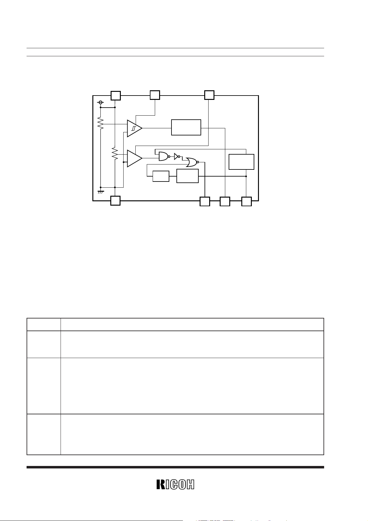
Each of these protectors comprise two voltage detectors, a hysteresis circuit, a reference voltage source, a logic
circuit, a short-circuit protector and a charger connection detection-circuit. Of the two voltage detectors, VD1
detects overcharging (rising edge of waveform) while VD2 detects excessive discharging (falling edge of waveform).
Voltage output switches to a low (“L”) state if either a rising or falling voltage level is detected. When a short pro-
tection circuit is activated while D
OUT output is at “H” level, DOUT output switches to “L” level after internally set
delay time, which, in turn, switches to “H” level when short is cleared. Required current after detection of over-
discharge is suppressed to minimum by stopping the internal circuit.
Using an external capacitor, the output delay time of the voltage detector for excessive discharge/overcharge
can be set.
The series employ CMOS output type.
APPLICATIONS
•
Li-ion single cell protectors for power pack.
•
High precision protectors for cellular phones, camcorders and any other gadgets using Li-ion cell.
RV5VG1×××
2
BLOCK DIAGRAM
–
+
–
+
8
7
5
4
1
2
3
VDD CT1
CT2
VD1
VD2
Level
Shift
V
SS
DOUT
COUT
V-
Delay
Short
Protect
Charger
Detector
8
7
5
4
1
2
3
RV5VG1×××– ××←Part Number
↑ ↑ ↑
a b c
SELECTION GUIDE
In the RV5VG1×××series, the overcharge/excessive discharge detector threshold, respective hysteresis ranges,
short-circuit detector threshold and taping type can be selected at the user's request.
The selection can be made by designating the part number as shown belows.
}
}
Code
b
Designation of release conditions of voltage detector.
C : VD1 (After over-charge detection)
...................
when battery voltage falls below V
DET1–VHYS1 or a
load resistance is applied.
VD2 (After excessive-discharge detection)
......
when a charger is connected.
D : VD1 (After over-charge detection)
...................
when battery voltage falls below V
DET
1–VHYS1.
VD2 (After excessive-discharge detection)
.....
when battery voltage rises above V
DET2+VHYS2 or a
charger is connected.
a
Development serial number for overcharging/excessive discharge detector threshold, hysteresis
ranges, and short-circuit detector threshold.
c
Designation of Taping Type:
EX. 8pin SSOP: E1, E2
(refer Taping Specifications)
“E2” is prescribed as a standard.
Contents
3
PIN CONFIGURATION
•
8pin SSOP (0.65mm pitch)
1
2
3
4
8
7
6
5
PIN DESCRIPTION
Pin No. Symbol Pin Description
1 DOUT Output Pin of over-discharge detection, CMOS output
2 COUT Output Pin of over-charge detection, CMOS output
3 V- Pin for charger negative input
4 VSS Ground Pin
5 CT
2
Pin for external capacitor for setting output delay of VD2
6 NC No connection
7 CT
1
Pin for external capacitor for setting output delay of VD1
8 VDD Power supply Pin

Absolute Maximum ratings are threshold limit values that must not be exceeded even for an instant under any
conditions. Moreover, such values for any two items must not be reached simultaneously. Operation above
these absolute maximum ratings may cause degradation or permanent damage to the device. These are stress
ratings only and do not necessarily imply functional operation below these limits.
RV5VG1×××
4
ABSOLUTE MAXIMUM RATINGS
Symbol Item Ratings Unit
Topt=25˚C, VSS=0V
VDD Supply Voltage –0.3 to +12 V
V-
VCT1,
V
CT2
Input Voltage
CT1, CT2 pin
V-pin VDD–12 to VDD+0.3
VSS–0.3 to VDD+0.3
V
V
VCOUT
VDOUT
Output Voltage
DOUT pin
COUT pin VDD–12 to VDD+0.3
VSS–0.3 to VDD+0.3
V
V
P
D
Power Dissipation 300 mW
Topt Operating Temperature Range –30 to +80 ˚C
Tstg Storage Temperature Range –55 to +125 ˚C
Tsolder Lead Temperature (Soldering) 260˚C, 10s
ABSOLUTE MAXIMUM RATINGS

RV5VG1×××
5
ELECTRICAL CHARACTERISTICS
• RV5VG101C
Topt=25˚C
Symbol Item Conditions MIN. TYP. MAX. Unit.
VDD1
VDD2
VDET1
Operating Input Voltage
Over-charge Detector
Threshold
VDD to VSS
VDD to V-
Voltage rising edge detection
1.2 5 V
1.2 10 V
4.20 4.25 4.30 V
VHYS1
Over-charge Detector
Hysteresis Range
0.15 0.20 0.25 V
VDET2
Over-discharge Detector
Threshold
Voltage falling edge detection 2.437 2.50 2.563 V
t
VDET1
VDET1 Output Delay Time
C1=1000pF, V
DD
=3.6V→4.3V
22 43 86 ms
t
VDET2
VDET2 Output Delay Time
C2=1000pF, V
DD
=3.6V→2.4V
12 24 48 ms
VOL1 COUT
Nch Tr. ON Voltage
IOL
=100µA, V
DD
=4.4V 0.17 0.5 V
VOH1 COUT Pch Tr. ON Voltage IOH=–100µA, VDD=3.9V 3.4 3.73 V
VOL2 DOUT Nch Tr. ON Voltage IOL=100µA, VDD=2.4V 0.17 0.5 V
VOH2
DOUT Pch Tr. ON Voltage IOH=–100µA, VDD=3.9V 3.4 3.73 V
IDD Supply Current VDD=3.9V, V- =0V 2.3 5.0 µA
Istandby Standby Current VDD=2.4V, V-=2.4V 0.2 2.5 µA
t
short
1
t
short
2
Short protection Delay Time
VDD=3.0V, V-=0V→1V
VDD=2.0V, V-=0V→1V
2.4 4.8 9.6
1.4 2.8 5.6
ms
Vchg
Charger Sense Minimum Voltage
VDD=3.3V 0.13 0.2 V
Rshort V- pin pull down resistance V
DD
=3.9V, V-=1.0V 65 130 260 kΩ
Vshort Short protection Voltage VDD=3.9V 0.17 0.2 0.23 V

Symbol
RV5VG1×××
6
• RV5VG101D
Topt=25˚C
Item Conditions MIN. TYP. MAX. Unit.
VDD1
VDD2
VDET1
Operating Input Voltage
Over-charge Detector
Threshold
VDD to VSS
VDD to V-
Voltage rising edge detection
1.2 5 V
1.2 10 V
4.20 4.25 4.30 V
VHYS1
Over-charge Detector
Hysteresis Range
0.15 0.2 0.25 V
VDET2
Over-discharge Detector
Threshold
Voltage falling edge detection 2.437 2.50 2.563 V
t
VDET1
VDET1 Output Delay Time
C1=1000pF, V
DD
=3.6V→4.3V
22 43 86 ms
t
VDET2
VDET2 Output Delay Time
C2=1000pF, V
DD
=3.6V→2.4V
12 24 48 ms
VOL1 COUT Nch Tr. ON Voltage IOL=100µA, VDD=4.4V 0.17 0.5 V
VOH1 COUT Pch Tr. ON Voltage IOH=–100µA, VDD=3.9V 3.4 3.73 V
VOL2 DOUT Nch Tr. ON Voltage IOL=100µA, VDD=2.4V 0.17 0.5 V
VOH2
DOUT Pch Tr. ON Voltage IOH=–100µA, VDD=3.9V 3.4 3.73 V
IDD Supply Current VDD=3.9V, V- =0V 2.3 5.0 µA
Istandby Standby Current VDD=2.4V, V-=2.4V 1.0 2.5 µA
t
short
1
t
short
2
Short protection Delay Time
VDD=3.0V, V-=0V→1V
VDD=2.0V, V-=0V→1V
2.4 4.8 9.6
1.4 2.8 5.6
ms
Vchg
Charger Sense MinimumVoltage
VDD=2.9V 0.1 0.2 V
Rshort V- pin pull down resistance V
DD
=3.9V, V-=1.0V 65 130 260 kΩ
Vshort Short protection Voltage VDD=3.9V 0.17 0.2 0.23 V
VHYS2
Over-discharge Detector
Hysteresis Range
0.50 0.60 0.70 V

RV5VG1×××
7
TYPICAL APPLICATION
RV5VG1×××
0.1µF
0.1µF
0.1µF
100Ω
1KΩ
1000pF 1000pF
+
–
8
7
5
3
2
1
4
V
DD
CT1
CT2
VSS
DOUT
COUT
V-
C1
C2

RV5VG1×××
8
TAPING SPECIFICATION (Unit: mm)
User Direction of Feed.
E1 E2
2.7MAX.
0.3±0.1
4.0±0.1
2.0±0.05
8.0±0.1
1.75±0.1
5.5±0.05
3.7
6.9
12.0±0.3
ø1.5
+0.1
–0
PACKAGE DIMENSIONS (Unit: mm)
• 8pin SSOP (0.65mm pitch)
• 8pin SSOP (0.65mm pitch)
0.575 TYP.
3.1±0.3
6.4±0.3
4.4±0.2
0.22±0.1
0.5±0.3
1.15±0.1
0.1±0.1
0.15
0.15
M
0.15
+0.1
–0.05
0.65

RICOH COMPANY, LTD.
ELECTRONIC DEVICES DIVISION
HEADQUARTERS
13-1, Himemuro-cho, Ikeda City, Osaka 563-8501, JAPAN
Phone 81-727-53-1111 Fax 81-727-53-6011
YOKOHAMA OFFICE (International Sales)
3-2-3, Shin-Yokohama, Kohoku-ku, Yokohama City, Kanagawa 222-8530,
JAPAN
Phone 81-45-477-1697 Fax 81-45-477-1694 · 1695
http://www.ricoh.co.jp/LSI/english/
RICOH CORPORATION
ELECTRONIC DEVICES DIVISION
SAN JOSE OFFICE
3001 Orchard Parkway, San Jose, CA 95134-2088, U.S.A.
Phone 1-408-432-8800 Fax 1-408-432-8375
NOTICE
1. The products and the product specifications described in this document are subject to change or discontinuation
of production without notice for reasons such as improvement. Therefore, before deciding to use the products,
please refer to Ricoh sales representatives for the latest information thereon.
2. This document may not be copied or otherwise reproduced in whole or in part without prior written consent of
Ricoh.
3. Please be sure to take any necessary formalities under relevant laws or regulations before exporting or otherwise taking out of your country the products or the technical information described herein.
4. The technical information described in this document shows typical characteristics of and example application
circuits for the products. The release of such information is not to be construed as a warranty of or a grant of
license under Ricoh's or any third party's intellectual property rights or any other rights.
5. The products listed in this document are intended and designed for use as general electronic components in
standard applications (office equipment, computer equipment, measuring instruments, consumer electronic
products, amusement equipment etc.). Those customers intending to use a product in an application requiring
extreme quality and reliability, for example, in a highly specific application where the failure or misoperation of
the product could result in human injury or death (aircraft, spacevehicle, nuclear reactor control system, traffic
control system, automotive and transportation equipment, combustion equipment, safety devices, life support
system etc.) should first contact us.
6. We are making our continuous effort to improve the quality and reliability of our products, but semiconductor
products are likely to fail with certain probability. In order prevent any injury to persons or damages to property
resulting from such failure, customers should be careful enough to incorporate safety measures in their design,
such as redundancy feature, fire-containment feature and fail-safe feature. We do not assume any liability or
responsibility for any loss or damage arising from misuse or inappropriate use of the products.
7. Anti-radiation design is not implemented in the products described in this document.
8. Please contact Ricoh sales representatives should you have any questions or comments concerning the products or the technical information.
1995 June
 Loading...