

Page 1

1
3-WIRE SERIAL INTERFACE REAL-TIME CLOCK IC
WITH VOLTAGE MONITORING FUNCTION
RV5C339A
OUTLINE
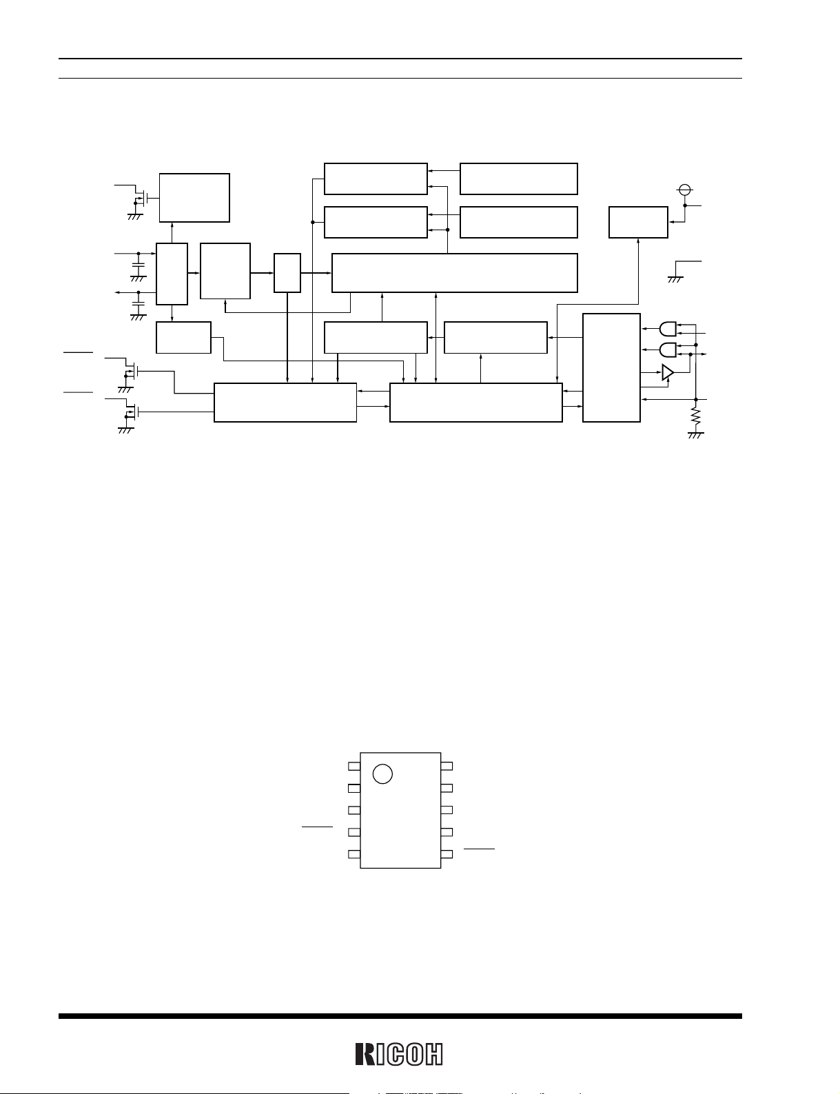
The RV5C339A is a CMOS real-time clock IC connected to the CPU by three signal lines CE (Chip Enable), SCLK
(Serial Clock), and SIO (Serial Input/Output), and configured to perform serial transmission of time and calendar
data to the CPU. This model incorporates different functional circuits. The periodic interrupt circuit is configured
to generate interrupt signals with six selectable interrupts ranging from 0.5 seconds to 1 month. The 2 alarm
circuits generate interrupt signals at preset times. The oscillation circuit is driven under constant voltage so that
fluctuations in oscillation frequency due to voltage are small and supply current is also small (TYP. 0.35µA at 3
volts). The oscillation halt sensing circuit can be used to judge the validity of internal data in such events as poweron. The supply voltage monitoring circuit is configured to record a drop in supply voltage below two selectable
supply voltage monitoring threshold settings. The 32-kHz clock output function (Nch. open drain) is intended to
output sub-clock pulses for the external microcomputer. The oscillation adjustment circuit is intended to adjust time
counts with high precision by correcting deviations in the oscillation frequency of the crystal oscillator. This model
comes in an ultra-compact 10-pin SSOP-G (with a height of 1.20mm and a pin pitch of 0.5mm).
FEATURES
• Timekeeping supply voltage ranging from 1.45 to 5.5 volts
• Low supply current: TYP. 0.35µA (MAX. 0.8µA) at 3 volts (at 25˚C)
• Only three signal lines (SCLK, SIO, and CE) required for connection to the CPU.
Maximum clock frequency of 2 MHz (with V
DD of 5 volts)
• Time counters (counting hours, minutes, and seconds) and calendar counters (counting years, months, days, and
weeks) (in BCD format)
• 1900/2000 identification bit for Year 2000 compliance
• Interrupt circuit configured to generate interrupt signals (with interrupts ranging from 0.5 seconds to 1 month) to
the CPU and provided with an interrupt flag and an interrupt halt circuit
•2 alarm circuits (Alarm_W for week , hour , and minute alarm settings and Alarm_D for hour and minute alarm
settings)
• 32-kHz clock circuit (Nch. open drain output)
Designed to disable 32-kHz clock output in response to a command from the host computer.
• Oscillation halt sensing circuit which can be used to judge the validity of internal data
• Supply voltage monitoring circuit with two supply voltage monitoring threshold settings
• Automatic identification of leap years up to the year 2099
• Selectable 12-hour and 24-hour mode settings
• Built-in oscillation stabilization capacitors (C
G and CD)
• High precision oscillation adjustment circuit
• CMOS process
NO.EA-055-0208
Page 2
RV5C339A
2
BLOCK DIAGRAM
COMPARATOR_W
ALARM_W REGISTER
(MIN,HOUR,WEEK)
ALARM_D REGISTER
(MIN,HOUR)
COMPARATOR_D
TIME COUNTER
(SEC,MIN,HOUR,WEEK,DAY,MONTH,YEAR)
ADDRESS
REGISTER
ADDRESS
DECODER
SHIFT REGISTER
INTERRUPT CONTROL
32kHz
OUTPUT
CONTROL
DIVIDER
CORREC
-TION
DIV
OSC
OSCIN
32KOUT
OSCOUT
OSC
DETECT
I/O
CONTROL
VSS
SCLK
SIO
CE
VDD
INTRB
INTRA
VOLTAGE
DETECT
PIN CONFIGURATION
32KOUT
1
SCLK
2
SIO
3
VSS
INTRB
VDD
OSCIN
OSCOUT
CE
INTRA
4
5
8
9
10
7
6
• 10-pin SSOP-G
APPLICATIONS
• Communication devices (multi function phone, portable phone, PHS or pager)
• OA devices (fax, portable fax)
• Computer (desk-top and mobile PC, portable word-processor, PDA, electric note or video game)
• AV components (portable audio unit, video camera,camera, digital camera or remote controller)
• Home appliances (rice cooker, electric oven)
• Other (car navigation system, multi-function watch)
Page 3

3
RV5C339A
PIN DESCRIPTIONS
Pin No.
Symbol Name Description
7CEChip Enable Input
The CE pin is used for interfacing with the CPU. Should be held high to allow
access to the CPU. Incorporates a pull-down resistor. Should be held low or open
when the CPU is powered off. Allows a maximum input voltage of 5.5 volts regard-
less of supply voltage.
2 SCLK Serial Clock Input
The SCLK pin is used to input clock pulses synchronizing the input and output of
data to and from the SIO pin. Allows a maximum input voltage of 5.5 volts regard-
less of supply voltage.
3 SIO
Serial Input/Output
The SIO pin is used to input and output data intended for writing and reading in
synchronization with the SCLK pin. CMOS input/output.
6INTRA Interrupt Output A
The INTRA pin is used to output periodic interrupt signals to the CPU and alarm
interrupt signals (Alarm_D). Disabled at power-on from 0 volts.
Nch. open drain output.
4 INTRB Interrupt Output B
The INTRB pin is used to output alarm interrupt signals (Alarm_W). Disable at
power-on from 0 volts. Nch. open drain output.
1 32KOUT
32-kHz Clock Output
The 32KOUT pin is used to output 32.768-kHz clock pulses. Enabled at power-on
from 0 volts. Nch. open drain output. The RV5C339A is designed to be disabled
32-kHz clock output in response to a command from the host computer.
The OSCIN and OSCOUT pins are used to connect the 32.768-kHz crystal oscilla-
tor (with all other oscillation circuit components built into the RV5C339A.)
The VDD pin is connected to the power supply. The VSS pin is grounded.
9 OSCIN Oscillation Circuit
8
OSCOUT
Input/Output
10 VDD
Positive Power Supply Input
5 VSS
Negative Power Supply Input
Page 4
RV5C339A
4
RECOMMENDED OPERATING CONDITIONS
(Vss=0V,Topt=–40 to +85˚C)
Symbol Item Conditions MIN. TYP. MAX. Unit
VDD Supply Voltage 2.0 5.5 V
VCLK Timekeeping Voltage 1.45 5.5 V
fXT Oscillation Frequency 32.768 kHz
V
PUP
Pull-up Voltage 32KOUT, INTRA, INTRB 5.5 V
ABSOLUTE MAXIMUM RATINGS
Absolute Maximum ratings are threshold limit values that must not be exceeded even for an instant under
any conditions. Moreover, such values for any two items must not be reached simultaneously. Operation
above these absolute maximum ratings may cause degradation or permanent damage to the device. These
are stress ratings only and do not necessarily imply functional operation below these limits.
ABSOLUTE MAXIMUM RATINGS
Symbol Item Conditions Ratings Unit
VDD Supply Voltage –0.3 to +6.5 V
VI
Input Voltage 1 SIO –0.3 to V
DD+0.3
V
Input Voltage 2 SCLK, CE –0.3 to +6.5
V
O
Output Voltage 1 SIO –0.3 to V
DD+0.3
V
Output Voltage 2 32KOUT, INTRA, INTRB –0.3 to +6.5
P
D Power Dissipation Topt=25˚C 300 mW
Topt Operating Temperature –40 to +85 ˚C
Tstg Storage Temperature –55 to +125 ˚C
(Vss=0V)
Page 5
5
RV5C339A
DC ELECTRICAL CHARACTERISTICS
Symbol Item Pin name Conditions MIN. TYP. MAX. Unit
VIH1
“H” Input Voltage SCLK,CE 0.8VDD 5.5
V
IH2 “H” Input Voltage SIO V
DD=2.0 to 5.5V 0.8V
DD
VDD+0.3
V
V
IL “L” Input Voltage SCLK,CE,SIO –0.3 0.2VDD
IOH “H” Output Current SIO V
OH=V
DD–0.5V –0.5 mA
I
OL1
32KOUT,
V
OL
=0.4V 2
”L” Output Current INTRA, INTRB
mA
IOL2 SIO VOL=0.4V 0.5
I
IL
Input Leakage Current
SCLK
V
I=5.5V or Vss
–1 1 µA
VDD=5.5V
RDNCE Pull-down Resistance CE 40 120 400 kΩ
I
OZ1 SIO
Vo=5.5V or Vss
–1 1
µA
Output Off-state
V
DD=5.5V
I
OZ2
Leakage Current
32KOUT,
V
O=5.5V –1 1
INTRA, INTRB
VDD=3V,CE=OPEN
IDD1 Standby Current VDD Output=OPEN 0.35 0.8 µA
32KOUT=Off mode*
1
VDETH
Supply Voltage Monitoring
VDD Topt=–30 to +70˚C 1.90 2.10 2.30 V
Voltage (“H”)
VDETL
Supply Voltage Monitoring
VDD Topt=–30 to +70˚C 1.45 1.60 1.80 V
Voltage (“L”)
CG
Internal Oscillation Capacitance 1
OSCIN 12
pF
C
D
Internal Oscillation Capacitance 2
OSCOUT 12
Unless otherwise specified : Vss=0V,VDD=3V,Topt=–40 to +85˚C
*
1) For standby current for outputting 32.768-kHz clock pulses from the 32KOUT pin, see “USAGES, 7. Typical Characteristics”.
Page 6
RV5C339A
6
Symbol Item Conditions
V
DD≥2.0V VDD≥4.5V
Unit
MIN. TYP. MAX. MIN. TYP. MAX.
tCES CE Set-up Time 400 200 ns
tCEH CE Hold Time 400 200 ns
tCR
CE Recovery Time 62 62 µs
fSCLK SCLK Clock Frequency 1.0 2.0 MHz
tCKH SCLK Clock “H” Time 400 200 ns
tCKL SCLK Clock “L” Time 400 200 ns
t
CKS SCLK Set-up Time 200 100 ns
tRD Data Output Delay Time 300 150 ns
tRZ Data Output Floating Time 300 150 ns
tCEZ
Data Output Floating Time
300 150 ns
After Falling of CE
tDS Input Data Set-up Time 200 100 ns
tDH Input Data Hold Time 200 100 ns
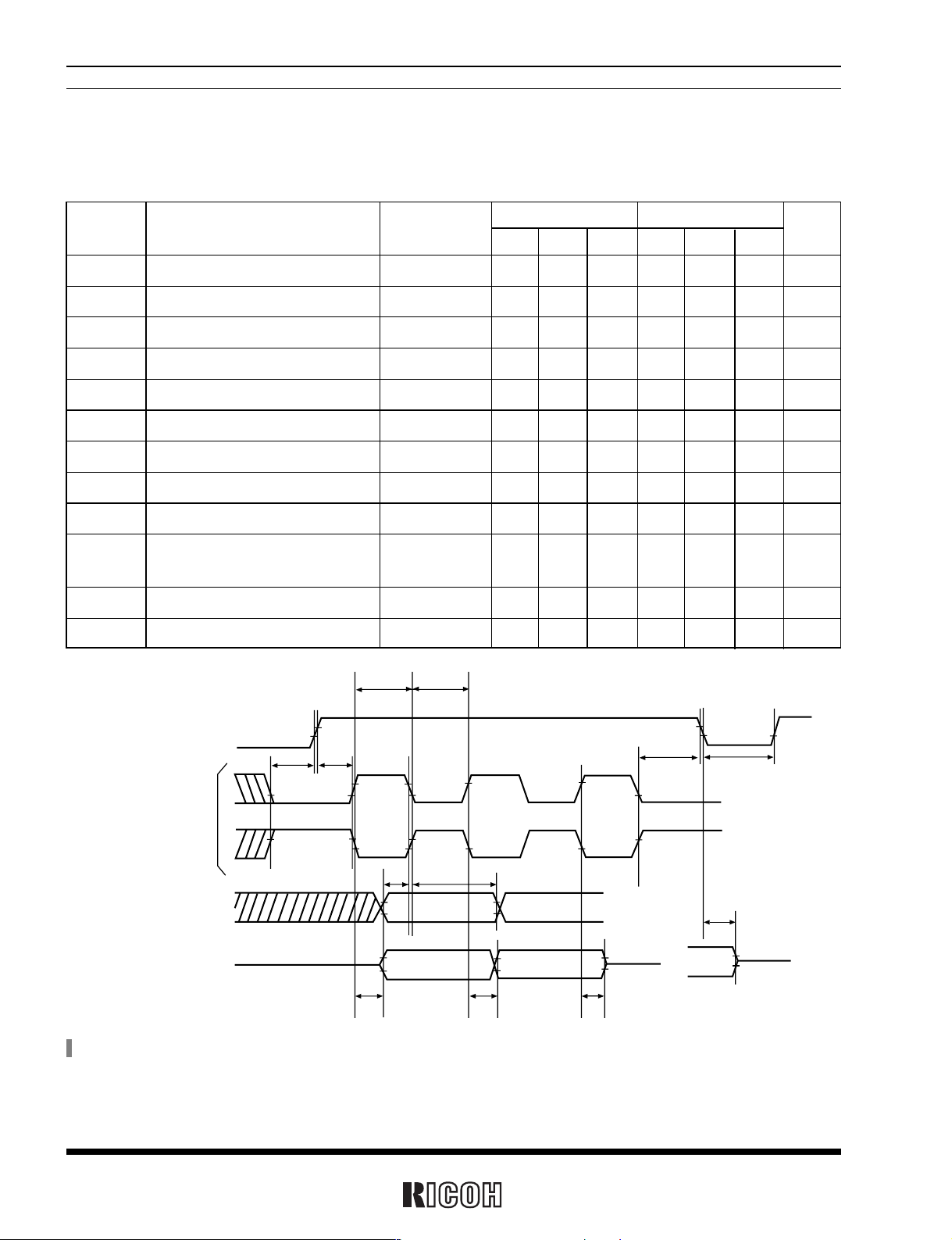
AC ELECTRICAL CHARACTERISTICS
Unless otherwisespecified : Vss=0V, Topt=–40 to +85˚C, CL=50pF
Input/output conditions : V
IH=0.8 × VDD, VIL=0.2 × VDD, VOH=0.8 × VDD, VOL=0.2 × VDD
CE
SCLK
SIO (Write cycle)
SIO (Read cycle)
tCKH tCKL
tCKS
tCES
tDS tDH
tRD
tRD
tRZ
tCEZ
tCEH
tCR
*
) For read/write timing, see Paragraph “USAGES, 1.5 Considerations in Reading and Writing Time Data”
Page 7

7
RV5C339A
GENERAL DESCRIPTION
1. Interface with CPU
The RV5C339A is connected to the CPU by three signal lines CE (Chip Enable), SCLK (Serial Clock), SIO (Serial
Input/Output), through which it reads and write data from and to the CPU. The CPU can access when the CE pin is
held high. Access clock pulses have a maximum frequency of 2MHz (at 5 volts), allowing high-speed data transfer
to the CPU.
2. Clock and Calendar Function
The RV5C339A reads and writes time data from and to the CPU in units ranging from seconds to the last two digits
of the calendar year. The calendar year will automatically be identified as a leap year when its last two digits are a
multiple of 4. Also available is the 1900/2000 identification bit for Year 2000 compliance. Consequently, leap years
up to the year 2099 can automatically be identified as such.
*
) The year 2000 is a leap year while the year 2100 is not a leap year.
3. Alarm Function
The RV5C339A incorporates an alarm circuit configured to generate interrupt signals to the CPU for output at preset
times. The alarm circuit allows two types of alarm settings specified by the Alarm_W registers and the Alarm_D
registers. The Alarm_W registers allow week, hour, and minute alarm settings including combinations of multiple
day-of-week settings such as “Monday, Wednesday, and Friday” and “Saturday and Sunday”. The Alarm_D regis-
ters allow hour and minute alarm settings. The Alarm_D signal outputs from INTRA pin, and the Alarm_W signal
outputs from INTRB pin. The current INTRA or INTRB conditions specified by the flag bits for each alarm function
can be checked from the CPU by using polling function.
4. High-precision Oscillation Adjustment Function
The RV5C339A has built-in oscillation stabilization capacitors (CG and CD), which can be connected to an external
crystal oscillator to configure an oscillation circuit. To correct deviations in the oscillation frequency of the crystal
oscillator, the oscillation adjustment circuit is configured to allow correction of a time count gain or loss (up to ±1.5
ppm at 25˚C) from the CPU within a maximum range of approximately ±189 ppm in increments of approximately 3
ppm. Such oscillation frequency adjustment in each system has the following advantages:
· Allows timekeeping with much higher precision than conventional real-time clocks while using a crystal oscillator
with a wide range of precision variations.
· Corrects seasonal frequency deviations through seasonal oscillation adjustment.
· Allows timekeeping with higher precision particularly in systems with a temperature sensing function through
oscillation adjustment in tune with temperature fluctuations.
Page 8

RV5C339A
8
5. Oscillation Halt Sensing Function and Supply Voltage Monitoring Function
The RV5C339A incorporates an oscillation halt sensing circuit equipped with internal registers configured to record
any past oscillation halt, thereby identifying whether they are powered on from 0 volts or battery backed-up. As
such, the oscillation halt sensing circuit is useful for judging the validity of time data.
The RV5C339A also incorporates a supply voltage monitoring circuit equipped with internal registers configured to
record any drop in supply voltage below a certain threshold value. Supply voltage monitoring threshold settings can
be selected between 2.1 and 1.6 volts through internal register settings.
The oscillation halt sensing circuit is configured to confirm the established invalidation of time data in contrast to
the supply voltage monitoring circuit intended to confirm the potential invalidation of time data. Further, the supply
voltage monitoring circuit can be applied to battery supply voltage monitoring.
6. Periodic Interrupt Function
The RV5C339A incorporates a periodic interrupt circuit configured to generate periodic interrupt signals aside from
interrupt signals generated by the alarm circuit for output from the INTRA pin. Periodic interrupt signals have five
selectable frequency settings of 2Hz (once per 0.5 seconds), 1Hz (once per 1 second), 1/60Hz (once per 1 minute),
1/3600Hz (once per 1 hour), and monthly (the first day of every month). Further, periodic interrupt signals also
have two selectable waveforms of a normal pulse form (with a frequency of 2Hz or 1Hz) and special form adapted to
interruption from the CPU in the level mode (with second, minute, hour, and month interrupts). The condition of
periodic interrupt signals can be monitored by using a polling function.
7. 32-kHz Clock Output Function
The RV5C339A incorporates a 32-kHz clock circuit configured to generate clock pulses with the oscillation frequen-
cy of a 32.768-kHz crystal oscillator for output from the 32KOUT pin. The 32KOUT pin is Nch. open drain output.
The 32-kHz clock output can be disabled by certain register settings But it cannot be disabled without manipulation
of any two registers with different addresses, to prevent disabling in such events as the runaway of the CPU.
Page 9
9
RV5C339A
Data*
1
00 000Second Counter –
*
2
S40 S20
S10 S
8 S4 S2 S1
10 001Minute Counter – M
40 M
20 M10 M8
M4 M2 M1
20 0 1 0
Hour Counter
––
H
20
H10 H
8 H4 H2 H1
P/A
30 011Day-of-week Counter – – – – – W4 W2 W1
40 100Day-of-month Counter – – D
20 D10 D8 D4 D2 D1
50 1 0 1
Month counter and Century Bit
19/20 – – MO10 MO8 MO4 MO2 MO1
60 110Year Counter Y
80 Y40 Y20 Y10 Y8 Y4 Y2 Y1
70 1 1 1
Oscillation Adjustment Register
*
3
(0)*4F6 F5 F4 F3 F2 F1 F0
81 0 0 0
Alarm_W (minute register)
–WM40 WM20 WM10 WM8 WM4 WM2 WM1
91 001Alarm_W (hour register) – –
WH
20
WH
10 WH8 WH4 WH2 WH1
WP/A
A1 0 1 0
Alarm_W
(day-of-week register)
–WW
6 WW5 WW4 WW3 WW2 WW1 WW0
B1 011Alarm_D (minute register) – DM40 DM20 DM10 DM8 DM4 DM2 DM1
C1 100Alarm_D (hour register) – –
DH20
DH10 DH8 DH4 DH2 DH1
DP/A
D1 101––––––––
E1 110Control Register 1*
3
WALE DALE 12/24
CLEN2
TEST CT2 CT1 CT0
F1 111Control Register 2*
3
VDSL VDET
SCRATCH
XSTP
CLEN1
CTFG WAFG DAFG
D3 D2
D1
D0
Address
A3
A2 A1 A0
Register
D4D5D6D7
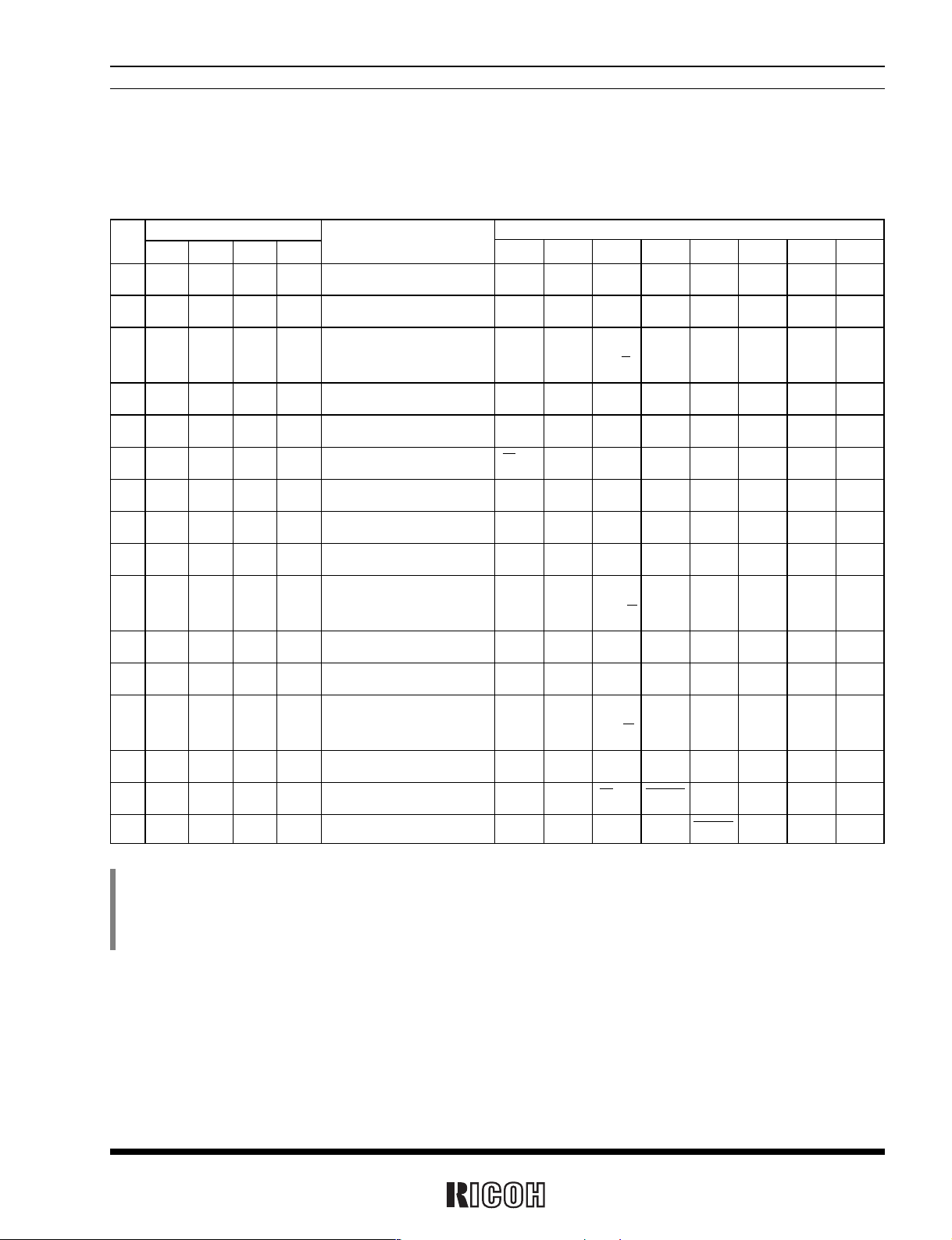
FUNCTIONAL DESCRIPTIONS
1. Address Mapping
*
1) All the data listed above accept both reading and writing.
*
2) The data marked with “–” is invalid for writing and reset to 0 for reading.
*
3) When the XSTP bit is set to 1 in control register 2, all the bits are reset to 0 in oscillation adjustment register 1, control register 1 and control register 2
excluding the XSTP bit.
*
4) Writing to the oscillation adjustment register requires zero filling the (0) bit.
Page 10
RV5C339A
10
WALE, DALE Description
0
Disabling the alarm interrupt circuit (under the control of the settings of the
Alarm_W registers and the Alarm_D registers).
1
Enabling the alarm interrupt circuit (under the control of the settings of the
Alarm_W registers and the Alarm_D registers)
D7 D6 D5 D4 D3 D2 D1 D0
WALE DALE 12/24 CLEN2 TEST CT
2 CT1 CT
0
WALE DALE 12/24 CLEN2 TEST CT
2 CT
1 CT0
00000000
(For writing)
(For reading)
Default settings*
(Default setting)
2. Register Settings
2.1 Control Register 1 (at Address Eh)
*
) Default settings: Default value means read/written values when the XSTP bit is set to “1” due to power-on from 0 volts or supply voltage drop.
2.1-1 WALE, DALE
Alarm_W Enable Bit and Alarm_D Enable Bit
2.1-2 12/24-hour Mode Selection Bit
12/24-hour Time Display System Selection bit
12/24 Description
0 Selecting the 12-hour mode with a.m. and p.m. indications.
1 Selecting the 24-hour mode
Setting the 12/24 bit to 0 and 1 specifies the 12-hour mode and the 24-hour mode, respectively.
Table of Time Digit Indications
24-hour mode 12-hour mode 24-hour mode 12-hour mode
00 12 (AM12) 12 32 (PM12)
01 01 (AM 1) 13 21 (PM 1)
02 02 (AM 2) 14 22 (PM 2)
03 03 (AM 3) 15 23 (PM 3)
04 04 (AM 4) 16 24 (PM 4)
05 05 (AM 5) 17 25 (PM 5)
06 06 (AM 6) 18 26 (PM 6)
07 07 (AM 7) 19 27 (PM 7)
08 08 (AM 8) 20 28 (PM 8)
09 09 (AM 9) 21 29 (PM 9)
10 10 (AM10) 22 30 (PM10)
11 11 (AM11) 23 31 (PM11)
*
) Setting the 12/24 bit should precede writing time data.
Page 11

11
RV5C339A
2.1-5 CT2
, CT1, and CT
0
1) Pulse Mode : 2-Hz and 1-Hz clock pulses are output in synchronization with the increment of the second counter
as illustrated in the timing chart on the next page.
TEST Description
0 Normal operation mode
1 Test mode
2.1-4 TEST
Test Bit
(Default setting)
The TEST bit is used only for testing in the factory and should normally be set to 0.
Periodic Interrupt Selection Bits
CT
2 CT1 CT
0
Description
Waveform mode
Interrupt cycle and falling timing
000 — Off (“H”)
001 — Fixed at low (“L”)
010Pulse Mode 2Hz (Duty cycle of 50%)
011Pulse Mode 1Hz (Duty cycle of 50%)
100Level Mode Once per 1 second (Synchronized with second counter increment)
101Level Mode Once per minute (at 00 seconds of every minute)
110Level Mode Once per hour (at 00 minutes and 00 seconds of every hour)
111Level Mode
Once per month (at 00 hours, 00 minutes, and 00 seconds of first day of every month)
(Default setting)
2.1-3 CLEN2
32-kHz Clock Output Bit 2
CLEN2 Description
0 Enabling the 32-kHz clock circuit
1 Disabling the 32-kHz clock circuit
(Default setting)
Setting the CLEN2 bit or the CLEN1 bit (D3 in the control register 2) to 0, specifies generating clock pulses with
the oscillation frequency of the 32.768-kHz crystal oscillator for output from the 32KOUT pin. Conversely, setting
both the CLEN1 and the CLEN2 bit to 1 disabling (“H”) such output.
Page 12
RV5C339A
12
Relation Between the Mode Waveform and the CTFG Bit
• Pulse mode
Approx. 92µs
CTFG bit
INTRA pin
(Increment of second counter)
Rewriting of the second counter
• Level mode
Setting CTFG bit to 0
(Increment of
second counter)
Setting CTFG bit to 0
CTFG bit
INTRA pin
(Increment of
second counter)
(Increment of
second counter)
*
) In the pulse mode, the increment of the second counter is delayed by approximately 92µs from the falling edge of clock pulses. Consequently, time
readings immediately after the falling edge of clock pulses may appear to lag behind the time counts of the real-time clocks by approximately 1 second.
Rewriting the second counter will reset the other time counters of less than 1 second, driving the INTRA pin low.
2) Level Mode : periodic interrupt signals are output with selectable interrupt cycle settings of 1 second, 1 minute, 1
hour, and 1 month. The increment of the second counter is synchronized with the falling edge of
periodic interrupt signals. For example, periodic interrupt signals with an interrupt cycle setting of
1 second are output in synchronization with the increment of the second counter as illustrated in
the timing chart below.
3) When the oscillation adjustment circuit is used, the interrupt cycle will fluctuate once per 20 seconds as follows:
Pulse Mode : the “L” period of output pulses will increment or decrement by a maximum of ±3.784ms.
For example, 1-Hz clock pulses will have a duty cycle of 50 ±0.3784%.
Level Mode : a periodic interrupt cycle of 1 second will increment or decrement by a maximum of ±3.784ms.
Page 13
13
RV5C339A
VDSL Description
0 Selecting the supply voltage monitoring threshold setting of 2.1 volts.
1 Selecting the supply voltage monitoring threshold setting of 1.6 volts.
2.2-1 VDSL
Supply Voltage Monitoring Threshold Selection Bit
The VDSL bit is intended to select the supply voltage monitoring threshold settings.
VDET Description
0
Indicating supply voltage above the supply voltage monitoring threshold settings.
1
Indicating supply voltage below the supply voltage monitoring threshold settings.
2.2-2 VDET
Supply Voltage Monitoring Result Indication Bit
(Default setting)
Once the VDET bit is set to 1, the supply voltage monitoring circuit will be disabled while the VDET bit will hold the
setting of 1. The VDET bit accepts only the writing of 0, which restarts the supply voltage monitoring circuit.
Conversely, setting the VDET bit to 1 causes no event.
D7 D6 D5 D4 D3 D2 D1 D0
VDSL VDET
SCRATCH
XSTP CLEN1 CTFG WAFG DAFG
VDSL VDET
SCRATCH
XSTP CLEN1 CTFG WAFG DAFG
00010000
2.2 Control Register 2 (at Address Fh)
(For writing)
(For reading)
Default setting*
SCRATCH Description
0
1
2.2-3 SCRATCH
Scratch Bit
(Default setting)
The SCRATCH bit is intended for scratching and accepts the reading and writing of 0 and 1. The SCRATCH bit will
be set to 0 when the XSTP bit is set to 1 in the control register 2.
(Default setting)
*
) Default settings: Default value means read/written values when the XSTP bit is set to “1” due to power-on from 0 volts or supply voltage drop.
Page 14
RV5C339A
14
2.2-4 XSTP
Oscillator Halt Sensing Bit
CLEN1 Description
0 Enabling the 32-kHz clock output
1 Disabling the 32-kHz clock output
2.2-5 CLEN1
32-kHz Clock Output Bit 1
(Default setting)
CTFG Description
0 Periodic interrupt output “H” (OFF)
1 Periodic interrupt output “L” (ON)
2.2-6 CTFG
Periodic Interrupt Flag Bit
(Default setting)
The CTFG bit is set to 1 when the periodic interrupt signals are output from the INTRA pin (“L”). The CTFG bit
accepts only the writing of 0 in the level mode, which disables (“H”) the INTRA pin until it is enabled (“L”) again in
the next interrupt cycle. Conversely, setting the CTFG bit to 1 causes no event.
Setting the CLEN1 bit or the CLEN2 bit (D4 in control register 1) to 0 specifies generating clock pulses with the
oscillation frequency of the 32.768-kHz crystal oscillator for output from the 32KOUT pin. Conversely, setting both
the CLEN1 bit and the CLEN2 bit to 1 specifies disabling (“H”) such output.
The XSTP bit is for sensing a halt in the oscillation of the crystal oscillator. The oscillation halt sensing circuit
operates only when the CE pin is “L”.
· The XSTP bit will be set to 1 once a halt in the oscillation of the crystal oscillator is caused by such events as pow-
er-on from 0 volts and a drop in supply voltage. The XSTP bit will hold the setting of 1 even after the restart of
oscillation. As such, the XSTP bit can be applied to judge the validity of clock and calendar data after power-on or
a drop in supply voltage.
· When the XSTP bit is set to 1, all bits will be reset to 0 in the oscillation adjustment register, control register 1, and
control register 2, stopping the output from the INTRA and INTRB pin and starting the output of 32.768-kHz clock
pulses from the 32KOUT pin.
· The XSTP bit accepts only the writing of 0, which restarts the oscillation halt sensing circuit. Conversely, setting
the XSTP bit to 1 causes no event.
XSTP Description
0 Sensing a normal condition of oscillation
1 Sensing a halt of oscillation
(Default setting)
Page 15

15
RV5C339A
WAFG, DAFG Description
0 Indicating a mismatch between current time and preset alarm time
1 Indicating a match between current time and preset alarm time
2.2-7 WAFG and DAFG
Alarm_W Flag Bit and Alarm_D Flag Bit
(Default setting)
The WAFG and DAFG bits are valid only when the WALE and DALE bits have the setting of 1, which is caused
approximately 61µs after any match between current time and preset alarm time specified by the Alarm_W registers
and the Alarm_D registers. The WAFG and DAFG bits accept only the writing of 0, which disables (“H”) the
INTRA(or INTRB) pin until it is enabled (“L”) again at the next preset alarm time. Conversely, setting the WAFG
and DAFG bits to 1 causes no event. The WAFG and DAFG bits will have the reading of 0 when the alarm interrupt
circuit is disabled with the WALE and DALE bits set to 0.
Output Relationships Between the WAFG or DAFG Bit and INTRA, INTRB
Writing of 0 to WAFG
(DAFG) bit
(Match between current time
and preset alarm time)
(Match between current time
and preset alarm time)
(Match between current time
and preset alarm time)
Writing of 0 to WAFG
(DAFG) bit
Settings of WAFG (DAFG) bit
Output of INTRA (INTRB) pin
Approx. 61µs Approx. 61µs
Page 16
RV5C339A
16
2.3 Time Counters (at Addresses 0h to 2h)
· Time digit display (BCD format) as follows:
The second digits range from 00 to 59 and are carried to the minute digit in transition from 59 to 00.
The minute digits range from 00 to 59 and are carried to the hour digits in transition from 59 to 00.
The hour digits range as shown in “2.1-2 12/24: 12-/24-hour Mode Selection Bit” and are carried to the day-of-
month and day-of-week digits in transition from PM11 to AM12 or from 23 to 00.
· Any writing to the second counter resets divider units of less than 1 second.
· Any carry from lower digits with the writing of non-existent time may cause the time counters to malfunction.
Therefore, such incorrect writing should be replaced with the writing of existent time data.
2.3-1 Second Counter (at Address 0h)
D7 D6 D5 D4 D3 D2 D1 D0
—S40 S20 S10 S8 S4 S2 S1
0S40 S20 S10 S8 S4 S2 S1
0 Indefinite Indefinite Indefinite Indefinite Indefinite Indefinite Indefinite
(For writing)
(For reading)
Default settings*
2.3-2 Minute Counter (at Address 1h)
D7 D6 D5 D4 D3 D2 D1 D0
—M
40 M20 M10 M8 M4 M2 M1
0M40 M20 M10 M8 M4 M2 M1
0 Indefinite Indefinite Indefinite Indefinite Indefinite Indefinite Indefinite
(For writing)
(For reading)
Default settings*
2.3-3 Hour Counter (at Address 2h)
D7 D6 D5 D4 D3 D2 D1 D0
——P/A or H20 H10 H8 H4 H2 H1
00P/A or H20 H10 H8 H4 H2 H1
00Indefinite Indefinite Indefinite Indefinite Indefinite Indefinite
(For writing)
(For reading)
Default settings*
*
) Default settings: Default value means read/written values when the XSTP bit is set to “1” due to power-on from 0 volts or supply voltage drop.
Page 17

17
RV5C339A
2.4 Day-of-week Counter (at Address 3h)
D7 D6 D5 D4 D3 D2 D1 D0
—————W4 W2 W1
00000W
4
W2 W1
00000Indefinite Indefinite Indefinite
(For writing)
(For reading)
Default settings*
*
) Default settings: Default value means read/written values when the XSTP bit is set to “1” due to power-on from 0 volts or supply voltage drop.
· The day-of-week counter is incremented by 1 when the day-of-week digits are carried to the day-of-month digits.
· Day-of-week display (incremented in septimal notation):
(W
4, W2, W1) = (0, 0, 0) → (0, 0, 1) →
...
→ (1, 1, 0) → (0, 0, 0)
· Correspondences between days of the week and the day-of-week digits are user-definable (e.g. Sunday = 0, 0, 0)
· The writing of (1, 1, 1) to (W
4, W2, W1) is prohibited except when days of the week are unused.
2.5 Calendar Counters (at Address 4h to 6h)
· The calendar counters are configured to display the calendar digits in BCD format by using the automatic calen-
dar function as follows:
The day-of-month digits (D
20 to D1) range from 1 to 31 for January, March, May, July, August, October, and
December; from 1 to 30 for April, June, September, and November; from 1 to 29 for February in leap years;
from 1 to 28 for February in ordinary years.
The day-of-month digits are carried to the month digits in reversion from the last day of the month to 1. The
month digits (MO
10 to MO1) range from 1 to 12 and are carried to the year digits in reversion from 12 to 1.
The year digits (Y
80 to Y1) range from 00 to 99 (00, 04, 08, ... , 92, and 96 in leap years) and are carried to the
19/20 digits in reversion from 99 to 00.
The 19/20 digits cycle between 0 and 1 in reversion from 99 to 00 in the year digits.
· Any carry from lower digits with the writing of non-existent calendar data may cause the calendar counters to mal-
function. Therefore, such incorrect writing should be replaced with the writing of existent calendar data.
2.5-1 Day-of-month Counter (at Address 4h)
D7 D6 D5 D4 D3 D2 D1 D0
——D20 D10 D8 D4 D2 D1
00D20 D10 D8 D4 D2 D1
00Indefinite Indefinite Indefinite Indefinite Indefinite Indefinite
(For writing)
(For reading)
Default settings*
2.5-2 Month Counter + Century Bit (at Address 5h)
D7 D6 D5 D4 D3 D2 D1 D0
19/20 — — MO10 MO8 MO4 MO2 MO1
19/20 0 0 MO10 MO8 MO4 MO2 MO1
Indefinite 0 0 Indefinite Indefinite Indefinite Indefinite Indefinite
(For writing)
(For reading)
Default settings*
Page 18

18
RV5C339A
2.5-3 Year Counter (at Address 6h)
D7 D6 D5 D4 D3 D2 D1 D0
Y80 Y40 Y20 Y10 Y8 Y4 Y2 Y1
Y80 Y40
Y20 Y
10 Y8 Y4 Y2 Y
1
Indefinite Indefinite Indefinite Indefinite Indefinite Indefinite Indefinite Indefinite
(For writing)
(For reading)
Default settings*
2.6 Oscillation Adjustment Register (at Address 7h)
D7 D6 D5 D4 D3 D2 D1 D0
(0)
F
6 F5 F4 F3 F2 F1 F0
(0)
F
6 F5 F
4 F3 F2 F1 F0
00000000
(For writing)
(For reading)
Default settings*
*
) Default settings: Default value means read/written values when the XSTP bit is set to “1” due to power-on from 0 volts or supply voltage drop.
2.6-1 (0) Bit
The (0) bit should be set to 0 to allow writing to the oscillation adjustment register. The (0) bit will be set to 0 when
the XSTP bit is set to 1 in the control register 2.
2.6-2 F6 to F0
The oscillation adjustment circuit is configured to change time counts of 1 second on the basis of the settings of the
oscillation adjustment register when the second digits read 00, 20, or 40 seconds. Normally, the second counter is
incremented once per 32768 32.768-kHz clock pulses generated by the crystal oscillator. Writing to the F
6 to F0 bits
activates the oscillation adjustment circuit.
· The oscillation adjustment circuit will not operate with the same timing (00, 20, or 40 seconds) as the timing of
writing to the oscillation adjustment register.
· The F
6 bit setting of 0 causes an increment of time counts by ((F5, F4, F3, F2, F1, F0) –1) × 2.
The F
6 bit setting of 1 causes a decrement of time counts by (( F5, F4, F3, F2, F1, F0) +1) × 2.
The settings of “
*
, 0, 0, 0, 0, 0, *” ( “*” representing either “0” or “1” ) in the F6, F5, F4, F3, F2, F1, and F0 bits
cause neither an increment nor decrement of time counts.
Example:
When the second digits read 00, 20, or 40, the settings of “0, 0, 0, 0, 1, 1, 1” in the F
6, F5, F4, F3, F2, F1, and F0 bits
cause an increment of the current time counts of 32768 by (7–1) × 2 to 32780 (a current time count loss). When the
second digits read 00, 20, or 40, the settings of “0, 0, 0, 0, 0, 0, 1” in the F
6, F5, F4, F3, F2, F1, and F0 bits cause neither
an increment nor a decrement of the current time counts of 32768.
When the second digits read 00, 20, or 40, the settings of “1, 1, 1, 1, 1, 1, 0” in the F
6, F5, F4, F3, F2, F1, and F0 bits
cause a decrement of the current time counts of 32768 by (–2) × 2 to 32764 (a current time count gain).
*
) Default settings: Default value means read/written values when the XSTP bit is set to “1” due to power-on from 0 volts or supply voltage drop.
Page 19

19
RV5C339A
2.7 Alarm_W Register (at Address 8h to Ah)
D7 D6 D5 D4 D3 D2 D1 D0
—WM40 WM20 WM10 WM8 WM4 WM2 WM1
0WM
40 WM20
WM10 WM8 WM4 WM2 WM1
0
Indefinite Indefinite Indefinite Indefinite Indefinite Indefinite Indefinite
(For writing)
(For reading)
Default settings*
2.7-1 Alarm_W Minute Register (at Address 8h)
D7 D6 D5 D4 D3 D2 D1 D0
——
WH20,WP/A
WH10 WH8 WH4 WH2 WH1
00
WH20,WP/A
WH10 WH8 WH4 WH2 WH1
00
Indefinite Indefinite Indefinite Indefinite Indefinite Indefinite
(For writing)
(For reading)
Default settings*
2.7-2 Alarm_W Hour Register (at Address 9h)
D7 D6 D5 D4 D3 D2 D1 D0
—WW6 WW5 WW4 WW3 WW2 WW1 WW0
0WW6 WW5 WW4 WW3 WW2 WW1 WW0
0
Indefinite Indefinite Indefinite Indefinite Indefinite Indefinite Indefinite
(For writing)
(For reading)
Default settings*
2.7-3 Alarm_W Day-of-week Register (at Address Ah)
· The D5 bit of the Alarm_W hour register represents WP/A when the 12-hour mode is selected (0 for a.m. and 1
for p.m.). and WH
20 when the 24-hour mode is selected (tens in the hour digits).
· The Alarm _W registers should not have any non-existent alarm time settings. (Note that any mismatch between
current time and preset alarm time specified by the Alarm_W registers may disable the alarm circuit.)
· When the 12-hour mode is selected, the hour digits read 12 and 32 for 0 a.m. and 0 p.m., respectively (see “2.1-2
12/24: 12-/24-hour Mode Selection Bit”).
· WW
0 to WW6 correspond to W4, W2, and W1 of the day-of-week counter with settings ranging from (0, 0, 0) to (1,
1, 0).
· WW
0 to WW6 with respective settings of 0 disable the outputs of the Alarm_W registers.
*
) Default settings: Default value means read/written values when the XSTP bit is set to “1” due to power-on from 0 volts or supply voltage drop.
An increase of two clock pulses once per 20 seconds causes a time count loss of approximately 3ppm (2 / (32768 ×
20=3.051ppm). Conversely, a decrease of two clock pulses once per 20 seconds causes a time count gain of 3ppm.
Consequently, deviations in time counts can be corrected with a precision of ±1.5ppm. Note that the oscillation
adjustment circuit is configured to correct deviations in time counts and not the oscillation frequency of the 32.768-
kHz clock pulses. For further details, see “USAGE, 2.4 Oscillation Adjustment Circuit”.
Page 20

RV5C339A
20
Day-of-week 12-hour mode 24-hour mode
Preset alarm time
Sun. Mon. Tue. Wed. Thu. Fri. Sat.
10-hour
1-hour 10-min
1-min
10-hour
1-hour 10-min
1-min
WW0 WW1
WW2 WW3 WW
4 WW5 WW6
00:00 a.m. on all days 111111112000000
01:30 a.m. on all days 111111101300130
11:59 a.m. on all days 111111111591159
00:00 p.m. on
011111032001200
Mondays to Fridays
01:30 p.m. on Sundays 100000021301330
11:59 p.m. on Mondays,
010101031592359
Wednesdays, and Fridays
Note that the correspondence between WW
0 to WW6
and the days of the week shown in the above table is only an
example and not mandatory.
D7 D6 D5 D4 D3 D2 D1 D0
—DM40 DM20 DM10 DM8 DM4 DM2 DM1
0DM40 DM20 DM10 DM8 DM4 DM2 DM1
0
Indefinite Indefinite Indefinite Indefinite Indefinite Indefinite Indefinite
(For writing)
(For reading)
Default settings*
2.8-1 Alarm_D Minute Register (at Address Bh)
D7 D6 D5 D4 D3 D2 D1 D0
——
DH20,DP/A
DH10 DH8 DH4 DH2 DH1
00
DH20,DP/A
DH10 DH8 DH4 DH2 DH1
00
Indefinite Indefinite Indefinite Indefinite Indefinite Indefinite
(For writing)
(For reading)
Default settings*
2.8-2 Alarm_D Hour Register (at Address Ch)
2.8 Alarm_D Register (at Address Bh and Ch)
*
) Default settings: Default value means read/written values when the XSTP bit is set to “1” due to power-on from 0 volts or supply voltage drop.
· The D5 bit represents DP/A when the 12-hour mode is selected (0 for a.m. and 1 for p.m.). and DH20 when the 24-
hour mode is selected (tens in the hour digits).
· The Alarm_D registers should not have any non-existent alarm time settings. (Note that any mismatch between
current time and preset alarm time specified by the Alarm_D registers may disable the alarm circuit.)
· When the 12-hour mode is selected, the hour digits read 12 and 32 for 0 a.m. and 0 p.m., respectively (see “2.1-2
12/24: 12-/24-hour Mode Selection Bit”).
Example of Alarm Time Setting
Page 21

21
RV5C339A
USAGES
1. Data Transfer Formats
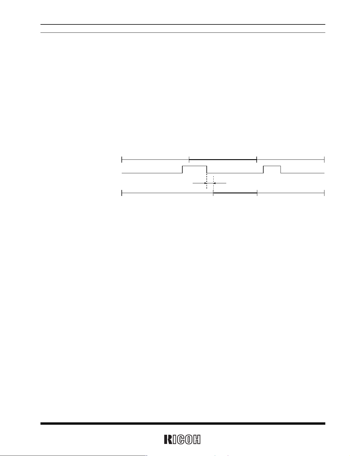
1.1 Timing Between CE Pin Transition and Data Input/Output
The RV5C339A adopts a 3-wire serial interface by which it uses the CE (Chip Enable), SCLK (Serial Clock), and SIO
(Serial Input/Output), pins to receive and send data to and from the CPU. The 3-wire serial interface provides two
types of input/output timings with which the output and input from the SIO pin output and input are synchronized
with the rising and falling edges of the SCLK pin input, respectively, and vice versa. The RV5C339A is configured to
select either one of two different input/output timings depending on the level of the SCLK pin in the low to high
transition of the CE pin. Namely, when the SCLK pin is held low in the low to high transition of the CE pin, the
models will select the timing with which the output and input from the SIO pin are synchronized with the rising and
falling edges of the SCLK pin input, respectively, as illustrated in the timing chart below.
tCES
tDS
tDH
tRD
CE
SCLK
SIO
(Input to the real-time clock)
SIO
(Output from the real-time clock)
Conversely, when the SCLK pin is held high in the low to high transition of the CE pin, the models will select the
timing with which the output and input from the SIO pin are synchronized with the falling and rising edges of the
SCLK pin input, respectively as illustrated in the timing chart below.
tCES
tDS
tDH
tRD
CE
SCLK
SIO
(Input to the real-time clock)
SIO
(Output from the real-time clock)
Page 22

RV5C339A
22
12345678123
A3 A2 A1 A0 C3 C2 C1 C0 D7 D6 D3 D2 D1 D0
CE
SCLK
SIO
Setting the address
pointer
Setting the transfer
format register
Writing data transfer /
Reading data transfer
1.2 Data Transfer Formats
Data transfer is commenced in the low to high transition of the CE pin input and completed in its high to low
transition. Data transfer is conducted serially in multiple units of 1 byte (8 bits). The former 4 bits are used to
specify in the address pointer a head address with which data transfer is to be commenced from the host. The latter
4 bits are used to select either reading data transfer or writing data transfer and set the transfer format register to
specify an appropriate data transfer format. All data transfer formats are designed to transfer the most significant bit
(MSB) first.
Two types of data transfer formats are available for reading data transfer and writing data transfer each.
1.3 Writing Data Transfer Formats
1.3-1 1-byte Writing Data Transfer Format
The first type of writing data transfer format is designed to transfer 1-byte data at a time and can be selected by
specifying in the address pointer a head address with which writing data transfer is to be commenced and then
writing the setting of 8h to the transfer format register. This 1-byte writing data transfer can be completed by
driving the CE pin low or continued by specifying a new head address in the address pointer and setting the transfer
format.
Example of 1-byte Writing Data Transfer
(For Writing Data to Addresses Fh and 7h)
11111 00001110001
Specifying Fh
in the address
pointer
Writing data
to address Fh
DataData
Data transfer from the host
Data transfer from the real-time clocks
CE
SIO
Setting 8h
in the transfer
format register
Specifying 7h
in the address
pointer
Writing data
to address 7h
Setting 8h
in the transfer
format register
Page 23

23
RV5C339A
1.3-2 Burst Writing Data Transfer Format
The second type of writing data transfer format is designed to transfer a sequence of data serially and can be
selected by specifying in the address pointer a head address with which writing data transfer is to be commenced
and then writing the setting of 0h to the transfer format register. The address pointer is incremented for each
transfer of 1-byte data and cycled from Fh to 0h. This burst writing data transfer can be completed by driving the
CE pin low.
Example of Burst Writing Data Transfer
(For Writing Data to Addresses Eh, Fh, and Oh)
11100 000
Specifying Eh
in the address
pointer
Writing data
to address Eh
Writing data
to address Fh
DataData Data
Data transfer from the host
Data transfer from the real-time clocks
CE
SIO
Setting 0h
in the transfer
format register
Writing data
to address 0h
11101 001
Specifying Eh
in the address
pointer
Reading data
from address Eh
Data transfer from the host
Data transfer from the real-time clocks
CE
SIO
Setting Ch
in the transfer
format register
Specifying 2h
in the address
pointer
Setting Ch
in the transfer
format register
Reading data
from address 2h
Data Data
00101 001
1.4 Reading Data Transfer Formats
1.4-1 1-byte Reading Data Transfer Format
The first type of reading data transfer format is designed to transfer 1-byte data at a time and can be selected by
specifying in the address pointer a head address with which reading data transfer is to be commenced and then the
setting of writing Ch to the transfer format register. This 1-byte reading data transfer can be completed by driving
the CE pin low or continued by specifying a new head address in the address pointer and setting the transfer format.
Example of 1-byte Reading Data Transfer
(For Reading Data from Addresses Eh and 2h)
Page 24

RV5C339A
24
1.4-2 Burst Reading Data Transfer Format
The second type of reading data transfer format is designed to transfer a sequence of data serially and can be
selected by specifying in the address pointer a head address with which reading data transfer is to be commenced
and then writing the setting of 4h to the transfer format register. The address pointer is incremented for each
transfer of 1-byte data and cycled from Fh to 0h. This burst reading data transfer can be completed by driving the
CE pin low.
Example of Burst Reading Data Transfer
(For Reading Data from Addresses Fh, 0h, and 1h)
11110 001
Specifying Fh
in the address
pointer
Reading data
from address Fh
Reading data
from address 0h
DataData Data
Data transfer from the host
Data transfer from the real-time clocks
CE
SIO
Setting 4h
in the transfer
format register
Reading data
from address 1h
11111 001
Specifying Fh
in the address
pointer
Reading data
from address Fh
Data transfer from the host
Data transfer from the real-time clocks
CE
SIO
Setting Ch
in the transfer
format register
Setting 8h
in the transfer
format register
Specifying Fh
in the address
pointer
Writing data
to address Fh
Data
Data
11111 000
1.4-3 Combination of 1-byte Reading and Writing Data Transfer Formats
The 1-byte reading and writing data transfer formats can be combined together and further followed by any other
data transfer format.
Example of Combination of 1-byte Reading and Writing Data Transfer
(For Reading and Writing Data from and to
Address Fh)
The reading and writing data transfer formats correspond to the settings in the transfer format register as shown in
the table below.
1-byte transfer
Burst (Successive) transfer
Writing data transfer 8h 0h
(for writing to real-time clock) (1,0,0,0) (0,0,0,0)
Reading data transfer Ch 4h
(for reading from real-time clock) (1,1,0,0) (0,1,0,0)
Page 25
25
RV5C339A
Actual time
CE
Time counts within real-time clocks
13:59:59 14:00:00 14:00:01
13:59:59 14:00:00 14:00:01
MAX.61µs
1.5 Considerations in Reading and Writing Time Data
Any carry to the second digits in the process of reading or writing time data may cause reading or writing erroneous
time data. For example, suppose a carry out of 13:59:59 into 14:00:00 occurs in the process of reading time data in
the middle of shifting from the minute digits to the hour digits. At this moment, the second digits, the minute digits,
and the hour digits read 59 seconds, 59 minutes, and 14 hours, respectively (indicating 14:59:59) to cause the
reading of time data deviating from actual time virtually 1 hour. A similar error also occurs in writing time data. To
prevent such errors in reading and writing time data, the RV5C339A has the function of temporarily locking any
carry of the time digits during the high interval of the CE pin and unlocking such a carry in its high to low transition.
Note that a carry of the second digits can be locked for only 1 second, during which time the CE pin should be
driven low.
The effective use of this function requires the following considerations in reading and writing time data:
(1) Hold the CE pin high in each session of reading or writing time data.
(2) Ensure that the high interval of the CE pin lasts within 1 second. Should there be any possibility of the host
going down in the process of reading or writing time data, make arrangements in the peripheral circuitry as to
drive the CE pin low or open at the moment that the host actually goes down.
(3) Leave a time span of 31µs or more from the low to high transition of the CE pin to the start of access to address-
es 0h to 6h in order that any ongoing carry of the time digits may be completed within this time span.
(4) Leave a time span of 61µs or more from the high to low transition of the CE pin to its low to high transition in
order that any ongoing carry of the time digits during the high interval of the CE pin may be adjusted within this
time span.
(5) The considerations listed in (1), (3), and (4) above are not required when the process of reading or writing time
data is obviously free from any carry of the time digits (e.g. reading or writing time data in synchronization with
the periodic interrupt function in the level mode or the alarm interrupt function).
Good and bad examples of reading and writing time data are illustrated on the next page.
Page 26

RV5C339A
26
CE
SIO
F0h
Data Data Data Data
CE
Time span of 31µs or more
Specifying Fh in the
address pointer
Writing 4h to the
transfer format register
Reading from the
control register 2
at address Fh
Reading from
the second
counter at
address 0h
Reading from
the minute
counter at
address 1h
Reading from
the hour counter
at address 2h
F4h
Data
Data Data
Data
CE
SIO
SIO
Time span of
31µs or more
Time span of less than 31µs
Time span of
less than 61µs
Time span of
31µs or more
Specifying 0h in the
address pointer
Writing Ch in the
transfer format register
Specifying Fh in the
address pointer
Writing 0h to the
transfer format register
Specifying 0h in the
address pointer
Writing Ch to the
transfer format register
Specifying 0h in the
address pointer
Writing Ch to the
transfer format register
Specifying 1h in the
address pointer
Writing 4h in the
transfer format register
Reading from
the second
counter
at address 0h
Writing to the
control register 2
at address Fh
Reading from
the hour counter
at address 2h
Reading from
the minute
counter
at address 1h
Writing to the
second counter
at address 0h
Reading from the
second counter
at address 0h
Writing to the
minute counter
at address 1h
Writing to the
hour counter
at address 2h
0Ch
Data Data
Data
14h
CE
SIO
Reading from the
second counter
at address 0h
0Ch
Data
Data
0Ch
0Ch
Data
Good Example
Bad Example (2) (Where a time span of less than 31µs is left until the start of the process of writing time data)
Bad Example (3)
(Where a time span of less than 61µs is left between the adjacent processes of reading time data)
Data transfer from the host
Data transfer from the real-time clocks
Any address other than addresses 0h to 6h
permits of immediate reading or writing
without requiring a time span of 31µs.
Bad Example (1) (Where the CE pin is once driven low in the process of reading time data)
Page 27
27
RV5C339A
2. Configuration of Oscillation Circuit and Correction of Time Count Deviations
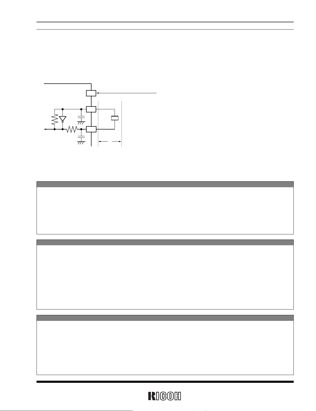
2.1 Configuration of Oscillating Circuit
Typical externally-equipped element
X'tal: 32.768kHz
(R
1=30kΩ TYP.)
(C
L=6pF to 8pF)
Standard values of internal elements
R
F=15MΩ TYP.
R
D
=120kΩ TYP.
C
G, CD=12pF TYP.
The oscillation circuit is driven at a constant voltage of approximately 1.2 volts relative to the level of the V
SS pin
input. As such, it is configured to generate an oscillating waveform with a peak-to-peak voltage on the order of 1.2
volts on the positive side of the V
SS pin input.
Considerations in Handling Crystal Oscillators
Generally, crystal oscillators have basic characteristics including an equivalent series resistance (R1)
indicating the ease of their oscillation and a load capacitance (C
L) indicating the degree of their center
frequency. Particularly, crystal oscillators intended for use with the RV5C339A is recommended to have a
typical R
1 value of 30kΩ and a typical C
L value of 6 to 8pF. To confirm these recommended values, contact
the manufacturers of crystal oscillators intended for use with these particular models.
Considerations in Installing Components around the Oscillation Circuit
1) Install the crystal oscillator in the closest possible vicinity to the real-time clock ICs.
2) Avoid laying any signal lines or power lines in the vicinity of the oscillation circuit (particularly in the area
marked “←A→” in the above figure).
3) Apply the highest possible insulation resistance between the OSCIN and OSCOUT pins and the printed
circuit board.
4) Avoid using any long parallel lines to wire the OSCIN and OSCOUT pins.
5) Take extreme care not to cause condensation, which leads to various problems such as oscillation halt.
Other Relevant Considerations
1) For external input of 32.768-kHz clock pulses to the OSCIN pin:
DC coupling: Prohibited due to an input level mismatch.
AC coupling: Permissible except that the oscillation halt sensing circuit does not guarantee perfect
operation because it may cause sensing errors due to such factors as noise.
2) To maintain stable characteristics of the crystal oscillator, avoid driving any other IC through 32.768-kHz
clock pulses output from the OSCOUT pin.
RV5C339A
VDD
10
OSCIN
9
RD
CG
CD
8
OSCOUT
R
F
32kHz
A
V
DD
Page 28

RV5C339A
28
2.2 Measurement of Oscillation Frequency
Frequency
counter
32.768kHz
OSCIN
OSCOUT
VDD
V
SS
32KOUT
RV5C339A
*
1) The RV5C339A is configured to generate 32.768-kHz clock pulses for output from the 32KOUT pin at power-on conditionally on setting the XSTP bit to
1 in the control register 2.
*
2) A frequency counter with 6 (more preferably 7) or more digits on the order of 1ppm is recommended for use in the measurement of the oscillation fre-
quency of the oscillation circuit.
*
3) The 32KOUT output pin should be connected to the VDD pin with a pull-up resistor.
2.3 Adjustment of Oscillation Frequency
The oscillation frequency of the oscillation circuit can be adjusted by varying procedures depending on the usage of
the RV5C339A in the system into which they are to be built and on the allowable degree of time count errors. The
flow chart below serves as a guide to selecting an optimum oscillation frequency adjustment procedure for the
relevant system.
Start
Use 32-kHz
clock circuit?
NO
NO
NO
YES
YES
YES
YES
NO
Use 32-kHz clock circuit without regard
to its frequency precision?
Allowable time count precision is on order of oscillation
frequency variations of crystal oscillator *
1
plus
frequency variations of real-time clock?
*
2, *3
Allowable time count precision is on order of oscillation
frequency variations of crystal oscillator
*1 plus
frequency variations of real-time clock?
*
2, *3
To Course (A)
To Course (B)
To Course (C)
To Course (D)
*
1) Generally, crystal oscillators for commercial use are classified in terms of their center frequency depending on their load capacitance (CL) and further
divided into ranks on the order of ±10, ± 20, and ±50 ppm depending on the degree of their oscillation frequency variations.
*
2) Basically, the RV5C339A are configured to cause frequency variations on the order of ±5 to ±10ppm at normal temperature.
*
3) Time count precision as referred to in the above flow chart is applicable to normal temperature and actually affected by the temperature characteristics
and other properties of crystal oscillators.
Page 29

29
RV5C339A
Course (A)
When the time count precision of each real-time clock is not to be adjusted, the crystal oscillator intended for use
with that real-time clock may have any C
L value requiring no presetting. The crystal oscillator may be subject to
frequency variations which are selectable within the allowable range of time count precision. Several crystal
oscillators and real-time clocks should be used to find the center frequency of the crystal oscillators by the method
described in “2.2 Measurement of Oscillation Frequency” and then calculate an appropriate oscillation adjustment
value by the method described in “2.4 Oscillation Adjustment Circuit” for writing this value to the RV5C339A.
Course (B)
When the time count precision of each real-time clock is to be adjusted within the oscillation frequency variations of
the crystal oscillator plus the frequency variations of the real-time clock ICs, it becomes necessary to correct
deviations in the time count of each real-time clock by the method described in “2.4 Oscillation Adjustment Circuit”.
Such oscillation adjustment provides crystal oscillators with a wider range of allowable settings of their oscillation
frequency variations and their C
L values. The real-time clock IC and the crystal oscillator intended for use with that
real-time clock IC should be used to find the center frequency of the crystal oscillator by the method described in
“2.2 Measurement of Oscillation Frequency” and then confirm the center frequency thus found to fall within the
range adjustable by the oscillation adjustment circuit before adjusting the oscillation frequency of the oscillation
circuit. At normal temperature, the oscillation frequency of the oscillator circuit can be adjusted by up to
approximately ±1.5ppm.
Course (C)
Course (C) together with Course (D) requires adjusting the time count precision of each real-time clock as well as
the frequency of 32.768-kHz clock pulses output from the 32KOUT pin. Normally, the oscillation frequency of the
crystal oscillator intended for use with the real-time clocks should be adjusted by adjusting the oscillation stabilizing
capacitors C
G and CD connected to both ends of the crystal oscillator. The RV5C339A, which incorporate the CG
and the CD, require adjusting the oscillation frequency of the crystal oscillator through its CL value.
Generally, the relationship between the C
L value and the CG and CD values can be represented by the following
equation:
CL =
C
G
× C
D
+ CS where “CS” represents the floating capacity of the printed circuit board
CG + CD
The crystal oscillator intended for use with the RV5C339A is recommended to have the CL value on the order of 6 to
8pF. Its oscillation frequency should be measured by the method described in “2.2 Measurement of Oscillation
Frequency”. Any crystal oscillator found to have an excessively high or low oscillation frequency (causing a time
count gain or loss, respectively) should be replaced with another one having a smaller and greater C
L
value,
respectively until another one having an optimum C
L value is selected. In this case, the bit settings disabling the
oscillation adjustment circuit (see “2.4 Oscillation Adjustment Circuit”) should be written to the oscillation
adjustment register.
Page 30

RV5C339A
30
2.4 Oscillation Adjustment Circuit
The oscillation adjustment circuit can be used to correct a time count gain or loss with high precision by varying the
number of 1-second clock pulses once per 20 seconds. When such oscillation adjustment is not to be made, the
oscillation adjustment circuit can be disabled by writing the settings of “
*
, 0, 0, 0, 0, 0, *” (“*” representing “0” or
“1”) to the F
6, F5, F4, F3, F2, F1, and F0 bits in the oscillation adjustment circuit. Conversely, when such oscillation
adjustment is to be made, an appropriate oscillation adjustment value can be calculated by the equation below for
writing to the oscillation adjustment circuit.
2.4-1 When Oscillation Frequency *1is Higher than Target Frequency *2(There is a Time Count Gain)
Oscillation adjustment value*3 =
(Oscillation frequency – Target frequency + 0.1)
Oscillation frequency × 3.051 × 10
–6
= (Oscillation frequency – Target frequency) × 10 + 1
*
1) Oscillation frequency: Frequency of clock pulses output from the 32KOUT pin at normal temperature in the manner described in “2.2
Measurement of Oscillation Frequency”.
*
2) Target frequency: Desired frequency to be set. Generally, a 32.768-kHz crystal oscillator has such temperature characteristics as to have
the highest oscillation frequency at normal temperature. Consequently, the crystal oscillator is recommended to have
target frequency settings on the order of 32.768 to 32.76810kHz (+3.05ppm relative to 32.768kHz). Note that the target
frequency differs depending on the environment or location where the equipment incorporating the real-time clocks is
expected to be operated.
*
3) Oscillation adjustment value: Value that is to be finally written to the F0 to F6 bits in the oscillation adjustment register and is represented in 7-bit coded
decimal notation.
*
1) The C
GOUT should have a capacitance ranging from 0 to 15pF.
Course (D)
It is necessary to select the crystal oscillator in the same manner as in Course (C) as well as correct errors in the
time count of each real-time clock in the same manner as in Course (B) by the method described in “2.4 Oscillation
Adjustment Circuit”.
10
9
8
R
F
RD
CD
CG
OSCIN
OSCOUT
32kHz
C
GOUT*
1
VDD
VDD
RV5C339A
Another advisable way to select a crystal oscillator having an optimum C
L value is to contact the manufacturer of the
crystal oscillator intended for use with the RV5C339A.
Incidentally, the high oscillation frequency of the crystal oscillator can also be adjusted by adding an external
oscillation stabilization capacitor C
GOUT as illustrated in the diagram below.
.
.
Page 31

31
RV5C339A
Notes
1) Oscillation adjustment does not affect the frequency of 32.768-kHz clock pulses output from the 32KOUT
pin.
2) Oscillation adjustment value range: When the oscillation frequency is higher than the target frequency
(causing a time count gain), an appropriate time count gain ranges from
–
3.05ppm to –189.2ppm with the
settings of “0, 0, 0, 0, 0, 1, 0” to “0, 1, 1, 1, 1, 1, 1” written to the F
6, F5, F4, F3, F2, F1, and F0 bits in the
oscillation adjustment register, thus allowing correction of a time count gain of up to +189.2ppm.
Conversely, when the oscillation frequency is lower than the target frequency (causing a time count loss),
an appropriate time count gain ranges from +3.05ppm to +189.2ppm with the settings of “1, 1, 1, 1, 1, 1, 1”
to “1, 0, 0, 0, 0, 1, 0” written to the F
6, F5, F4, F3, F2, F1, and F0 bits in the oscillation adjustment register,
thus allowing correction of a time count loss of up to
–
189.2ppm.
2.4-2 When Oscillation Frequency is Equal to Target Frequency (There is Neither a Time Count Gain
nor a Time Count Loss)
Writing the oscillation adjustment value setting of “0”, “+1”, “
–
64”, or “
–
63” to the oscillation adjustment register
disables the oscillation adjustment circuit.
2.4-3 When Oscillation Frequency is Lower than Target Frequency (There is a Time Count Loss)
Oscillation adjustment value*3 =
(Oscillation frequency – Target frequency)
Oscillation frequency × 3.051 × 10
–6
= (Oscillation frequency – Target frequency) × 10
Oscillation adjustment value calculations are exemplified below.
(1) For an oscillation frequency of 32768.85Hz and a target frequency of 32768.05Hz:
Oscillation adjustment value
=
(32768.85 – 32768.05 + 0.1) / (32768.85
×
3.051×10–6) = (32768.85 – 32768.05) ×10 + 1
= 9.001 = 9
In this instance, write the settings of “0, 0, 0, 1, 0, 0, 1” to the F
6, F5, F
4, F3, F2, F1, and F0 bits in the oscillation
adjustment register. Thus, an appropriate oscillation adjustment value in the presence of any time count gain
represents a distance from 01h.
(2) For an oscillation frequency of 32763.95Hz and a target frequency of 32768.05Hz:
Oscillation adjustment value = (32763.95 – 32768.05) / (32763.95 ×3.051 ×10–6) = (32763.95 – 32768.05) ×10
= –41.015 = –41
To represent an oscillation adjustment value of
–
41 in 7-bit coded decimal notation, subtract 41(29h) from
128(80h) to obtain 57h. In this instance, write the settings of “1, 0, 1, 0, 1, 1, 1” in the F
6, F5, F4, F3, F2, F1, and F0
bits in the oscillation adjustment register. Thus, an appropriate oscillation adjustment value in the presence of
any time count loss represents a distance from 80h.
Oscillation adjustment involves an adjustment differential of approximately ±1.5ppm from the target frequency
at normal temperature.
.
.
.
.
.
.
.
.
.
.
Page 32

RV5C339A
32
3. Oscillation Halt Sensing and Supply Voltage Monitoring
The oscillation halt sensing circuit is configured to record a halt in the oscillation of 32.768-kHz clock pulses. The
supply voltage monitoring circuit is configured to record a drop in supply voltage below a threshold voltage of 2.1 or
1.6 volts. For these functions, the real-time clock has two flag bits (i.e. the XSTP bit for the former and the VDET bit
for the latter) in which 1 is set once and this setting is maintained until 0 is written.
When the XSTP bit is set to 1 for the oscillation halt sensing circuit, the VDET bit is reset to 0 for the supply voltage
monitoring circuit. The relationship between the XSTP and VDET bits is shown in the table below.
The Oscillation halt sensing circuit operates only when the CE pin is Low. The sensing result is maintained after
the CE pin changes from “L” to “H” (See “6.4 Connection of CE Pin”).
XSTP VDET Conditions of supply voltage and oscillation
00No drop in supply voltage below threshold voltage and no halt in oscillation
01Drop in supply voltage below threshold voltage and no halt in oscillation
1
*
Halt on oscillation
When the XSTP bit is set to 1 in the control register 2, the (0), F
6 to F0, WALE, DALE, 12/24, CLEN2, TEST, CT2,
CT1, CT0, VDSL, VDET, SCRATCH, CLEN1, CTFG, WAFG, and DAFG bits are reset to 0 in the oscillation
adjustment register, the control register 1, and the control register 2. When the CE pin is “H” at power on from 0
volts, the XSTP bit is undefined, and the above bits are undefined (See “6.4 Connection of CE Pin”). Note that the
XSTP bit may be locked to 0 and the internal register broken upon instantaneous power-down.
Oscillation by 32.768-kHz clock pulses
Supply voltage monitoring (VDET)
Oscillation halt sensing (XSTP)
Normal voltage detector
Supply voltage
Internal initialization
period
(1 to 2 seconds)
Setting XSTP and
VDET bits to 0
Threshold voltage (2.1 or 1.6 volts)
Setting VDET bit to 0
Setting XSTP and
VDET bits to 0
Page 33

33
RV5C339A
< Supply Voltage Sensing Circuit >
The supply voltage monitoring circuit is configured to conduct a sampling operation during an interval of 7.8ms per
second to check for a drop in supply voltage below a threshold voltage of 2.1 or 1.6 volts for the VDSL bit setting of 0
(the default setting) or 1, respectively, in the control register 2, thus minimizing supply current requirements as
illustrated in the timing chart below. This circuit suspends a sampling operation once the VDET bit is set to 1 in the
control register 2.
7.8ms
1s
Threshold voltage
of 2.1 or 1.6 volts
Setting 0 to XSTP
and VDET bits
Setting VDET bit to 0
VDD
XSTP
Sampling operation by supply voltage
monitoring circuit
VDET
(D6 at address Fh)
Internal initialization period
(1 or 2 seconds)
Considerations in Using Oscillation Halt Sensing Circuit
Be sure to prevent the oscillation halt sensing circuit from malfunctioning by preventing the following:
1) Instantaneous power-down on the V
DD
2) Condensation on the crystal oscillator
3) On-board noise to the crystal oscillator
4) Applying to individual pins voltage exceeding their respective maximum ratings
In particular, note that the XSTP bit may fail to be set to 1 in the presence of any applied supply voltage as
illustrated below in such events as backup battery installation. Further, give special considerations to prevent
excessive chattering to power supply.
VDD
Page 34

RV5C339A
34
4. Alarm and Periodic Interrupt
The RV5C339A incorporates the alarm circuit and the periodic interrupt circuit that are configured to generate
alarm signals and periodic interrupt signals, respectively, for output from the INTRA and INTRB pins as described
below.
1)Alarm Circuit
The alarm interrupt circuit is configured to generate alarm signals for output from the INTRA or INTRB, which is
driven low (enabled) upon the occurrence of a match between current time read by the time counters (the day-of-
week, hour, and minute counters) and alarm time preset by the alarm registers (the Alarm_W registers intended
for the day-of-week, hour, and minute digit settings and the Alarm_D registers intended for the hour and minute
digit settings). The Alarm_W outputs from INTRB pin, and the Alarm_D outputs from INTRA pin.
2)Periodic Interrupt Circuit
The periodic interrupt circuit is configured to generate either clock pulses in the pulse mode or interrupt signals
in the level mode for output from the INTRA pin depending on the CT
2, CT1
, and CT0 bit settings in the control
register 1.
The above two types of interrupt signals are monitored by the flag bits (i.e. the WAFG, DAFG, and CTFG bits in the
control register 2) and enabled or disabled by the enable bits (i.e. the WALE, DALE, CT
2, CT1, and CT0 bits in the
control register 1) as listed in the table below.
Flag bits Enable bits Output pin
Alarm signals WAFG bit WALE bit
INTRB
(under control of Alarm_W registers)
(D1 at Address Fh) (D7 at Address Eh)
Alarm signals DAFG bit DALE bit
INTRA
(under control of Alarm_D registers)
(D0 at Address Fh) (D6 at Address Eh)
Periodic interrupt signals
CTFG bit CT2, CT1, and CT0 bits (D2 to D0 at Address Eh)
INTRA
(D2 at Address Fh)
(these bit settings of 0 disable the periodic interrupt circuit)
· At power-on, when the WALE, DALE, CT2, CT1, and CT0 bits are set to 0 in the control register 1, the INTRA and
INTRB pin are driven high (disabled).
· When two types of interrupt signals are output simultaneously from the INTRA pin, the output from the INTRA
pin becomes an OR waveform of their negative logic.
Alarm_D
Priodic Interrupt
INTRA
In this event, which type of interrupt signal is output from the INTRA pin can be confirmed by reading
the DAFG and CTFG bit settings in the control register 2.
Example: Combined Output of Alarm Interrupt Signals from the INTRA pin Under Control of Alarm_D and periodic
interrupt Registers
Page 35

35
RV5C339A
4.1 Alarm Interrupt
The alarm circuit is controlled by the enable bits (i.e. the WALE and DALE bits in the control register 1) and the
flag bits (i.e. the WAFG and DAFG bits in the control register 2). The enable bits can be used to enable this circuit
when set to 1 and to disable it when set to 0. When intended for reading, the flag bits can be used to monitor alarm
interrupt signals. When intended for writing, the flag bits will cause no event when set to 1 and will drive high (dis-
able) the alarm circuit when set to 0.
The enable bits will not be affected even when the flag bits are set to 0. In this event, therefore, the alarm circuit will
continue to function until it is driven low (enabled) upon the next occurrence of a match between current time and
preset alarm time.
The alarm function can be set by presetting desired alarm time in the alarm registers (the Alarm_W registers for the
day-of-week digit settings and both the Alarm_W registers and the Alarm_D registers for the hour and minute digit
settings) with the WALE and DALE bits once set to 0 and then to 1 in the control register 1. Note that the WALE
and DALE bits should be once set to 0 in order to disable the alarm circuit upon the coincidental occurrence of a
match between current time and preset alarm time in the process of setting the alarm function.
Interval (1 minute) during which
a match between current time
and preset alarm time occurs
INTRB (INTRA) pin
Setting WALE
and DALE
bit to 1
Match between
current time and
preset alarm time
in the day-of-week
and hour settings
Match between
current time and
preset alarm time
in the day-of-week
and hour settings
Match between
current time and
preset alarm time
in the day-of-week
and hour settings
Setting WALE
and DALE
bit to 0
Setting WALE
and DALE
bit to 1
Match between
current time and
preset alarm time
in the day-of-week
and hour settings
Setting WAFG
and DAFG
bit to 0
Setting WALE
and DALE
bit to 1
Setting WALE
and DALE
bit to 0
MAX.61.1µs
INTRB (INTRA) pin
Page 36

RV5C339A
36
4.2 Periodic Interrupt
Setting of the periodic selection bits (CT2 to CT0
) enables periodic interrupt from the INTRA pin to the CPU. There
are two waveform modes: pulse mode and level mode. In the pulse mode, the output has a waveform duty cycle of
around 50%. In the level mode, the output is cyclically driven low and, when the CTFG bit is set to 0, the output is set
to high (OFF).
Waveform Mode, Cycle and Falling Timing
1) Pulse Mode : 2-Hz and 1-Hz clock pulses are output in synchronization with the increment of the second counter
as illustrated in the timing chart on the next page.
2) Level Mode : periodic interrupt signals are output with selectable interrupt cycle settings of 1 second, 1 minute, 1
hour, and 1 month. The increment of the second counter is synchronized with the falling edge of
periodic interrupt signals. For example, periodic interrupt signals with an interrupt cycle setting of
1 second are output in synchronization with the increment of the second counter as illustrated in
the timing chart on the next page.
3) When the oscillation adjustment circuit is used, the interrupt cycle will fluctuate once per 20 seconds as follows:
Pulse Mode : the “L” period of output pulses will increment or decrement by a maximum of ±3.784ms.
For example, 1-Hz clock pulses will have a duty cycle of 50 ±0.3784%.
Level Mode : a periodic interrupt cycle of 1 second will increment or decrement by a maximum of ±3.784ms.
CT2 CT1 CT
0
Description
Waveform mode
Cycle and falling timing
000—Off (“H”)
001—Fixed at low (“L”)
010
Pulse Mode
*
1
2Hz (Duty cycle of 50%)
011
Pulse Mode
*
1
1Hz (Duty cycle of 50%)
100
Level Mode
*
2
Once per 1 second (Synchronized with second counter increment)
101
Level Mode
*
2
Once per minute (at 00 seconds of every minute)
110
Level Mode
*
2
Once per hour (at 00 minutes and 00 seconds of every hour)
111
Level Mode
*
2
Once per month (at 00 hours, 00 minutes, and 00 seconds of first day of every month)
(Default setting)
Page 37

37
RV5C339A
Approx. 92µs
CTFG bit
INTRA pin
(Increment of second counter)
Rewriting of the second counter
Relation Between the Mode Waveform and the CTFG Bit
• Pulse mode
*
) In the pulse mode, the increment of the second counter is delayed by approximately 92 µs from the falling edge of clock pulses. Consequently, time
readings immediately after the falling edge of clock pulses may appear to lag behind the time counts of the real-time clocks by approximately 1 second.
Rewriting the second counter will reset the other time counters of less than 1 second, driving the INTRA pin low.
Setting CTFG bit to 0
(Increment of
second counter)
Setting CTFG bit to 0
CTFG bit
INTRA pin
(Increment of
second counter)
(Increment of
second counter)
5. 32-kHz Clock Output
32.768-kHz clock pulses are output from the 32KOUT pin when either the CLEN1 bit in the control register 2 or the
CLEN2 bit in the control register 1 is set to 0. If the conditions described above are not satisfied, the output is set to
high.
CLEN1 CLEN2
32KOUT pin output
(D3 at Address Fh) (D4 at Address Eh) (Nch Open Drain output)
11Off (“H”)
0 (Default)
*
Clock pulses
*
0 (Default)
The 32KOUT pin output is synchronized with the CLEN1 or CLEN2 bit, settings as illustrated in the timing chart
below.
MAX. 61.0µs MAX. 45.8µs
32KOUT pin
CLEN1 or CLEN2
• Level mode
Page 38

RV5C339A
38
6. Typical Applications
6.1 Typical Power Circuit Configurations
Sample circuit configuration 1
System power supply
RV5C339A
32.768kHz
OSCIN
OSCOUT
VDD
VSS
*
1
Sample circuit configuration 2
System power supply
RV5C339A
OSCIN
OSCOUT
VDD
VSS
32.768kHz
*
1
*
1) Install bypass capacitors for high-frequency and low-
frequency applications in parallel in close vicinity to the
RV5C339A.
*
1) When using an OR diode as a power supply for the
RV5C339A , ensure that voltage exceeding the absolute
maximum rating of V
DD+0.3 volts is not applied the SIO pin.
Page 39

39
RV5C339A
6.2 Connection of INTRA and INTRB Pins
The INTRA and INTRB pins follow the N-channel open drain output logic and contain no protective diode on the
power supply side. As such, it can be connected to a pull-up resistor of up to 5.5 volts regardless of supply voltage.
6.3 Connection of 32KOUT Pin
The 32KOUT pin follows the Nch. open drain output and contains no protective diode on the power supply side. As
such, it can be connected to a device with a supply voltage of up to 5.5 volts regardless of supply voltage, provided
that such connection involves considerations for the supply current requirements of a pull-up resistor, which can be
roughly calculated by the following equation:
I=0.5
×(V
DD or VCC
)/Rp
System power supply
A
B
OSCIN
OSCOUT
VDD
VSS
INTRA or INTRB
Backup battery
32.768kHz
RV5C339A
*
1
OSCIN
OSCOUT
VDD
VSS
32KOUT
System power supply (VCC)
A
B
Backup battery
32.768kHz
Rp
(V
DD)
RV5C339A
*
1
*
1) Depending on whether the INTRA and INTRB pins are to be
used during battery backup, it should be connected to a pull-up
resistor at the following different positions:
1) Position A in the left diagram when it is not to be used during
battery backup.
2) Position B in the left diagram when it is to be used during
battery backup.
*
1) Depending on whether the 32KOUT pin is to be used during
battery backup, it should be connected to a pull-up resistor at
the following different positions:
1) Position A in the left diagram when it is not to be used during
battery backup.
2) Position B in the left diagram when it is to be used during
battery backup.
Page 40

RV5C339A
40
6.4 Connection of CE Pin
Observe the following precautions when you connect the CE pin.
1) The CE pin is configured to enable the oscillation halt sensing circuit only when driven low. As such, it should be
driven low or open at power-on from 0 volts.
2) The CE pin should also be driven low or open immediately upon the host going down (see “1.5 Considerations in
Reading and Writing Time Count Data”).
3) The reading function should be disrupted when the CE signal goes to “low” during read cycle. While, the upper 4
bits of the data might be written to the inner shift register when the CE signal goes to “low” during write cycle.
(Because the writing function is executed 4 bits by 4 bits.) In either case, after the CE signal returns to “High”,
no trouble will occur in the next read or write cycle.
I/O
CONTROL
SCLK
SIO
CE
2
3
7
Lower limit operating voltage
for the CPU
Backup voltage
0.2×V
DD
MIN. 0µs MIN. 0µs MIN. 0µs
V
DD
CE
Page 41

41
RV5C339A
X'tal : 32.768kHz
(R
1=30kΩ TYP.)
(C
L
=6pF to 8pF)
Topt : 25˚C
Output pins : Open
Frequency
counter
32.768kHz
OSCIN
OSCOUT
VDD
V
SS
32KOUT
RV5C339A
7.1 Timekeeping Current vs. Supply Voltage
(with no 32-kHz clock output)
01 34562
1
0.8
0.6
0.4
0.2
0
Timekeeping Current IDD(µA)
Supply Voltage VDD(V)
(CE=Open, Output=Open, Topt=25˚C)
01 34 5 62
3
2.5
2
1.5
0.5
0
Timekeeping Current IDD(µA)
Supply Voltage VDD(V)
1
(CE=Open, Output=Open, Topt=25˚C)
7.3 CPU Access Current vs. SCLK Clock Frequency
0 500 1000 1500
2000
50
40
30
20
10
0
CPU Access Current IDD(µA)
SCLK Clock Frequency (kHz)
VDD=5V
VDD=3V
(Output=Open, Topt=25˚C)
–60 –40 20 40 60 100–20
2
1.5
0.5
0
Timekeeping Current IDD(µA)
Operating Temperature Topt(˚C)
1
080
(CE=Open, Output=Open)
7. Typical Characteristics
• Test Circuit
7.2 Timekeeping Current vs. Supply Voltage
(with 32-kHz clock output)
7.4 Timekeeping Current vs. Operating Temperature
(with no 32-kHz clock output)
Page 42
RV5C339A
42
7.5 Oscillation Frequency Deviation vs. External C
G
051015 20
10
5
0
–5
–10
–15
–20
–25
–30
–35
–40
Oscillation Frequency Deviation(ppm)
External CG(pF)
(VDD=3V, Topt=25˚C,
External C
G=0pF as standard)
7.6 Oscillation Frequency Deviation vs. Supply Voltage
Oscillation Frequency Deviation(ppm)
5
4
3
2
1
0
–1
–2
–3
–4
–5
0123456
Supply Voltage VDD(V)
(Topt=25˚C, VDD=3V as standard)
7.7 Oscillation Frequency Deviation vs.
Operating Temperature
Oscillation Frequency Deviation(ppm)
–60 –40 –20 0 20 40 60 80 100
20
0
–20
–40
–60
–80
–100
–120
–140
Operating Temperature Topt(˚C)
(VDD=3V, Topt=25˚C as standard)
Oscillation Start Time(ms)
Supply Voltage VDD(V)
500
400
300
200
100
0
0123456
(Topt=25˚C)
7.9 VOL
vs. IOL (INTRA, INTRB, 32KOUT Pin)
VDD=5V
30
25
20
15
10
5
0
0 1.00.2 0.4 0.6 0.8
VOL (V)
IOL (mA)
VDD=3V
(Topt=25˚C)
7.8 Oscillation Start Time vs. Supply Voltage
Page 43

43
RV5C339A
8. Typical Software-based Operations
8.1 Initialization at Power-on
Start
XSTP=1?
Power-on
NO
NO
YES
YES
Warning of Backup Battery
Run-down
VDET=0?
*
1
*
2
*
4
*
3
Set Oscillation Adjustment Register
and Control Registers 1 and 2, etc.
8.2 Writing of Time and Calendar Data
Wait for 31µs
Write to Time Counter
and Calendar Counter
*
1
*
2
*
1) After power-on from 0 volts, the start of oscillation and the process of internal initialization require a time span on the order of 1 to 2 seconds, so that
access should be done after the lapse of this time span or more.
*
2) The XSTP bit setting of 0 in the control register 1 indicates power-on from backup battery and not from 0 volt. The XSTP bit may fail to be set to 1 in the
presence of any excessive chattering in power supply in such events as installing backup battery. Should there be any possibility of this failure occurring,
it is recommended to initialize the RV5C339A regardless of the current XSTP bit setting. For further details, see “3. Oscillation Halt Sensing and Supply
Voltage Monitoring”.
*
3) This step is not required when the supply voltage monitoring circuit is not used.
*
4) This step involves ordinary initialization including the oscillation adjustment register and interrupt cycle settings.
*
1) This step of waiting is detailed in “1.5 Considerations in Reading
and Writing Time Data”.
*
2) Any writing to the second counter will reset divider units lower than
the second digits.
The RV5C339A may also be initialized not at power-on but in the
process of writing time and calender data.
Page 44

RV5C339A
44
8.3 Reading Time and Calendar Data
8.3-1 Ordinary Process of Reading Time and Calendar Data
Wait for 31µs
Read from Time Counter
and Calendar Counter
*
1
8.3-2 Basic Process of Reading Time and Calendar Data Synchronized with Periodic Interrupt
CTFG=1?
Other Interrupt
Processes
Generate Interrupt in CPU
Write “×,1,×,1,×,0,1,1”
to Control Register 2
Set Periodic Interrupt
Cycle Selection Bits
YES
NO
Read from Time Counter
and Calendar Counter
*
1
*
2
*
3
*
1) This step of waiting is detailed in “1.5 Considerations in Reading and
Writing Time Data”.
*
1) This step is intended to select the level mode as a waveform mode for the
periodic interrupt function.
*
2) If this step is completed within 1 second, the step of waiting described in
“8.3-1 Ordinary Process of Reading Time and Calendar Data” above need
not be conducted. This step is detailed in “1.5 Considerations in Reading
and Writing Time Data”.
*
3) This step is intended to set the CTFG bit to 0 in the control register 2 to
cancel an interrupt to the CPU.
Page 45
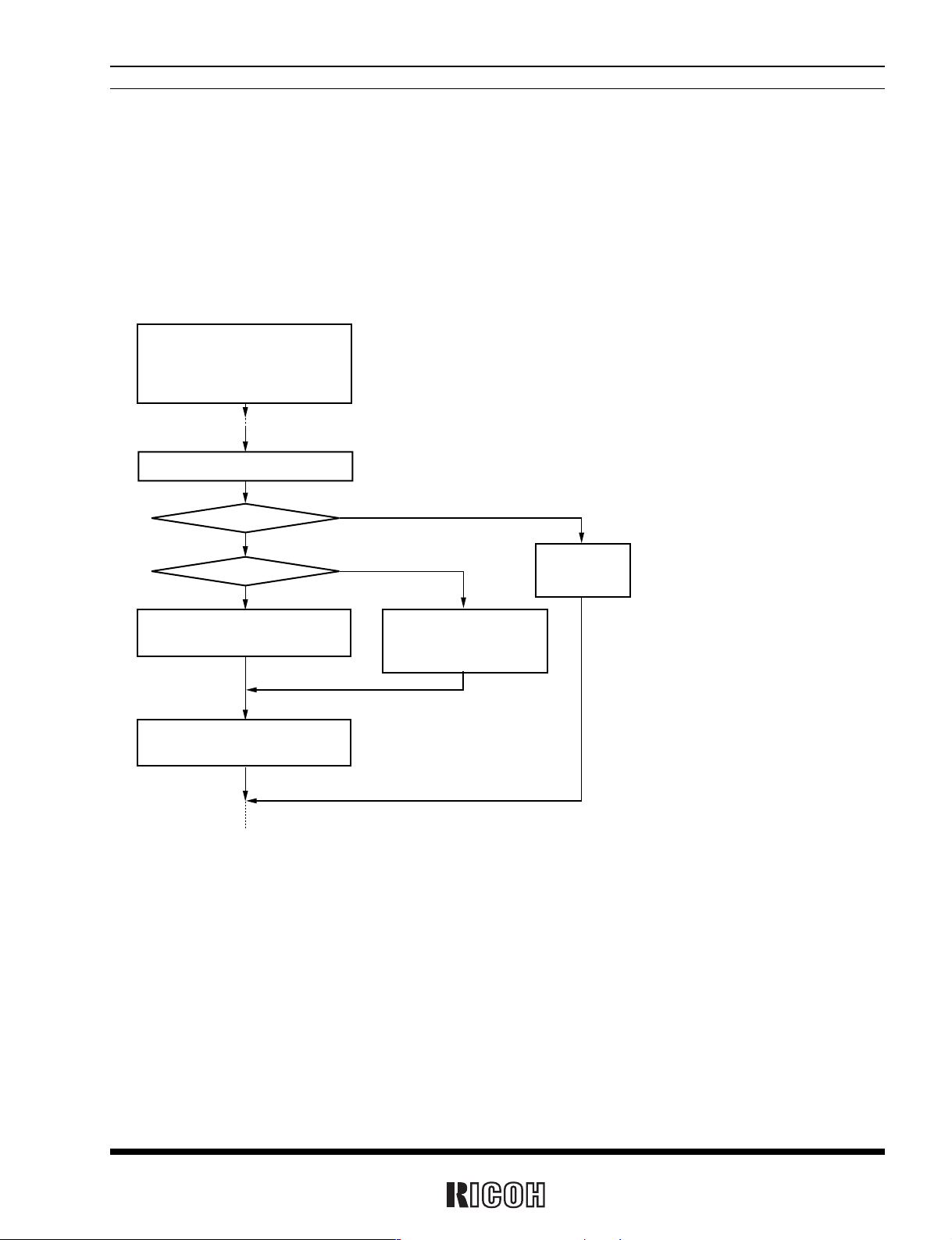
45
RV5C339A
8.3-3 Applied Process of Reading Time and Calendar Data Synchronized with Periodic Interrupt Function
Time data need not be read from all the time counters when used for such ordinary purposes as time count
indication. This applied process can be used to read time and calendar data with substantial reductions in the load
involved in such reading.
CTFG=1?
Generate Interrupt to CPU
Write “×,×,×,×,0,1,0,0”
to control Register 1
Write “×,1,×,1,×,0,1,1”
to Control Register 2
NO
YES
Second Digit=00?
NO
YES
Use Previous Minute,
Hour, Day-of-week,
and Day-of-month Data
Read Minute, Hour, Day-of-week,
and Day-of-month Counters
*
1
*
2
*
4
*
3
Other Interrupt
Processes
Write “×,1,×,1,×,0,1,1”
to Control Register 2
For Time Indication in “Day-of-month, Day-of-week, Hour,
Minute, and Second” Format:
*
1) This step is intended to select the level mode as a waveform mode for the periodic interrupt function.
*
2) If this step is completed within 1 second, the step of waiting described in “8.3-1 Ordinary Process of Reading Time and Calendar Data” above need not be
conducted. This step is detailed in “1.5 Considerations in Reading and Writing Time Data”.
*
3) This step is intended to read time data from all the time counters only in the first session of reading time data after writing time data.
*
4) This step is intended to set the CTFG bit to 0 in the control register 2 to cancel an interrupt to the CPU.
Page 46
RV5C339A
46
YES
NO
Periodic Interrupt Process
CTFG=1?
Other Interrupt
Processes
Generate Interrupt to CPU
Write “×,1,×,1,×,0,1,1”
to Control Register 2
Set Periodic Interrupt
Cycle Selection Bits
*
1
*
2
WAFG or DAFG=1?
Generate Interrupt to CPU
WALE or DALE=1
YES
NO
Conduct Alarm Interrupt
WALE or DALE=0
Set Alarm Minute, Hour,
and Day-of-week Registers
Other Interrupt
Processes
Write “×,1,×,1,×,1,0,1”
to Control Register 2
*
1
*
2
*
3
8.4-2 Alarm Interrupt
8.4 Interrupt Process
8.4-1 Periodic Interrupt
*
1) This step is intended to select the level mode as a waveform mode for the
periodic interrupt function.
*
2) This step is intended to set the CTFG bit to 0 in the control register 2 to
cancel an interrupt to the CPU.
*
1) This step is intended to once disable the alarm interrupt circuit by setting
the WALE and DALE bits to 0 in anticipation of the coincidental occurrence
of a match between current time and preset alarm time in the process of
setting the alarm interrupt function.
*
2) This step is intended to enable the alarm interrupt function after completion
of all alarm interrupt settings.
*
3) This step is intended to once cancel the alarm interrupt function by writing
the settings of “×,1,×,1,×,1,0,1” and “×,1,×,1,×,1,1,0” to the Alarm_W
registers and the Alarm_D registers, respectively.
 Loading...