

RICOH RV5C338A Datasheet

3-WIRE SERIAL INTERFACE REAL-TIME CLOCK IC
S
WITH VOLTAGE MONITORING FUNCTION
R×5C338A
ELECTRONIC DEVICES DIVISION
NO.EA-053-9908
APPLICATION MANUAL

NOTICE
1. The products and the product specifications described in this application manual are subject to change or
discontinuation of production without notice for reasons such as improvement. Therefore, before deciding to
use the products, please refer to Ricoh sales representatives for the latest information thereon.
2. This application manual may not be copied or otherwise reproduced in whole or in part without prior written
consent of Ricoh.
3. Please be sure to take any necessary formalities under relevant laws or regulations before exporting or
otherwise taking out of your country the products or the technical information described herein.
4. The technical information described in this application manual shows typical characteristics of and example
application circuits for the products. The release of such information is not to be construed as a warranty of or a
grant of license under Ricoh's or any third party's intellectual property rights or any other rights.
5. The products listed in this document are intended and designed for use as general electronic components in
standard applications (office equipment, computer equipment, measuring instruments, consumer electronic
products, amusement equipment etc.). Those customers intending to use a product in an application requiring
extreme quality and reliability, for example, in a highly specific application where the failure or misoperation of
the product could result in human injury or death (aircraft, spacevehicle, nuclear reactor control system, traffic
control system, automotive and transportation equipment, combustion equipment, safety devices, life support
system etc.) should first contact us.
6. We are making our continuous effort to improve the quality and reliability of our products, but semiconductor
products are likely to fail with certain probability. In order prevent any injury to persons or damages to property
resulting from such failure, customers should be careful enough to incorporate safety measures in their design,
such as redundancy feature, fire-containment feature and fail-safe feature. We do not assume any liability or
responsibility for any loss or damage arising from misuse or inappropriate use of the products.
7. Anti-radiation design is not implemented in the products described in this application manual.
8. Please contact Ricoh sales representatives should you have any questions or comments concerning the
products or the technical information.
June 1995

OUTLINE
......................................................................................................
1
FEATURES
....................................................................................................
1
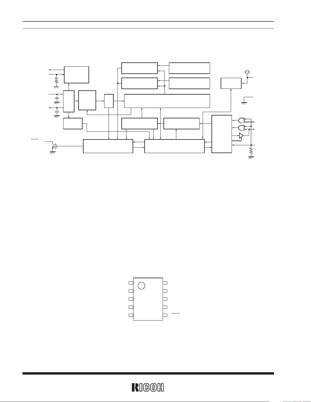
BLOCK DIAGRAM
.........................................................................................
2
APPLICATIONS
.............................................................................................
2
PIN CONFIGURATION
...................................................................................
2
PIN DESCRIPTIONS
......................................................................................
3
ABSOLUTE MAXIMUM RATINGS
...................................................................
4
RECOMMENDED OPERATING CONDITIONS
.................................................
4
DC ELECTRICAL CHARACTERISTICS
...........................................................
5
AC ELECTRICAL CHARACTERISTICS
...........................................................
6
GENERAL DESCRIPTION
..............................................................................
7
FUNCTIONAL DESCRIPTIONS
......................................................................
9
1. Address Mapping
.........................................................................................
9
2. Register Settings
.......................................................................................
10
USAGES
......................................................................................................
21
1. Data Transfer Formats
..................................................................................
21
2. Configuration of Oscillation Circuit and Correction of Time Count Deviations
...................
27
3. Oscillation Halt Sensing and Supply Voltage Monitoring
...........................................
32
4. Alarm and Periodic Interrupt
...........................................................................
34
5. 32-kHz Clock Output
....................................................................................
37
6. Typical Applications
.....................................................................................
38
7. Typical Characteristics
..................................................................................
41
8. Typical Software-based Operations
...................................................................
43
PACKAGE DIMENSIONS
..............................................................................
47
TAPING SPECIFICATIONS
...........................................................................
48
R×5C338A
APPLICATION MANUAL
CONTENTS

1
3-WIRE SERIAL INTERFACE REAL-TIME CLOCK ICS
WITH VOLTAGE MONITORING FUNCTION
R×5C338A
OUTLINE
The R×5C338A are CMOS real-time clock ICs connected to the CPU by three signal lines CE (Chip Enable), SCLK
(Serial Clock), and SIO (Serial Input/Output), and configured to perform serial transmission of time and calendar
data to the CPU. These models incorporate different functional circuits. The periodic interrupt circuit is configured
to generate interrupt signals with six selectable interrupts ranging from 0.5 seconds to 1 month. The 2 alarm
circuits generate interrupt signals at preset times. The oscillation circuit is driven under constant voltage so that
fluctuations in oscillation frequency due to voltage are small and supply current is also small (TYP. 0.35µA at 3
volts). The oscillation halt sensing circuit can be used to judge the validity of internal data in such events as poweron. The supply voltage monitoring circuit is configured to record a drop in supply voltage below two selectable
supply voltage monitoring threshold settings. The 32-kHz clock output function is intended to output sub-clock
pulses for the external microcomputer. The oscillation adjustment circuit is intended to adjust time counts with
high precision by correcting deviations in the oscillation frequency of the crystal oscillator. These models come in
an ultra-compact 10-pin SSOP (RS5C338A with a height of 1.25mm and a pin pitch of 0.5mm)and 10-pin SSOP-G
(RV5C338A with a height of 1.2mm and a pin pitch of 0.5mm).
FEATURES
• Timekeeping supply voltage ranging from 1.45 to 5.5 volts
• Low supply current: TYP. 0.35µA (MAX. 0.8µA) at 3 volts (at 25˚C)
• Only three signal lines (SCLK, SIO, and CE) required for connection to the CPU.
Maximum clock frequency of 2 MHz (with V
DD of 5 volts)
• Time counters (counting hours, minutes, and seconds) and calendar counters (counting years, months, days, and
weeks) (in BCD format)
• 1900/2000 identification bit for Year 2000 compliance
• Interrupt circuit configured to generate interrupt signals (with interrupts ranging from 0.5 seconds to 1 month) to
the CPU and provided with an interrupt flag and an interrupt halt circuit
• 2 alarm circuits (Alarm_W for week , hour , and minute alarm settings and Alarm_D for hour and minute alarm
settings)
• 32-kHz clock circuit (CMOS output, equipped with a control pin)
• Oscillation halt sensing circuit which can be used to judge the validity of internal data
• Supply voltage monitoring circuit with two supply voltage monitoring threshold settings
• Automatic identification of leap years up to the year 2099
• Selectable 12-hour and 24-hour mode settings • Built-in oscillation stabilization capacitors (C
G and CD)
• High precision oscillation adjustment circuit • CMOS process
• Ultra-compact 10-pin SSOP (RS5C338A with a height of 1.25mm and size of 6.4
×3.5mm)
Ultra-compact 10-pin SSOP-G (RV5C338A with a height of 1.20mm and size of 4.0
×2.9mm)
R×5C338A
2
BLOCK DIAGRAM
COMPARATOR_W
ALARM_W REGISTER
(MIN,HOUR,WEEK)
ALARM_D REGISTER
(MIN,HOUR)
COMPARATOR_D
TIME COUNTER
(SEC,MIN,HOUR,WEEK,DAY,MONTH,YEAR)
ADDRESS
REGISTER
ADDRESS
DECODER
SHIFT REGISTER
INTERRUPT CONTROL
32kHz
OUTPUT
CONTROL
DIVIDER
CORREC
-TION
DIVOSC
OSCIN
32KOUT
CLKC
OSCOUT
OSC
DETECT
I/O
CONTROL
VSS
SCLK
SIO
CE
VDD
INTR
VOLTAGE
DETECT
PIN CONFIGURATION
32KOUT
1
SCLK
2
SIO
3
VSS
CE
VDD
OSCIN
OSCOUT
CLKC
INTR
4
5
8
9
10
7
6
• 10-pin SSOP-G, 10-pin SSOP
APPLICATIONS
• Communication devices (multi function phone, portable phone, PHS or pager)
• OA devices (fax, portable fax)
• Computer (desk-top and mobile PC, portable word-processor, PDA, electric note or video game)
• AV components (portable audio unit, video camera,camera, digital camera or remote controller)
• Home appliances (rice cooker, electric oven)
• Other (car navigation system, multi-function watch)
3
R×5C338A
PIN DESCRIPTIONS
Pin No.
Symbol Name Description
4 CE Chip Enable Input
The CE pin is used for interfacing with the CPU. Should be held high to allow
access to the CPU. Incorporates a pull-down resistor. Should be held low or open
when the CPU is powered off. Allows a maximum input voltage of 5.5 volts regardless of supply voltage.
2 SCLK Serial Clock Input
The SCLK pin is used to input clock pulses synchronizing the input and output of
data to and from the SIO pin. Allows a maximum input voltage of 5.5 volts regardless of supply voltage.
3 SIO Serial Input/Output
The SIO pin is used to input and output data intended for writing and reading in
synchronization with the SCLK pin. CMOS input/output.
6 INTR Interrupt Output
The INTR pin is used to output periodic interrupt signals to the CPU and alarm
interrupt signals (Alarm_W, Alarm_D). Disabled at power-on from 0 volts.
Nch. open drain output.
1 32KOUT
32-kHz Clock Output
The 32KOUT pin is used to output 32.768-kHz clock pulses. Enabled at power-on
from 0 volts. CMOS output. This pin is disabled if the CLKC pin is set to low or
open.
7 CLKC Clock Control Input
The CLCK pin is used to control output of the 32KOUT pin. The clock output is
disabled and held low when the pin is set to low or open. Incorporates a pull-down
resistor.
The OSCIN and OSCOUT pins are used to connect the 32.768-kHz crystal oscilla-
tor (with all other oscillation circuit components built into the R×5C338A.)
The VDD pin is connected to the power supply. The VSS pin is grounded.
9 OSCIN Oscillation Circuit
8
OSCOUT
Input/Output
10 VDD
Positive Power Supply Input
5 VSS
Negative Power Supply Input
R×5C338A
4
RECOMMENDED OPERATING CONDITIONS
(Vss=0V,Topt=–40 to +85˚C)
Symbol Item Conditions MIN. TYP. MAX. Unit
VDD Supply Voltage 2.0 5.5 V
VCLK Timekeeping Voltage 1.45 5.5 V
fXT Oscillation Frequency 32.768 kHz
V
PUP Pull-up Voltage INTR 5.5 V
ABSOLUTE MAXIMUM RATINGS
Absolute Maximum ratings are threshold limit values that must not be exceeded even for an instant under
any conditions. Moreover, such values for any two items must not be reached simultaneously. Operation
above these absolute maximum ratings may cause degradation or permanent damage to the device. These
are stress ratings only and do not necessarily imply functional operation below these limits.
ABSOLUTE MAXIMUM RATINGS
Symbol Item Conditions Ratings Unit
VDD Supply Voltage –0.3 to +6.5 V
VI
Input Voltage 1 SIO –0.3 to VDD+0.3
V
Input Voltage 2 SCLK, CE,CLKC –0.3 to +6.5
VO
Output Voltage 1 SIO, 32KOUT –0.3 to VDD+0.3
V
Output Voltage 2 INTR –0.3 to +6.5
PD Power Dissipation Topt=25˚C 300 mW
Topt Operating Temperature –40 to +85 ˚C
Tstg Storage Temperature –55 to +125 ˚C
(Vss=0V)
5
R×5C338A
DC ELECTRICAL CHARACTERISTICS
Symbol Item Pin name Conditions MIN. TYP. MAX. Unit
VIH1 “H” Input Voltage SCLK,CE,CLKC 0.8VDD 5.5
V
IH2 “H” Input Voltage SIO VDD=2.5 to 5.5V 0.8VDD
VDD+0.3
V
VIL “L” Input Voltage SCLK,CE,SIO,CLKC –0.3 0.2VDD
IOH “H” Output Current SIO,32KOUT VOH=VDD–0.5V –0.5 mA
I
OL1
”L” Output Current
INTR
VOL=0.4V 2
mA
IOL2 SIO,32KOUT VOL=0.4V 0.5
I
IL Input Leakage Current SCLK
V
I=5.5V or Vss
–1 1 µA
VDD=5.5V
RDNCE Pull-down Resistance CE 40 120 400 kΩ
I
CLKC
Pull-down Resistance
CLKC 0.35 1.0 µA
Input Current
I
OZ1
Output Off-state
SIO
Vo=5.5V or Vss
–1 1
µA
Leakage Current
V
DD=5.5V
IOZ2 INTR VO=5.5V –1 1
VDD=3V,CE=OPEN
IDD1 Standby Current VDD Output=OPEN 0.35 0.8 µA
32KOUT=Off mode*
1
VDETH
Supply Voltage Monitoring
VDD Topt=–30 to +70˚C 1.90 2.10 2.30 V
Voltage (“H”)
VDETL
Supply Voltage Monitoring
VDD Topt=–30 to +70˚C 1.45 1.60 1.80 V
Voltage (“L”)
CG
Internal Oscillation Capacitance 1
OSCIN 12
pF
C
D
Internal Oscillation Capacitance 2
OSCOUT 12
Unless otherwise specified: Vss=0V,VDD=3V,Topt=–40 to +85˚C
*
1) For standby current for outputting 32.768-kHz clock pulses from the 32KOUT pin, see “USAGES, 7. Typical Characteristics”.
R×5C338A
6
Symbol Item Conditions
V
DD≥2.5V VDD≥4.5
Unit
MIN. TYP. MAX. MIN. TYP. MAX.
tCES CE Set-up Time 400 200 ns
tCEH CE Hold Time 400 200 ns
tCR CE Recovery Time 62 62 µs
fSCLK SCLK Clock Frequency 1.0 2.0 MHz
tCKH SCLK Clock “H” Time 400 200 ns
tCKL SCLK Clock “L” Time 400 200 ns
tCKS SCLK Set-up Time 200 100 ns
tRD Data Output Delay Time 300 150 ns
tRZ Data Output Floating Time 300 150 ns
tCEZ
Data Output Floating Time
300 150 ns
After Falling of CE
tDS Input Data Set-up Time 200 100 ns
tDH Input Data Hold Time 200 100 ns
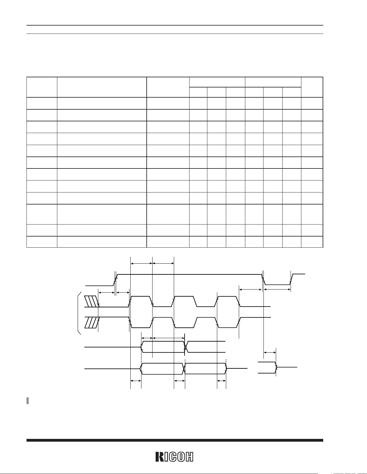
AC ELECTRICAL CHARACTERISTICS
Unless otherwisespecified : Vss=0V, Topt=–40 to +85˚C
Input/output conditions : V
IH=0.8 × VDD, VIL=0.2 × VDD, VOH=0.8 × VDD, VOL=0.2 ×VDD, CL=50pF
CE
SCLK
SIO (Write cycle)
SIO (Read cycle)
tCKH tCKL
tCKS
tCES
tDS tDH
tRD
tRD tRZ
tCEZ
tCEH
tCR
*
) For read/write timing, see Paragraph “USAGES, 1.5 Considerations in Reading and Writing Time Data”

7
R×5C338A
GENERAL DESCRIPTION
1. Interface with CPU
The R×5C338A are connected to the CPU by three signal lines CE (Chip Enable), SCLK (Serial Clock), SIO (Serial
Input/Output), through which it reads and write data from and to the CPU. The CPU can access when the CE pin is
held high. Access clock pulses have a maximum frequency of 2MHz (at 5 volts), allowing high-speed data transfer
to the CPU.
2. Clock and Calendar Function
The R×5C338A read and write time data from and to the CPU in units ranging from seconds to the last two digits of
the calendar year. The calendar year will automatically be identified as a leap year when its last two digits are a multiple of 4. Also available is the 1900/2000 identification bit for Year 2000 compliance. Consequently, leap years up to
the year 2099 can automatically be identified as such.
*
) The year 2000 is a leap year while the year 2100 is not a leap year.
3. Alarm Function
The R×5C338A incorporate an alarm circuit configured to generate interrupt signals to the CPU for output at preset
times. The alarm circuit allows two types of alarm settings specified by the Alarm_W registers and the Alarm_D
registers. The Alarm_W registers allow week, hour, and minute alarm settings including combinations of multiple
day-of-week settings such as “Monday, Wednesday, and Friday” and “Saturday and Sunday”. The Alarm_D registers allow hour and minute alarm settings. Both Alarm_W and Alarm_D signals are output from the INTR pin. The
current alarm settings specified by these two registers can be checked from the CPU by using a polling function..
4. High-precision Oscillation Adjustment Function
The R×5C338A have built-in oscillation stabilization capacitors (CG and CD), which can be connected to an external
crystal oscillator to configure an oscillation circuit. To correct deviations in the oscillation frequency of the crystal
oscillator, the oscillation adjustment circuit is configured to allow correction of a time count gain or loss (up to ±1.5
ppm at 25˚C) from the CPU within a maximum range of approximately ±189 ppm in increments of approximately 3
ppm. Such oscillation frequency adjustment in each system has the following advantages:
· Allows timekeeping with much higher precision than conventional real-time clocks while using a crystal oscillator
with a wide range of precision variations.
· Corrects seasonal frequency deviations through seasonal oscillation adjustment.
· Allows timekeeping with higher precision particularly in systems with a temperature sensing function through
oscillation adjustment in tune with temperature fluctuations.

R×5C338A
8
5. Oscillation Halt Sensing Function and Supply Voltage Monitoring Function
The R×5C338A incorporate an oscillation halt sensing circuit equipped with internal registers configured to record
any past oscillation halt, thereby identifying whether they are powered on from 0 volts or battery backed-up. As
such, the oscillation halt sensing circuit is useful for judging the validity of time data.
The R
×5C338A also incorporate a supply voltage monitoring circuit equipped with internal registers configured to
record any drop in supply voltage below a certain threshold value. Supply voltage monitoring threshold settings can
be selected between 2.1 and 1.6 volts through internal register settings.
The oscillation halt sensing circuit is configured to confirm the established invalidation of time data in contrast to
the supply voltage monitoring circuit intended to confirm the potential invalidation of time data. Further, the supply
voltage monitoring circuit can be applied to battery supply voltage monitoring.
6. Periodic Interrupt Function
The R×5C338A incorporate a periodic interrupt circuit configured to generate periodic interrupt signals aside from
interrupt signals generated by the alarm circuit for output from the INTR pin. Periodic interrupt signals have five
selectable frequency settings of 2Hz (once per 0.5 seconds), 1Hz (once per 1 second), 1/60Hz (once per 1 minute),
1/3600Hz (once per 1 hour), and monthly (the first day of every month). Further, periodic interrupt signals also
have two selectable waveforms of a normal pulse form (with a frequency of 2Hz or 1Hz) and special form adapted to
interruption from the CPU in the level mode (with second, minute, hour, and month interrupts). The register
records of periodic interrupt signals can be monitored by using a polling function.
7. 32-kHz Clock Output Function
The R×5C338A incorporate a 32-kHz clock circuit configured to generate clock pulses with the oscillation frequency
of a 32.768-kHz crystal oscillator for output from the 32KOUT pin. The 32KOUT pin is CMOS output and the output
from this pin is enabled and disabled when the CLKC pin is held high, and low or open, respectively. The 32-kHz
clock output can be disabled by certain register settings. But it cannot be disabled without manipulation of any two
registers with different addresses, to prevent disabling in such events as the runaway of the CPU. The 32-kHz clock
circuit is enabled at power-on, when the CLKC pin is held high.
9
R×5C338A
Data*
1
0 0 0 0 0 Second Counter –*
2
S40 S20 S10 S8 S4 S2 S1
1 0 0 0 1 Minute Counter – M40 M20 M10 M8 M4 M2 M1
2 0 0 1 0
Hour Counter
– –
H
20
H10 H8 H4 H2 H1
P/A
3 0 0 1 1 Day-of-week Counter – – – – – W4 W2 W1
4 0 1 0 0 Day-of-month Counter – – D20 D10 D8 D4 D2 D1
5 0 1 0 1
Month Counter and Century Bit
19/20 – – MO10 MO8 MO4 MO2 MO1
6 0 1 1 0 Year Counter Y80 Y40 Y20 Y10 Y8 Y4 Y2 Y1
7 0 1 1 1
Oscillation Adjustment Register
*
3
(0)*4F6 F5 F4 F3 F2 F1 F0
8 1 0 0 0
Alarm_W (minute register)
– WM40 WM20 WM10 WM8 WM4 WM2 WM1
9 1 0 0 1 Alarm_W (hour register) – –
WH
20
WH10 WH8 WH4 WH2 WH1
WP/A
A 1 0 1 0
Alarm_W
(day-of-week register)
– WW6 WW5 WW4 WW3 WW2 WW1 WW0
B 1 0 1 1 Alarm_D (minute register) – DM40 DM20 DM10 DM8 DM4 DM2 DM1
C 1 1 0 0 Alarm_D (hour register) – –
DH
20
DH10 DH8 DH4 DH2 DH1
DP/A
D 1 1 0 1 – – – – – – – –
E 1 1 1 0 Control Register 1
*
3
WALE DALE 12/24
CLEN2
TEST CT2 CT1 CT0
F 1 1 1 1 Control Register 2*
3
VDSL VDET
SCRATCH
XSTP
CLEN1
CTFG WAFG DAFG
D3 D2
D1
D0
Address
A3
A2 A1 A0
Register
D4D5D6D7
FUNCTIONAL DESCRIPTIONS
1. Address Mapping
*
1) All the data listed above accept both reading and writing.
*
2) The data marked with “–” is invalid for writing and reset to 0 for reading.
*
3) When the XSTP bit is set to 1 in control register 2, all the bits are reset to 0 in oscillation adjustment register 1, control register 1 and control register 2
excluding the XSTP bit.
*
4) Writing to the oscillation adjustment register requires zero filling the (0) bit.
R×5C338A
10
WALE, DALE Description
0
Disabling the alarm interrupt circuit (under the control of the settings of the
Alarm_W registers and the Alarm_D registers).
1
Enabling the alarm interrupt circuit (under the control of the settings of the
Alarm_W registers and the Alarm_D registers)
D7 D6 D5 D4 D3 D2 D1 D0
WALE DALE 12/24 CLEN2 TEST CT2 CT1 CT0
WALE DALE 12/24 CLEN2 TEST CT2 CT1 CT0
0 0 0 0 0 0 0 0
(For writing)
(For reading)
Default settings*
(Default setting)
2. Register Settings
2.1 Control Register 1 (at Address Eh)
*
) Default settings: Default value means read/written values when the XSTP bit is set to “1” due to power-on from 0 volts or supply voltage drop.
2.1-1 WALE, DALE
Alarm_W Enable Bit and Alarm_D Enable Bit
2.1-2 12/24-hour Mode Selection Bit
12/24-hour Time Display System Selection bit
12/24 Description
0 Selecting the 12-hour mode with a.m. and p.m. indications.
1 Selecting the 24-hour mode
Setting the 12/24 bit to 0 and 1 specifies the 12-hour mode and the 24-hour mode, respectively.
Table of Time Digit Indications
24-hour mode 12-hour mode 24-hour mode 12-hour mode
00 12 (AM12) 12 32 (PM12)
01 01 (AM 1) 13 21 (PM 1)
02 02 (AM 2) 14 22 (PM 2)
03 03 (AM 3) 15 23 (PM 3)
04 04 (AM 4) 16 24 (PM 4)
05 05 (AM 5) 17 25 (PM 5)
06 06 (AM 6) 18 26 (PM 6)
07 07 (AM 7) 19 27 (PM 7)
08 08 (AM 8) 20 28 (PM 8)
09 09 (AM 9) 21 29 (PM 9)
10 10 (AM10) 22 30 (PM10)
11 11 (AM11) 23 31 (PM11)
*
) Setting the 12/24 bit should precede writing time data.
11
R×5C338A
2.1-5 CT2, CT1, and CT0
1) Pulse Mode : 2-Hz and 1-Hz clock pulses are output in synchronization with the increment of the second counter
as illustrated in the timing chart on the next page.
TEST Description
0 Normal operation mode
1 Test mode
2.1-4 TEST
Test Bit
(Default setting)
The TEST bit is used only for testing in the factory and should normally be set to 0.
Periodic Interrupt Selection Bits
CT2 CT1 CT0
Description
Waveform mode
Interrupt cycle and falling timing
0 0 0 — Off (“H”)
0 0 1 — Fixed at low (“L”)
0 1 0 Pulse Mode 2Hz (Duty cycle of 50%)
0 1 1 Pulse Mode 1Hz (Duty cycle of 50%)
1 0 0 Level Mode Once per 1 second (Synchronized with second counter increment)
1 0 1 Level Mode Once per minute (at 00 seconds of every minute)
1 1 0 Level Mode Once per hour (at 00 minutes and 00 seconds of every hour)
1 1 1 Level Mode
Once per month (at 00 hours, 00 minutes, and 00 seconds of first day of every month)
(Default setting)
2.1-3 CLEN2
32-kHz Clock Output Bit 2
CLEN2 Description
0 Enabling the 32-kHz clock circuit
1 Disabling the 32-kHz clock circuit
(Default setting)
For the R×5C338A, setting the CLEN2 bit or the CLEN1 bit (D3 in the control register 2) to 0, and the CLKC pin to
high specifies generating clock pulses with the oscillation frequency of the 32.768-kHz crystal oscillator for output
from the 32KOUT pin. Conversely, setting both the CLEN1 and the CLEN2 bit to 1 or CLKC pin to low specifies
disabling (“L”) such output.
R×5C338A
12
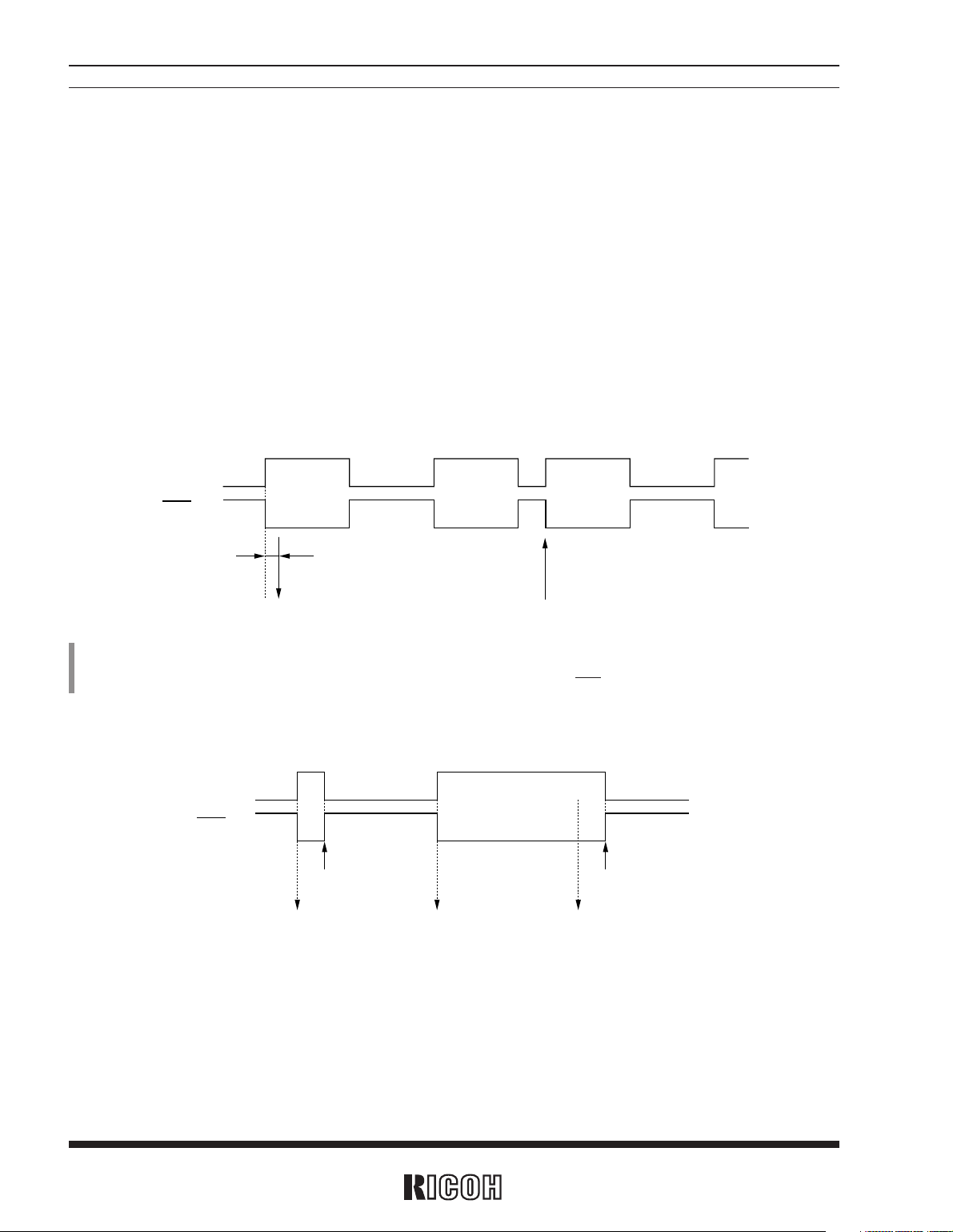
Relation Between the Mode Waveform and the CTFG Bit
• Pulse mode
Approx. 92µs
CTFG bit
INTR pin
(Increment of second counter)
Rewriting of the second counter
• Level mode
Setting CTFG bit to 0
(Increment of
second counter)
Setting CTFG bit to 0
CTFG bit
INTR pin
(Increment of
second counter)
(Increment of
second counter)
*
) In the pulse mode, the increment of the second counter is delayed by approximately 92µs from the falling edge of clock pulses. Consequently, time
readings immediately after the falling edge of clock pulses may appear to lag behind the time counts of the real-time clocks by approximately 1 second.
Rewriting the second counter will reset the other time counters of less than 1 second, driving the INTR pin low.
2) Level Mode : periodic interrupt signals are output with selectable interrupt cycle settings of 1 second, 1 minute, 1
hour, and 1 month. The increment of the second counter is synchronized with the falling edge of
periodic interrupt signals. For example, periodic interrupt signals with an interrupt cycle setting of
1 second are output in synchronization with the increment of the second counter as illustrated in
the timing chart below.
3) When the oscillation adjustment circuit is used, the interrupt cycle will fluctuate once per 20 seconds as follows:
Pulse Mode : the “L” period of output pulses will increment or decrement by a maximum of ±3.784ms.
For example, 1-Hz clock pulses will have a duty cycle of 50 ±0.3784%.
Level Mode : a periodic interrupt cycle of 1 second will increment or decrement by a maximum of ±3.784ms.
13
R×5C338A
VDSL Description
0 Selecting the supply voltage monitoring threshold setting of 2.1 volts.
1 Selecting the supply voltage monitoring threshold setting of 1.6 volts.
2.2-1 VDSL
Supply Voltage Monitoring Threshold Selection Bit
The VDSL bit is intended to select the supply voltage monitoring threshold settings.
VDET Description
0
Indicating supply voltage above the supply voltage monitoring threshold settings.
1
Indicating supply voltage below the supply voltage monitoring threshold settings.
2.2-2 VDET
Supply Voltage Monitoring Result Indication Bit
(Default setting)
Once the VDET bit is set to 1, the supply voltage monitoring circuit will be disabled while the VDET bit will hold the
setting of 1. The VDET bit accepts only the writing of 0, which restarts the supply voltage monitoring circuit.
Conversely, setting the VDET bit to 1 causes no event.
D7 D6 D5 D4 D3 D2 D1 D0
VDSL VDET
SCRATCH
XSTP CLEN1 CTFG WAFG DAFG
VDSL VDET
SCRATCH
XSTP CLEN1 CTFG WAFG DAFG
0 0 0 1 0 0 0 0
2.2 Control Register 2 (at Address Fh)
(For writing)
(For reading)
Default setting*
SCRATCH Description
0
1
2.2-3 SCRATCH
Scratch Bit
(Default setting)
The SCRATCH bit is intended for scratching and accepts the reading and writing of 0 and 1. The SCRATCH bit will
be set to 0 when the XSTP bit is set to 1 in the control register 2.
(Default setting)
*
) Default settings: Default value means read/written values when the XSTP bit is set to “1” due to power-on from 0 volts or supply voltage drop.
 Loading...