Dec. 15 ’97
I2C-bus Serial Interface
Real Time Clock (8pin SSOP)
RS5C372B
■ OUTLINE
The RS5C372B is a CMOS type real-time c lock which is connected to the CPU via 2-wire and c apable of s erial
transmission of clock and calendar data to the CPU. The RS5C372B can generate various periodic interrupt
clock pulses lasting for long period (one m onth), and alarm interrupt can be m ade by days of the week, hours,
and minutes by two incorporated systems. Since an oscillation circuit is driven at a constant voltage, it
undergoes fluctuations of few voltage and consequently offers low current consum ption (0.5µ A at 3V). It also
provides an oscillator halt sensing function applicable for data validation at power-on and other occas ions and
32kHz clock output (CMOS output) for an external micro computer. The product also incorporates a time
trimming circuit that adjusts the clock with higher precision by adjusting any errors in crystal oscillator
frequencies based on signals from the CPU. The crystal oscillator may be selected between 32.768kHz or
32.000kHz types. Integrated into an ultra com pact and ultra thin 8 pin SSO P package, the RS5C372B is the
optimum choice for equipment requiring small sized and low power consuming products.
■ Features
● Time keeping voltage 1.45V to 6.0V
● Lowest supply current 0.5µA TYP (0.9µA MAX)
(0.9µA MAX) at 3V(-40 to +85°C)
● Connected to the CPU via only 2-wire (I
2
C-bus interface, max.400KHz, address 7bits)
● A clock counter (hours, minutes, and seconds) and a calendar counter (leap years, years, months, days,
and days of the week) in BCD codes
● Interrupt to the CPU (period of one month to half second, with interrupt flag, interrupt halt function)
(/INTR)
● Two systems of alarm functions (days of the week, hours, and minutes) (/INTR)
● Oscillation halt sensing to judge internal data validity
● Clock output of 32.768kHz(32.000kHz) ( output controllable via a register)
(32KOUT:CMOS push-pull output)
● Second digit adjustment by ±30 seconds
● Automatic leap year recognition up to the year 2099
● 12-hour or 24-hour time display selectable
● Oscillation stabilizing capacity (CG, CD) incorporated
● High precision clock error adjustment circuit
● Oscillator of 32.768kHz or 32.000kHz may be used
● CMOS logic
● Package:8pin SSOP
2
*) I
C-bus is a trademark of PHILIPS ELECTRONICS N.V.
at 3V(25°C)
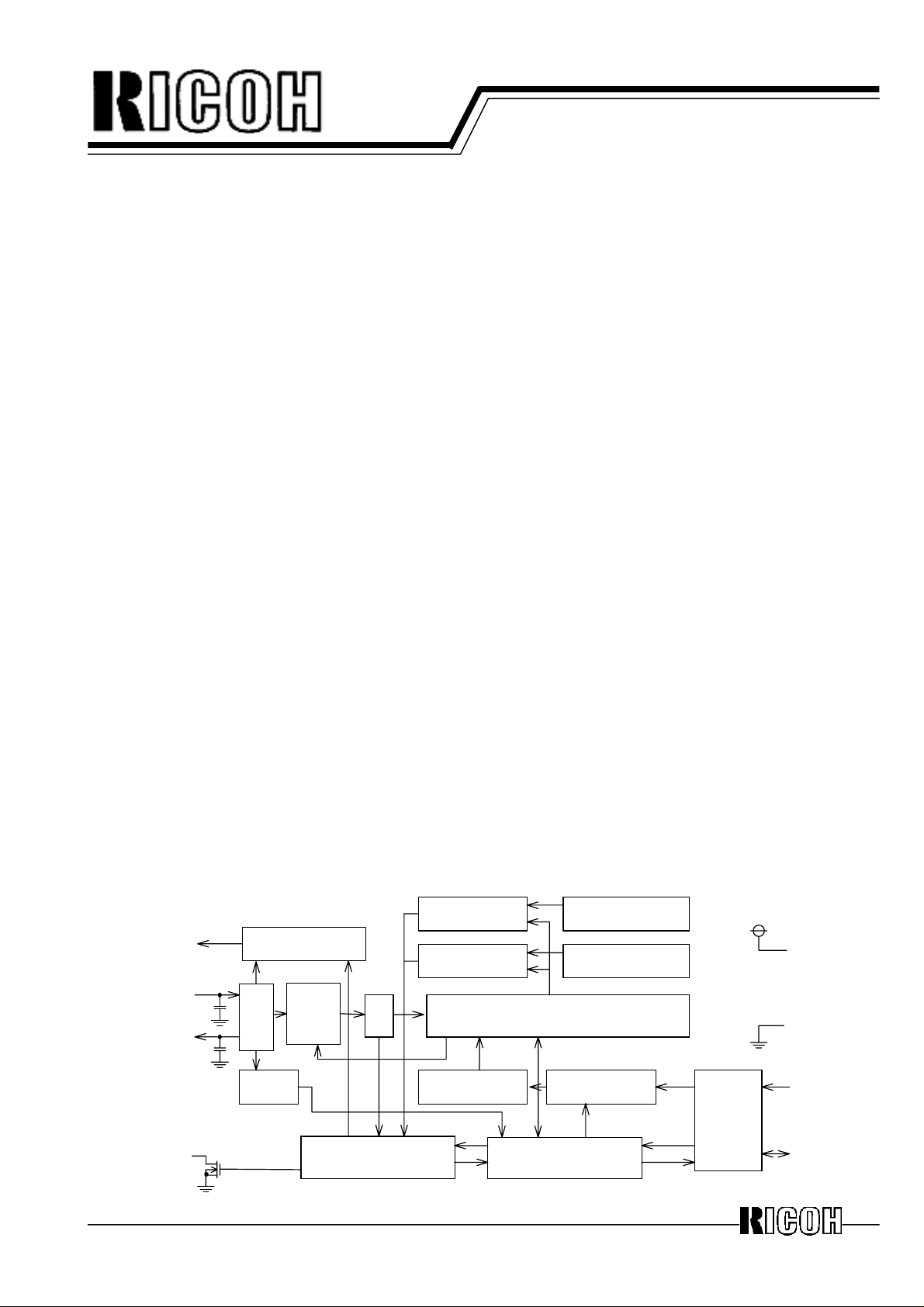
■ Block Diagram
32KOUT
OSCIN
OSCOUT
/INTR
32kHz OUTPUT
CONTROL
DIVIDER
CORREC
OSC
OSC
DETECT
-TION
DIV
INTERRUPT CONTROL
COMPARATOR_A
COMPARATOR_B
TIME COUNTER
(SEC,MIN,HOUR,WEEK,DAY,MONTH,YEAR)
ADDRESS
DECODER
SHIFT REGISTER
ALARM_A REGISTER
(WEEK,MIN,HOUR)
ALARM_B REGISTER
(WEEK,MIN,HOUR)
ADDRESS
REGISTER
- 1 -
VDD
VSS
SCL
I/O
CONTROL
SDA
RS5C372B
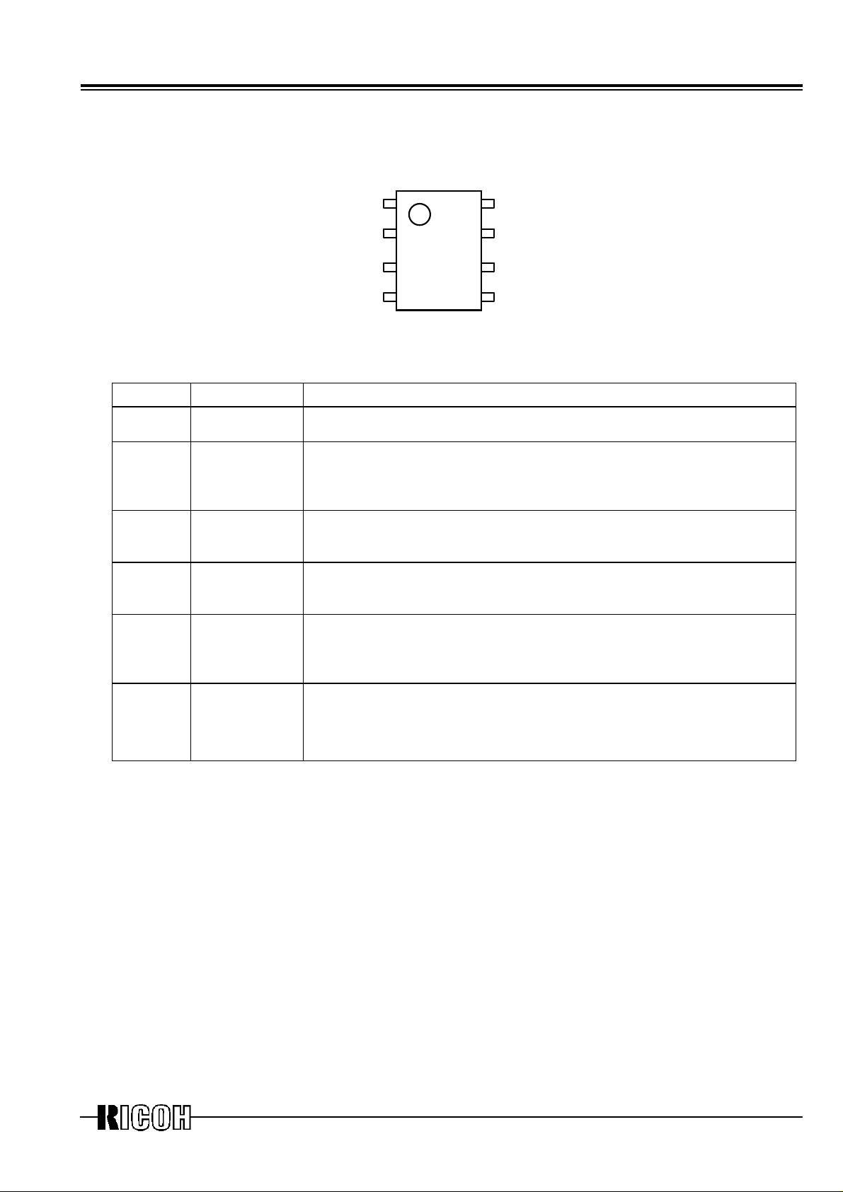
■ Pin Configuration
RS5C372B (8PIN SSOP)
32KOUT
SCL
SDA
VSS
1
2
3
45
8
7
6
VDD
OSCIN
OSCOUT
/INTR
TOP VIEW
■ Pin Description
Symbol Pin Name Description
SCL Shift clock input This pin is used to input shift clock pulses to synchronize data input/output to
and from the SDA pin with this clock. Up to 6V beyond VDD may be input.
SDA Serial input
output
This pin inputs and outputs written or read data in synchronization with shift
clock pulses from the SCL pin. Up to 6V beyond VDD may be input. This
pin functions as an Nch open drain output.
/INTR Interrupt
output
This pin outputs periodic interrupt pulses and alarm interrupt (ALARM_A,
ALARM_B) to the CPU. This pin is off when power is activated from 0V.
This pin functions as an Nch open drain output.
32KOUT 32K Clock
Output
This pin outputs 32.768kHz pulses (when 32.768kHz crystal is used),
It outputs 32.768kHz when power source is activated from 0V. This pin
functions as an CMOS push-pull output.
OSCIN
OSCOUT
Oscillator
circuit
input/output
These pins configure an oscillator circuit by connecting a 32.768kHz or
32.000kHz crystal oscillator between the OSCIN–OSCOUT pins.
(Any other oscillator circuit components are built into the RS5C372B.)
VDD
VSS
Positive power
supply input
Negative power
supply input
The VDD pin is connected to the positive power supply and Vss to the
ground.
- 2 -
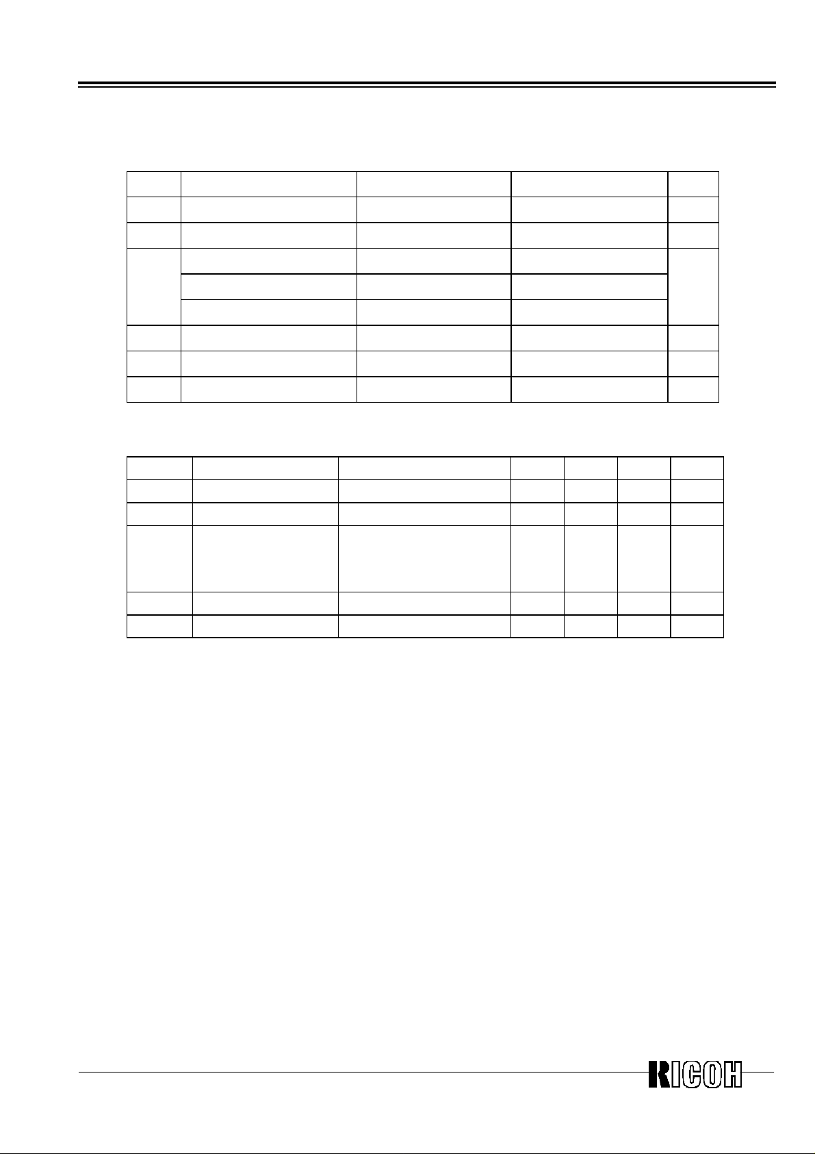
■ Absolute Maximum Ratings
Symbol Item Conditions Ratings Unit
VDD Supply Voltage -0.3 to +7.0 V
VI Input Voltage SCL, SDA -0.3 to +7.0 V
VO Output Voltage 1 SDA -0.3 to +7.0 V
Output Voltage 2 /INTR -0.3 to +12.0
Output Voltage 3 32KOUT -0.3 to VDD+0.3
PD Power Dissipation Topt=25°C 300 mW
Topt Operating Temperature -40 to +85 °C
Tstg Storage Temperature -55 to +125 °C
■ Recommended Operating Conditions
Symbol Item Conditions MIN. TYP. MAX. Unit
VDD Operating Voltage 2.0 6.0 V
VCLK Time Keeping Voltage 1.45 6.0 V
FXT Oscillation Frequency 32.768
VPUP1 Pull up Voltage 1 SCL, SDA 6.0 V
VPUP2 Pull up Voltage 2 /INTR 10.0 V
RS5C372B
(VSS=0V)
(VSS=0V, Topt=-40 to +85°C)
kHz
or
32.000
- 3 -
RS5C372B
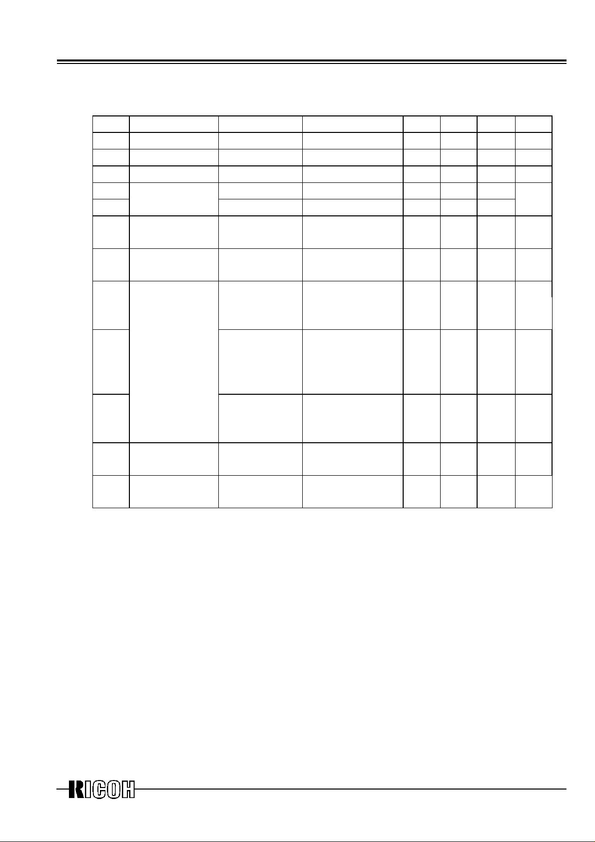
■ DC Characteristics
Unless otherwise specified: VSS=0V, VDD=3V, Topt=-40 to +85°C, Oscillation Frequency=32.768kHz or 32.000KHz(R1=30kΩ)
Symbol Item Pin Name Conditions MIN. TYP. MAX. Unit
VIH “H” input Voltage SCL, SDA 0.8
VIL “L” input voltage SCL, SDA -0.3 0.2
IOH “H” output current 32KOUT VOH=VDD-0.5V -0.5 mA
IOL1 “L” output current /INTR, 32KOUT VOL1=0.4V 1 mA
IOL2 SDA VOL2=0.6V 6
IILK Input leakage
current
IOZ Output off state
leakage current
IDD1 Standby current VDD VDD=3V, Topt=25°C0.50.9µA
IDD2 VDD VDD=3V,
IDD3 VDD VDD=6V 0.8 2.0 µA
SCL,SDA=6V
CG Internal oscillation
capacitance 1
CD Internal oscillation
capacitance 2
SCL VI=6V or VSS
VDD
-1 1 µA
6.0 V
VDD
V
VDD=6V
SDA, /INTR,
32KOUT
VO=6V or VSS
VDD=6V
-1 1 µA
SCL,SDA=3V
Output=OPEN *)
1.0 µA
Topt=-40 to +85°C
SCL,SDA=3V
Output=OPEN *)
Output=OPEN *)
OSCIN 10 pF
OSCOUT 10 pF
*) The mode outputs no clock pulses and output is open (output off state).
For consumption current (output: no load) when 32kHz pulses are output from 32KOUT, see "Typical
Characteristics Measurement ".
- 4 -
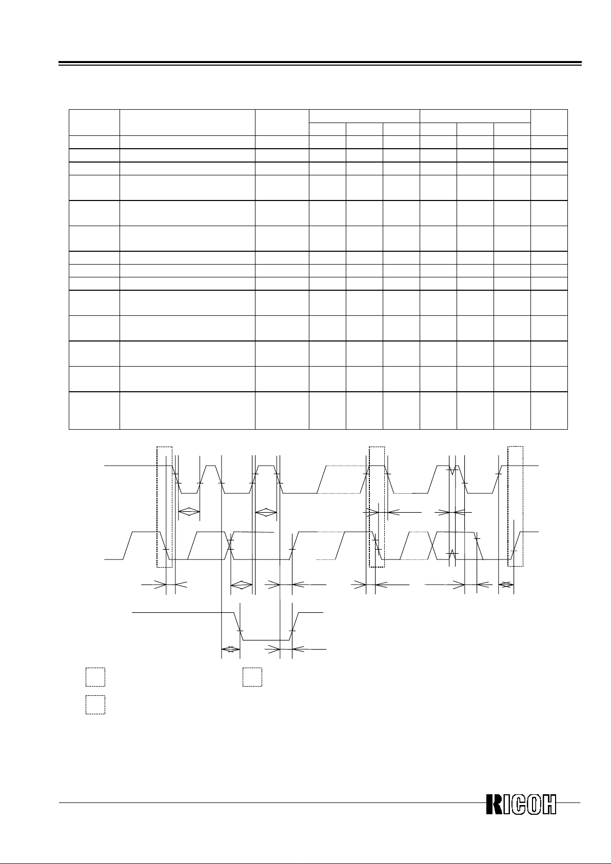
■ AC Characteristics
Unless otherwise specified: VSS=0V,Topt=-40 to +85°C
I/O Conditions: VIH=0.8×VDD,VIL=0.2×VDD,VOL=0.2×VDD,CL=50pF
Symbol Item
f
SCL
t
LOW
t
HIGH
t
HD;STA
SCL clock frequency 0 100 0 400 kHz
SCL clock “L” time 4.7 1.3
SCL clock “H” time 4.0 0.6
Hold time for a (repeated)
start condition
t
SU;STO
Set-up time for a stop
condition
t
SU;STA
Set-up time for a repeated
start condition
t
SU;DAT
t
HDH;DAT
t
HDL;DAT
t
PL;DAT
Data set-up time 250 100 ns
“H” Data hold time 0 0 ns
“L” Data hold time 35 35 ns
SDA low stable time after
falling of SCL
t
PZ;DAT
SDA off stable time after
falling of SCL
t
R
Rising time of SCL and
SDA (input)
t
F
Falling time of SCL and
SDA (input)
t
SP
Pulse width of spikes whic h
must be suppres sed by the
input Filter
Condi-
tions
RS5C372B
VDD≥2.0V VDD≥2.5V
MIN. TYP. MAX. MIN. TYP. MAX.
4.0 0.6
4.0 0.6
4.7 0.6
2.0 0.9
2.0 0.9
1000 300 ns
300 300 ns
50 50 ns
Unit
µs
µs
µs
µs
µs
µs
µs
SCL
SDA(IN)
SDA(OUT)
S
Sr
S
t
LOW
t
PL;DAT
t
SU;DAT
t
HD;STA
Start Condition
Repeated Start condition
Sr P
t
HIGH
t
HDL;DAT
t
PZ;DAT
Stop Condition
P
*For detailed information refer to ”■Operation 1.2. I2C-BUS
transmission system”
t
HD;STAtSP
t
SU;STA
t
HDH;DAT
t
SU;STO
- 5 -
RS5C372B
0.05
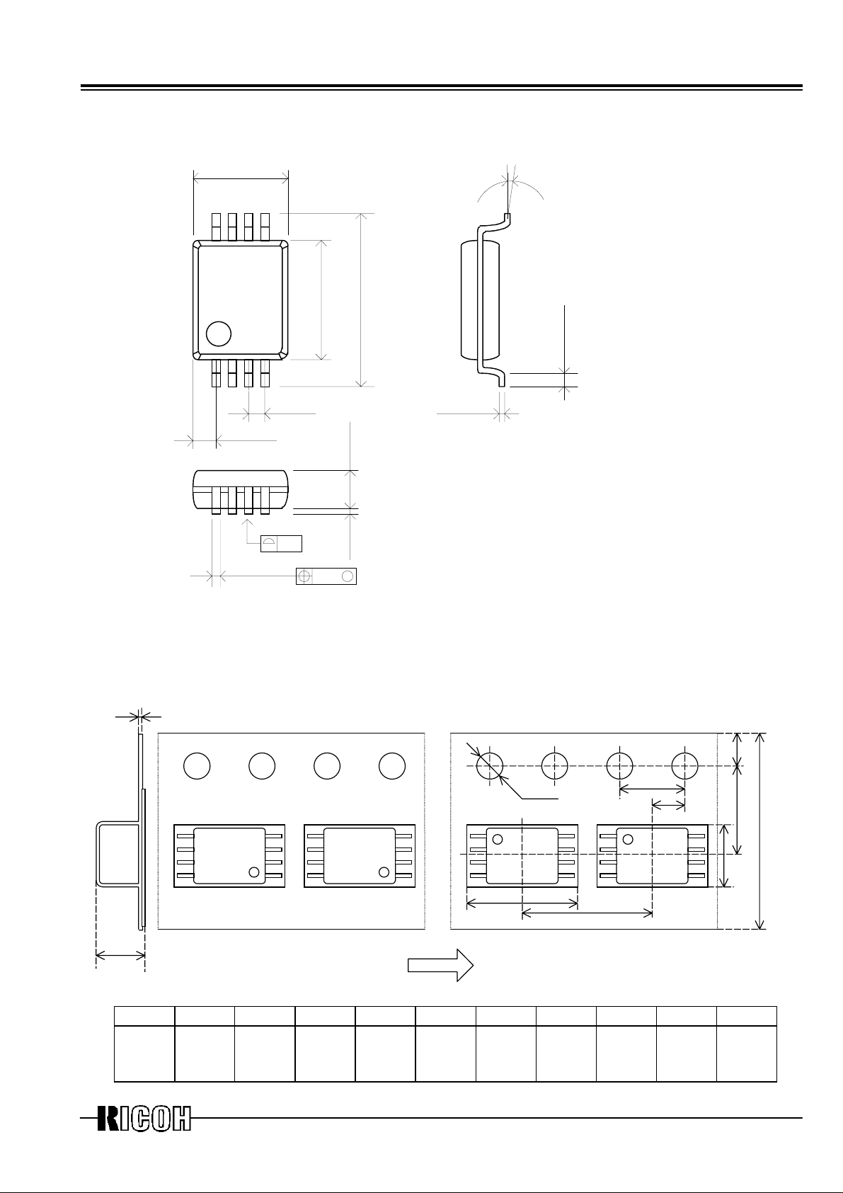
■ Package Dimensions (Unit : mm)
● RS5C372B (8pin SSOP)
3.5±0.3
85
1
0.775TYP.
0.22±0.1
■ Selection Guide
Taping type can be designated as follows: (Standard type is E2)
RS5C372B-E1, RS5C372B-E2
■ Taping Specification
0 to 10
°
0.2
0.3
±
±
4.4
6.4
4
0.65
0.10.1
±
1.15
0.1
0.15
±
M
0.15
0.15
+0.1
-
0.3
±
0.5
T
T
2
A
0
B
6.7 3.9 12.0
E
P
0
P
2
F
W
B
0
E1
D
∅
0
A
0
P
1
E2
User Direction of F ee d
Unit:mm
0
WFEP1P
±0.3
5.5
±0.05
1.75
±0.1
8.0
±0.1
2
2.0
±0.05
P
0
4.0
±0.1
D
0
1.5
+0.1
TT
0.3
±0.1
2
2.7
Max
0
- 6 -

RS5C372B
■■■■ Outline Description
1. Interfacing with the CPU
The RS5C372B reads/writes data over I
Since the output of the I/O pin of SDA is open drain, data interfacing with a CPU with different supply
voltage is possible by applying pull-up resistance on the circuit board. The maximum clock frequency of
400kHz of SCL enables data transfer in I
2. Clock function
The clock func tion of the RS5C372B allows write/read data from lower two digits of the dominical year to
seconds to and from the CPU. When lower two digits of the dominical year are m ultiples of 4, the year is
recognized as a leap year automatically. Up to the year 2099 leap years will be automatically recognized.
*) The year 2000 is a leap year while the year 2100 is not.
3. Alarm function
The RS5C372B has an alarm function that outputs an interrupt s ignal from /INTR output pins to the CPU
when the day of the week, hour or minute corresponds to the setting. These two systems of alarms
(ALARM_A, ALARM_B), each may output interrupt s ignal separ ately at a spec if ied time. The alarm may be
selectable between on and off for each day of the week, thus allowing outputting alarm everyday or on a
specific day of the week.
The ALARM_A and ALARM_B is output from the /INTR pins. Polling is possible separately for each alarm
system.
4. High precision time trimming function
The RS5C372B has internal oscillation c ircuit capacitance CG and CD so that an oscillation circuit may be
configured simply by externally connecting a crystal. Either 32.768kHz or 32.000kHz may be selected as a
crystal oscillator by setting the internal register appropriately. The RS5C372B incorpor ates a tim e trim ming
circuit that adjusts gain or loss of the clock from the CPU up to approx. ±189ppm (±194ppm when 32.000kHz
crystal is used) by approximately 3ppm steps to cor rect discrepancy in oscillation frequency. (Error after
correction:±1.5ppm:25°C)
Thus by adjusting frequencies for each system,
• Clock display is possible at much higher precision than conventional real-time clock while using a
crystal with broader fluctuation in precision.
• Even seasonal frequency fluctuation may be corrected by adjusting seasonal clock error.
• For those systems that have temperature detection precision of clock function may be increased by
correcting clock error according to temperature fluctuations.
5. Oscillation halt sensing
The oscillation halt sensing function uses a register to store oscillation halt infor mation. This function may
be used to determine if the RS5C372B supply power has been booted from 0V and if it has been backed up.
This function is useful for deter-mining if clock data is valid or invalid.
6. Periodic interrupt
The RS5C372B can output periodic interrupt pulses in addition to alarm function from the /INTR pin. This
frequency may be selected from 2Hz (every 0.5 seconds), 1Hz (every second), 1/60Hz (every minute),
1/3600Hz (every hour) and monthly (1st of month).
Output wave form for periodic interrupt may be selected from regular pulse wave form (2Hz and 1Hz) and
wave forms (every second, every minute, every hour and every month) that are appropriate for CPU level
interrupt. The RS5C372B has polling function that monitors pin status in the register.
7. 32kHz clock output
The RS5C372B may output oscillation frequency from the 32KOUT pin. This clock output is set for output by
default, which is set to on or off by setting the register. This pin functions as an CMOS push-pull output.
2
C-bus interface via two signal lines: SDA (data) and SCL (clock).
2
C-bus high-speed mode.
- 7 -

RS5C372B
Notes:
The year-digit counter of RS5C372B counts only lower two digits of a year and no counter is supplied f or
upper two digits. When you are going to use this product in a system that must cope with “2000 year
problem” which shall be corrected by software.
Notes:
Purchase of I
2
C components of Ricoh Company, Ltd. conveys a license under the Philips I2C Patent Rights to
use these components in an I
Specification as defined by Philips.
2
C system, provided that the system comforms to the I2C Standard
- 8 -
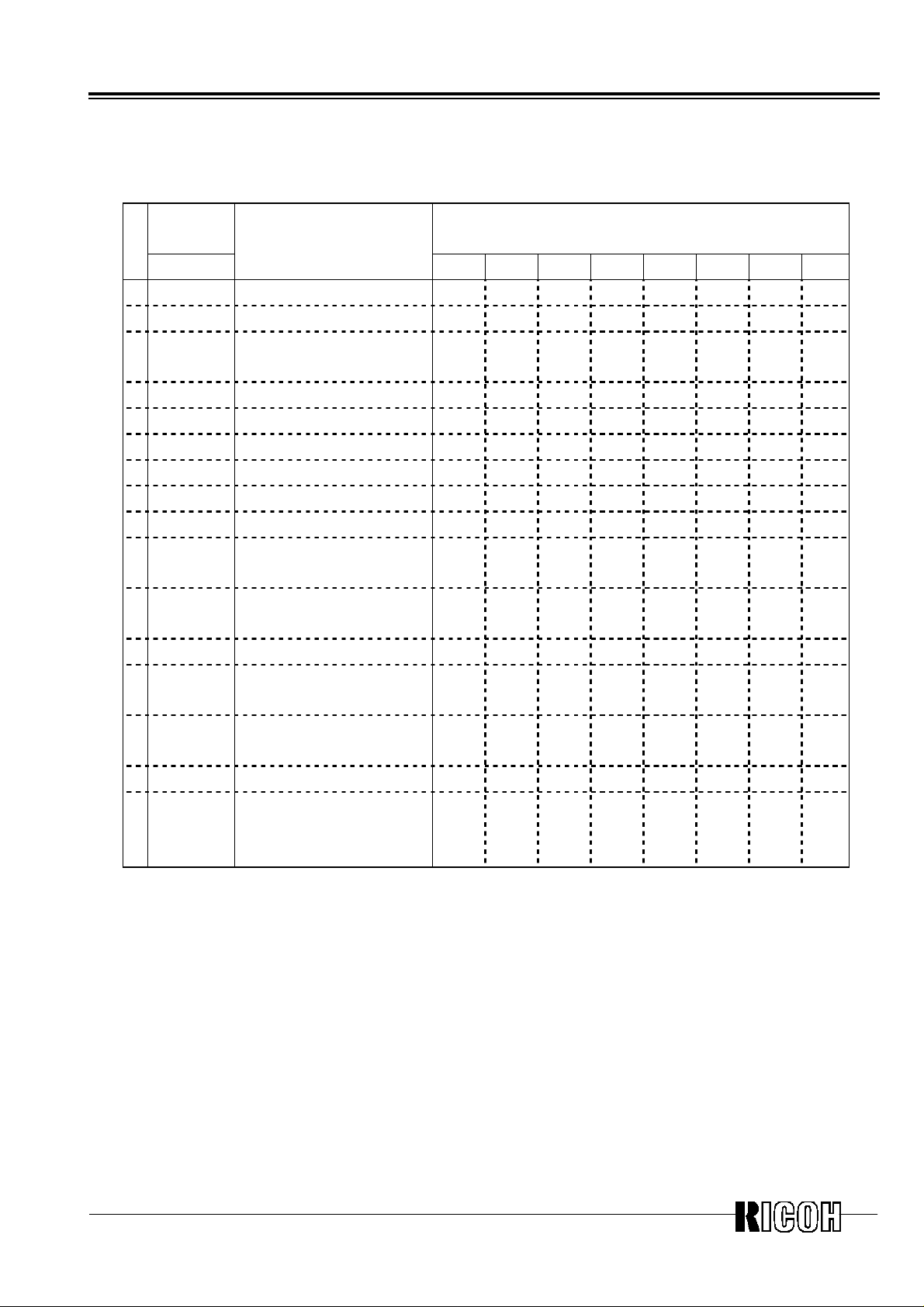
■ Functional Description
1. Allocation of Internal Addresses
RS5C372B
Internal
Address
A3A2A1A0 D7 D6 D5 D4 D3 D2 D1 D0
0 0 0 0 0 Second Counter -*2) S40 S20 S10 S8 S4 S2 S1
1 0 0 0 1 Minute Counter - M40 M20 M10 M8 M4 M2 M1
2 0 0 1 0 Hour Counter - - H20 H10 H8 H4 H2 H1
3 0 0 1 1 Day-of- the-Week Counter - - - - - W4 W2 W1
4 0 1 0 0 Day Counter - - D20 D10 D8 D4 D2 D1
5 0 1 0 1 Month Counter - - - MO10 MO8 MO4 MO2 MO1
6 0 1 1 0 Year Counter Y80 Y40 Y20 Y10 Y8 Y4 Y2 Y1
7 0 1 1 1 Time Trimming Register /XSL F6 F5 F4 F3 F2 F1 F0
8 1 0 0 0 Alarm_A (Minute Register) - AM40 AM20 AM10 AM8 AM4 AM2 AM1
9 1 0 0 1 Alarm_A (Hour Register) - - AH20 AH10 AH8 AH4 AH2 AH1
A 1 0 1 0 Alarm_A
B 1 0 1 1 Alarm_B (Minute Register) - BM40 BM20 BM10 BM8 BM4 BM2 BM1
C 1 1 0 0 Alarm_B (Hour Register) - - BH20 BH10 BH8 BH4 BH2 BH1
D 1 1 0 1 Alarm_B
E 1 1 1 0 Control Register 1 AALE BALE 0 *5) 0 *5) TEST CT2 CT1 CT0
F 1 1 1 1 Control Register 2 - - /12⋅24 ADJ
Contents Data *1)
P⋅/A
AP⋅/A
- AW6 AW5 AW4 AW3 AW2 AW1 AW0
-of-
(Day
(Day
the-week Register)
-of-
the-week Register)
BP⋅/A
- BW6 BW5 BW4 BW3 BW2 BW1 BW0
XSTP
*3),*4)
/CLEN CTFG AAFG BAFG
*1) All the listed data can be read and written except for ADJ/XSTP.
*2) The “–” mark indicates data which can be read only and set to “0” when read.
*3) The ADJ/XSTP bit of the control register2 is set to ADJ for write and XSTP for read operation.
The XSTP bit is set to “0” by writing data into the control register2 for normal oscillation.
*4) When XSTP is set to “1” the /XSL, F6 to F0, CT2 to CT0, AALE, BALE, /CLEN and TEST bits
are reset to “0”.
*5) These bits must be set to “0” in any case.
- 9 -
RS5C372B
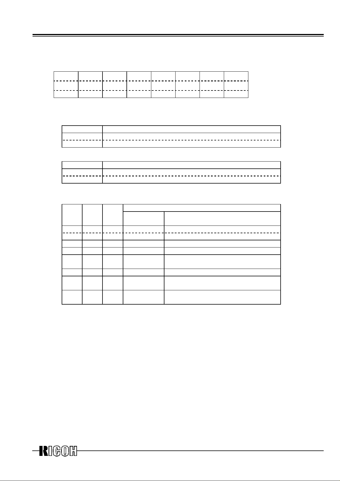
2. Functions of Registers
2.1. Control Register 1 (Internal address at Eh)
D7 D6 D5 D4 D3 D2 D1 D0
AALE BALE 0 *1) 0 *1) TEST CT2 CT1 CT0
AALE BALE 0 0 TEST CT2 CT1 CT0
00000000Default *2)
*1) These bits must be set “0” in any case.
*2) The default means read values when XSTP=”1” by after initial power-on or supply voltage drop,etc.
2.1.1. AALE,BALE Alarm_A, Alarm_B enable bit
AALE,BALE Description
0 Alarm_A (Alarm_B) correspondence action invalid (Default)
1 Alarm_A (Alarm_B) correspondence action valid
2.1.2. TEST Test bit
TEST Description
0 Ordinary operation mode (Default)
1 Test mode
The test bit is used for IC test. Set the TEST bit to 0 in ordinary operation
(For write operation)
(For read operation)
.
2.1.3. CT2,CT1,CT0 Periodic interrupt frequency select bit
CT2 CT1 CT0
Wave form
Description
Frequency and falling timing
mode
0 0 0 - OFF(H) (Default)
0 0 1 - Fixed at “L”
0 1 0 Pulse mode 2Hz(Duty50%)
0 1 1 Pulse mode 1Hz(Duty50%)
1 0 0 Level mode Every second (synchronized with second
count up)
1 0 1 Level mode Every minute (00 second of every minute)
1 1 0 Level mode Every hour ( 00 minute(s) 00 second(s) of
every hour )
1 1 1 Level mode Every month (the 1st day 00 AM 00
minute(s) 00 second(s) of every month )
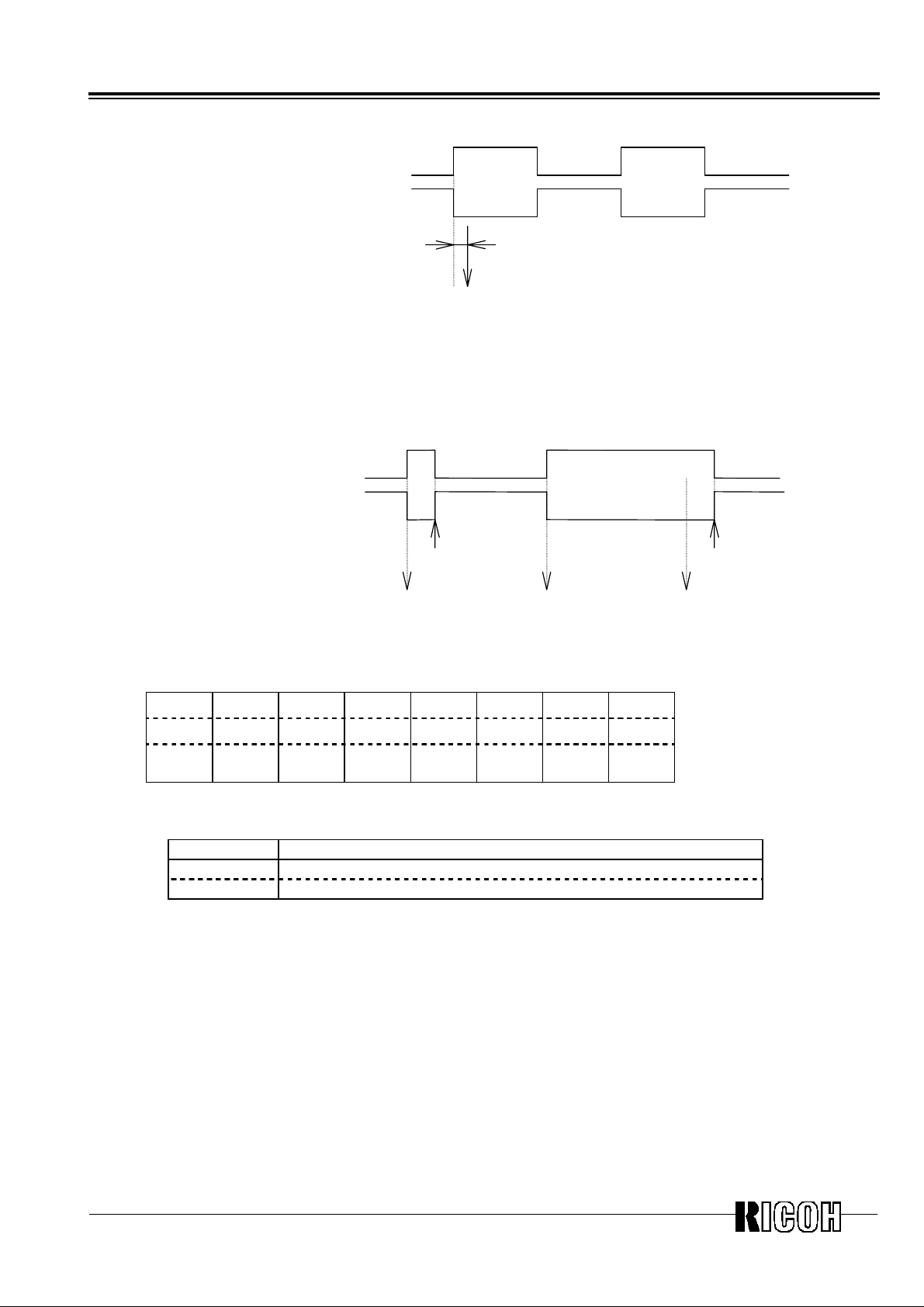
1) Pulse mode: Outputs 2Hz, 1Hz clock pulses. For relationships with counting up of seconds, see the diagram
on the next page.
*) When 32000Hz crystal is used
In the 2Hz clock pulse mode, 0.496s clock pulses and 0.504s clock pulse are output alternately. Duty cycle for
1Hz clock pulses becomes 50.4% (“L” duration is 0.496s while “H” duration is 0.504s).
2) Level mode: One second, one minute or one month may be selected for an interrupt frequency. Counting up of
seconds is matched with falling edge of interrupt output.
3) When the clock error correction circuit is used, periodic interrupt frequency changes every 20 seconds.
Pulse mode: “L” duration of output pulses may change in the maximum range of ±3.784ms (±3.875ms when
32.000kHz crystal is used.) For example, Duty will be 50±0.3784% (or 50±0.3875% when 32.000kHz crystal is
used) at 1Hz.
Level mode: Frequency in one second may change in the maximum range of ±3.784ms (±3.875ms when
32.000kHz crystal is used.)
- 10 -
Pulse mode
Level mode
RS5C372B
CTFG bit
/INTR pin
Approx. 92µs (32.768KHz crystal is used)
Approx. 94µs (32.000KHz cristal is used)
(Counting up of seconds)
*) Since counting up of seconds and the fal ling edge has a time lag of approx. 92µs (at
32.768kHz) (approx. 94µs when 32.000kHz crystal is used), time with apparently
approx. one second of delay from time of the real-time clock may be read when time is
read in synchronization with the falling edge of output.
CTFG bit
/INTR pin
Write 0 to CTFG bit
(second count-up)
2.2. Control Register 2 ( Internal address at Fh )
D7 D6 D5 D4 D3 D2 D1 D0
--/12⋅24 ADJ /CLEN CTFG AAFG BAFG
00/12⋅24 XSTP /CLEN CTFG AAFG BAFG
0 0 unde-
10000Default (*)
fined
*)The default means read values when XSTP=”1” by after initial power-on or supply voltage drop,etc.
2.2.1. /12⋅24 /12⋅24-hour Time Display Selection bit
/12⋅24
Description
0 12-hour time display system
1 24-hour time display system
Being set this bit at “0” indicates 12-hour display system while “1” indicates 24-hour system.
Write 0 to CTFG bit
(second count-up)(second count-up)
(For Write operation )
(For Read operation )
- 11 -
RS5C372B
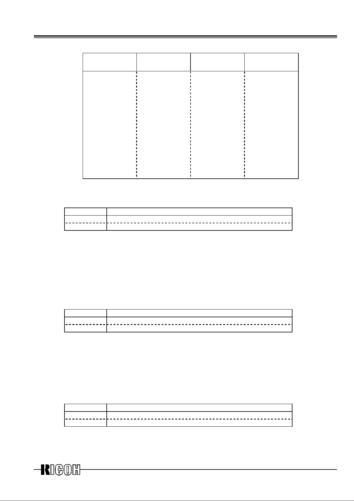
*) Either the 12-hour or 24-hour time display system should be selected before writing time data.
Time Display Digit Table
24-hour time
display system
00 12 (AM12) 12 32 (PM12)
01 01 (AM 1) 13 21 (PM 1)
02 02 (AM 2) 14 22 (PM 2)
03 03 (AM 3) 15 23 (PM 3)
04 04 (AM 4) 16 24 (PM 4)
05 05 (AM 5) 17 25 (PM 5)
06 06 (AM 6) 18 26 (PM 6)
07 07 (AM 7) 19 27 (PM 7)
08 08 (AM 8) 20 28 (PM 8)
09 09 (AM 9) 21 29 (PM 9)
10 10 (AM10) 22 30 (PM10)
11 11 (AM11) 23 31 (PM11)
12-hour time
display system
24-hour time
display system
12-hour time
display system
2.2.2. ADJ ±30 Second Adjust Bit
ADJ Description
0 Ordinary operation
1 Second digit adjustment
• The following operations are performed by setting the second ADJ bit to 1.
1) For second digits ranging from “00” to “29” seconds:
Time counters smaller than seconds are reset and second digits are set to “00”.
2) For second digits ranging from “30” to “59” seconds:
Time counters smaller than seconds are reset and second digits are set to “00”. Minute digits
are incremented by 1.
• Second digits are adjusted within 122µs (within 125µs:when 32.000kHz crystal is used) from writing
operation to ADJ.
• The ADJ bit is for write only and allows no read operation.
2.2.3. XSTP Oscillator Halt Sensing Bit
XSTP Description
0 Ordinary oscillation
1 Oscillator halt sensing (Default)
The XSTP bit senses the oscillator halt.
• When oscillation is halted after initial power on from 0V or drop in supply voltage the bit is set to “1”
and which remains to be “1” after it is restarted. This bit may be used to judge validity of clock and
calendar count data after power on or supply voltage drop.
• When this bit is set to “1”, /XSL, F6-F0, CT2, CT1, CT0, AALE, BALE, /CLEN and TEST bits are
reset to “0”. /INTR will stop output and the 32KOUT outputs 32kHz clock pulses.
• The XSTP bit is set to "0" by setting some data to the control register 2 (address Fh) during ordinary
oscillation.
2.2.4. /CLEN 32kHz Clock Output Bit
/CLEN Description
0 32kHz clock output enabled (Default)
1 32kHz clock output disabled
By setting this bit to “0”, output of clock pulses of the same frequency as the crystal oscillator from
32KOUT pin, is enabled.
- 12 -
 Loading...