RICOH RS5C372A, RS5C372B Technical data

RS5C372A/B
I2C bus SERIAL INTERFACE REAL-TIME CLOCK IC
NO.EA-044-100928
OUTLINE
The RS5C372A is a CMOS type real-time clock which is connected to the CPU via 2-wires and capable of
serial transmission of clock and calendar data to the CPU.
The RS5C372A can generate various periodic interrupt clock pulses lasting for long period (one month), and
alarm interrupt can be made by days of the week, hours, and minutes by two incorporated systems. Since an
oscillation circuit is driven at a constant voltage, it undergoes fluctuations of few voltage and conseq uent ly offers
low current consumption (T yp. 0.5μA at 3V). It also provides an oscillator h alt sensing function appli cable for data
validation at power-on and other occasions and 32-kHz clock output for an external micro computer. (Nch. open
drain output) The product also incorporates a time trimming circuit that adjusts the clock with higher precision
by adjusting any errors in crystal oscillator frequencies based on signals from the CPU. The crystal oscillator
may be selected from 32.768kHz or 32.000kHz types. Integrated into an ultra comp act and ultra thin 8 pin SSOP
package, the RS5C372A is the optimum choice for equipment requiring small sized and low power consuming
products.
FEATURES
• Time keeping voltage: 1.3V to 6.0V
• Lowest supply current: 0.5μA Typ. (0.9μA Max.) : 3V (25°C)
(1.0μA Max.) : 3V (−40 to +85°C)
• Connected to the CPU via only 2−wires (I
• A clock counter (counting hours, minutes, and se conds) and a cal endar counter (co unting leap years, years,
months, and days of the week) in BCD codes
• Interrupt to the CPU (period of one month to one second, interrupt flag, interrupt halt
function)(
• Two systems of alarm functions (days of the week, hours, and minutes) (
• Oscillation halt sensing to judge internal data validity
• Clock output of 32.768kHz (32.000kHz) (output controllable via a register) ⋅⋅⋅ (Nch. open drain output)
• Second digit adjustment by ±30 seconds
• Automatic leap year recognition up to the year 2099
• 12-hour or 24-hour time display selectable
• Oscillation stabilizing capacity (C
• High precision time trimming circuit
• Oscillator of 32.768kHz or 32.000kHz may be used
• CMOS logic
• Package: 8pin SSOP
INTRA
INTRB
,
)
G, CD) incorporated
2
C bus Interface, Max.400kHz, address 7bit)
INTRA
INTRB
,
)
1
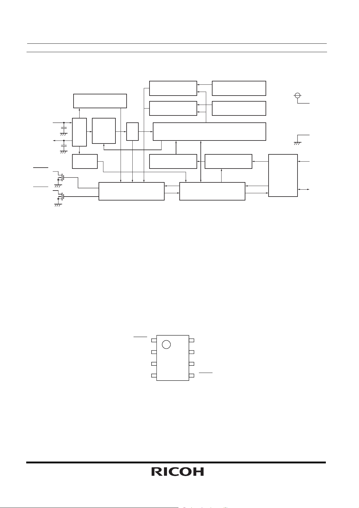
RS5C372A
A
BLOCK DIAGRAM
32kHz OUTPUT
CONTROL
COMPARATOR_A
COMPARATOR_B
ALARM_A REGISTER
(WEEK,MIN,HOUR)
ALARM_B REGISTER
(WEEK,MIN,HOUR)
V
DD
OSCIN
OSC
OSCOUT
DETECT
INTRA
INTRB
OSC
DIVIDER
CORREC
-TION
INTERRUPT CONTROL
DIV
(SEC,MIN,HOUR,WEEK,DAY,MONTH,YEAR)
ADDRESS
DECODER
TIME COUNTER
ADDRESS
REGISTER
SHIFT REGISTER
I/O
CONTROL
APPLICATIONS
• Communication devices (multi function phone, portable phone, PHS or pager)
• OA devices (f ax, portable fax)
• Computer (desk-top and mobile PC, portable word-proce ssor, PDA, electric note or video game)
• AV components (portable audio unit, video camera,camera, digital camera or remote controller)
• Home appliances (rice cooker, electric oven)
• Other(car navigation system,multi-function watch)
V
SS
SCL
SD
PIN CONFIGURATION
2
INTRB
SCL
SDA
V
SS
• 8pin SSOP
1
2
3
4
8
7
6
5
V
DD
OSCIN
OSCOUT
INTRA
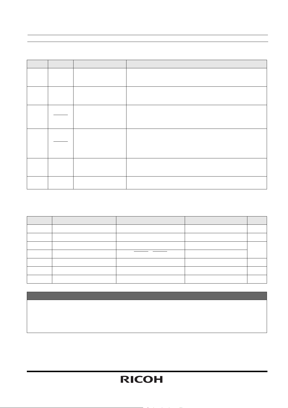
PIN DESCRIPTIONS
Pin No.
2 SCL
Symbol Name Description
Serial Clock Line
3 SDA
Serial Data Line
5
1
7
6
INTRA
INTRB
OSCIN
OSCOUT
Interrupt Output A
Interrupt Output B
Oscillator Circuit
Input/Output
8
4
VDD
V
SS
Positive Power Supply Input
Negative Power Supply Input
RS5C372A
This pin is used to input shift clock pulses to synchronize data
input/output to and from the SDA pin with this clock. Up to 6V
beyond VDD may be input.
This pin inputs and outputs written or read data in synchronization
with shift clock pulses from the SCL pin. Up to 6V beyond V
DD may
be input. This pin functions as an Nch open drain output.
This pin outputs periodic interrupt pulses and alarm interrupt
(Alarm_A, Alarm_B) to the CPU. This pin is off when power is
activated from 0V. This pin functions as an Nch open drain
output.
This pin outputs 32.768kHz clock pulses (when 32.768kHz
crystal is used), periodic interrupt pulses to the CPU or alarm
interrupt (Alarm_B). It outputs 32.768kHz when power source
is activated from 0V. This pin functions as an Nch open drain
output.
These pins configure an osc illator circuit by conn ecting a 32.768k Hz or
32.000kHz crystal oscillator between the OSCIN-OSCOUT pins.
(Any other oscillator circuit components are built into the RS5C372A.)
The VDD pin is connected to the positive power supply and VSS
to the ground.
ABSOLUTE MAXIMUM RATINGS
(Vss=0V)
Symbol Item Conditions Ratinge Unit
VDD Supply Voltage
VI Input Voltag SCL, SDA
VO1 Output Voltage 1 SDA
VO2 Output Voltage 2
PD Power Dissipation
INTRA
Topt=25°C
Topt Operating Temperature
Tstg Storage Temperature
INTRB
,
−0.3 to +7.0
−0.3 to +7.0
−0.3 to +7.0
−0.3 to +12
300 mW
−40 to +85 °C
−55 to +125 °C
ABSOLUTE MAXIMUM RATINGS
Absolute Maximum ratings are threshold limit values that must not be exceeded even for an instant under
any conditions. Moreover, such values for any two items must not be reached simultaneously. Operation
above these absolute maximum ratings may cause degradation or permanent damage to the device.
These are stress ratings only and do not necessarily imply functional operation below these limits.
V
V
V
3
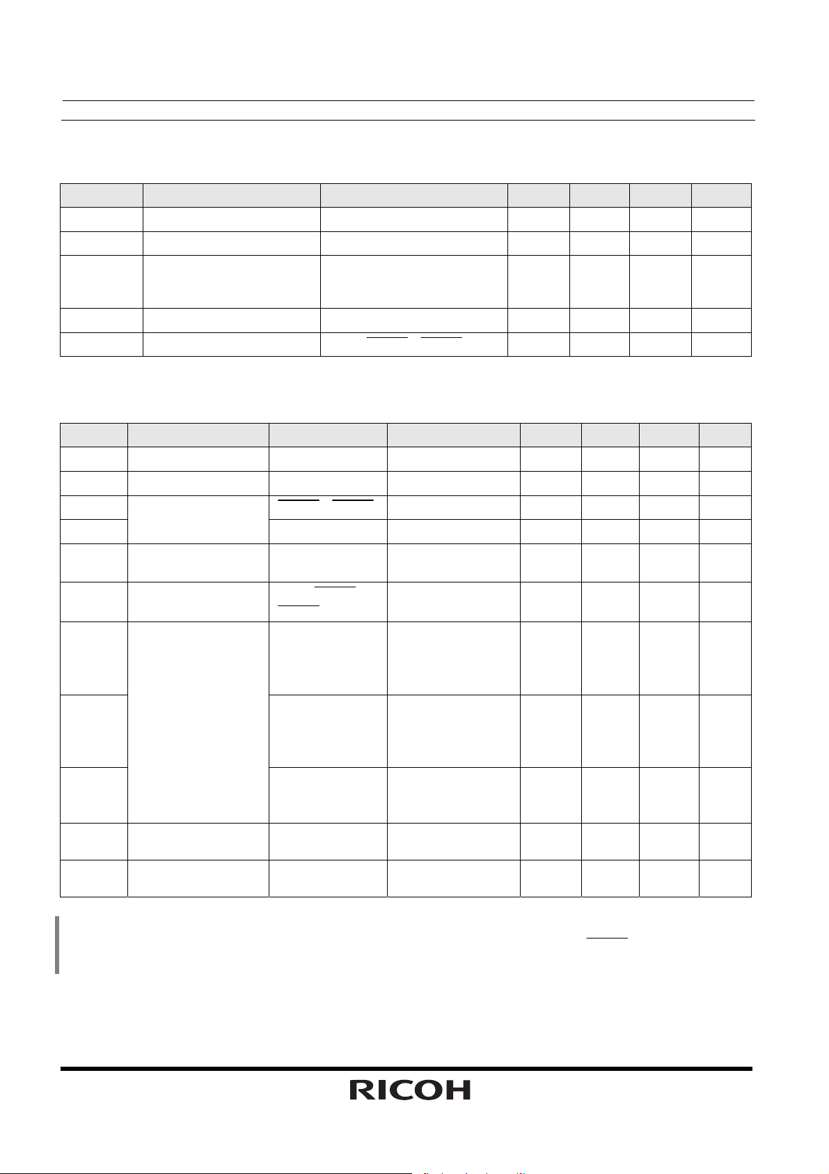
RS5C372A
RECOMMENDED OPERATING CONDITIONS
(Vss=0V,Topt=−40 to +85°C)
Symbol Item Conditions Min. Typ. Max. Unit
VDD Supply Voltage 1.7 6.0 V
VCLK Timekeeping Voltage 1.3 6.0 V
32.768
FXT Oscillation Frequency
or
32.000
VPUP1 Pull-up Voltage 1 SCL, SDA 6.0 V
kHz
VPUP2 Pull-up Voltage 2
INTRA
INTRB
,
10.0 V
DC CHARACTERISTICS
Unless otherwise specified: Vss=0V, VDD=3V, Topt=−40 to +85°C, Oscillation frequency=32.768kHz, or 32.000kHz(R1=30kΩ)
Symbol Item Pin name Conditions Min. Typ. Max. Unit
VIH “H” Input Voltage SCL, SDA 0.8VDD 6.0 V
VIL “L” Input Voltage SCL, SDA
IOL1
IOL2
IILK
IOZ
Output Current
Input Leakage
Current
Output Off State
Leakage Current
INTRA
SDA
SCL
SDA,
INTRB
INTRB
,
INTRA
,
IDD1 VDD
IDD2 VDD
IDD3
CG
CD
Standby Current
Internal Oscillation
Capacitance 1
Internal Oscillation
Capacitance 2
VDD
OSCIN 10 pF
OSCOUT 10 pF
VOL1=0.4V
V
OL2=0.6V
V
I=6V or Vss
DD=6V
V
V
O=6V or Vss
DD=6V
V
DD=3V
V
Topt=25°C
SCL, SDA=3V
Output=OPEN
DD=3V
V
1
∗
Topt=−40 to +85°C
SCL, SDA=3V
Output=OPEN
DD=6V
V
SCL, SDA=6V
Output=OPEN
1
∗
1
∗
−0.3
1 mA
6 mA
−1
−1
0.5 0.9
1.0
0.8 2.0
∗1) The mode outputs no clock pulses when output is open (output off state).
For consumption current (output: no load) when 32kHz pulses are output from
Typical Characteristic Measurements”
0.2VDD V
1
1
INTRB
, see “USAGES, 6.
μA
μA
μA
μA
μA
4
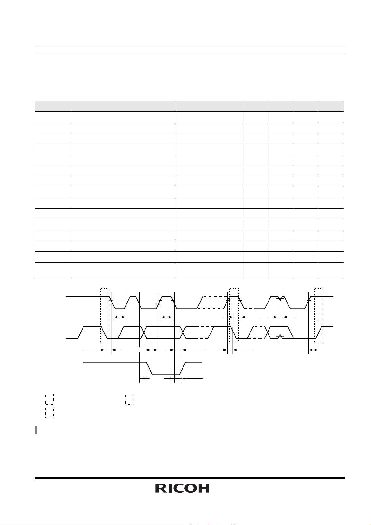
RS5C372A
AC CHARACTERISTICS
• VDD≥1.7V (supports standard mode I
Unless otherwise specified : VSS=0V, Topt=−40 to +85, Crystal=32.768kHz or 32.000kHz,
Symbol Item Conditions Min. Typ. Max. Unit
fSCL SCL Clock Frequency 0 100 kHz
2
C bus)
Input and Output Conditions:VIH=0.8×VDD,VIL=0.2×VDD,VOL=0.2×VDD,CL=50pF
tLOW SCL Clock “L” Time 4.7
tHIGH SCL Clock “H” Time 4.0
tHD ; STA Start Condition Hold Time 4.0
tSU ; STO Stop Condition Setup Time 4.0
tSU ; STA Start Condition Setup Time 4.7
μs
μs
μs
μs
μs
tSU ; DAT Data Setup Time 250 ns
tHDH ; DAT “H”Data Hold Time 0 ns
tHDL ; DAT “L”Data Hold Time
tHDL ; DAT “L”Data Hold Time
tPL ; DAT
tPZ ; DAT
tR
tF
tSP
SDA “L”Stable Time After Falling of SCL
SDA off Stable Time After Falling of SCL
Rising Time of SCL and SDA (Input)
Falling Time of SCL and SDA (Input)
Spike Width that can be Removed
with Input Filter
V
DD≥2.0V
V
DD≥1.7V
2.0
2.0
1000 ns
300 ns
50 ns
35 ns
150 ns
μs
μs
SSrP
SCL
t
SDA(IN)
t
HD;STA
SDA(OUT)
Start condition
S
Sr
Repeated start condition
LOW
t
SU;DAT
t
PL;DAT
Stop condition
P
t
HIGH
t
HDH;DAT
t
HDL;DAT
t
PZ;DAT
∗) For detailed information refer to “USAGES, 1.2 Transmission System of I
t
SU;STA
t
HD;STA
2
C bus.”
t
SP
t
SU;STO
5

RS5C372A
• VDD≥2.5V (supports fast mode I
Unless otherwise specified : VSS=0V, Topt=−40 to +85, Crystal=32.768kHz or 32.000kHz,
Symbol Item Conditions Min. Typ. Max. Unit
fSCL SCL Clock Frequency 0 400 kHz
2
C bus)
Input and Output Conditions:VIH=0.8×VDD,VIL=0.2×VDD,VOL=0.2×VDD,CL=50pF
tLOW SCL Clock “L” Time 1.3
tHIGH SCL Clock “H” Time 0.6
tHD ; STA Start Condition Hold Time 0.6
tSU ; STO Stop Condition Setup Time 0.6
tSU ; STA Start Condition Setup Time 0.6
μs
μs
μs
μs
μs
tSU ; DAT Data Setup Time 100 ns
tHDH ; DAT “H”Data Hold Time 0 ns
tHDL ; DAT “L”Data Hold Time 35 ns
tPL ; DAT
tPZ ; DAT
tR
tF
tSP
SDA “L” Stable Time After Falling of SCL
SDA off Stable Time After Falling of SCL
Rising Time of SCL and SDA (Input)
Falling Time of SCL and SDA (Input)
Spike Width that can be Removed
with Input Filter
0.9
0.9
300 ns
300 ns
50 ns
μs
μs
SSrP
SCL
t
t
LOW
t
HIGH
HD;STA
t
SP
SDA(IN)
t
HD;STA
SDA(OUT)
Start condition
S
Sr
Repeated start condition
t
SU;DAT
t
PL;DAT
Stop condition
P
t
HDH;DAT
t
HDL;DAT
t
PZ;DAT
∗) For detailed information refer to “USAGES, 1.2 Transmission System of I
t
SU;STA
2
C bus.”
t
SU;STO
6

RS5C372B
I2C bus SERIAL INTERFACE REAL-TIME CLOCK IC
OUTLINE
The RS5C372B is a CMOS type real-time clock which is connected to the CPU via 2-wires and capable of
serial transmission of clock and calendar data to the CPU.
The RS5C372B can generate various periodic interrupt clock pulses lasting for long period (one month), and
alarm interrupt can be made by days of the week, hours, and minutes by two incorporated systems. Since an
oscillation circuit is driven at a constant voltage, it undergoes fluctuations of few voltage and conseq uent ly offers
low current consumption (T yp. 0.5μA at 3V). It also provides an oscillator halt sensing function applicable for data
validation at power-on and other occasions and 32-kHz clock output for an external micro computer. (CMOS
output) The product also incorporates a time trimming circuit that adjusts the clock with higher precision by
adjusting any errors in crystal oscillator frequencies based on signals from the CPU. The crystal oscillator may
be selected from 32.768kHz or 32.000kHz types. Integrated into an ultra compact and ultra thin 8 pin SSOP
package, the RS5C372B is the optimum choice for equipment requiring small sized and low power consuming
products.
FEATURES
• Time keeping voltage: 1.45V to 6.0V
• Lowest supply current: 0.5μA Typ. ..................(0.9μA Max.) : 3V (25°C)
..........................................................................(1.0μA Max.) : 3V (−40 to +85°C)
• Connected to the CPU via only 2-wires (I
• A clock counter (counting hours, minutes, and se conds) and a cal endar counter (co unting leap years, years,
months, days, and days of the week) in BCD codes
• Interrupt to the CPU (period of one month to one second, interrupt flag, interrupt halt function) (
• Two systems of alarm functions (days of the week, hours, and minutes) (
• Oscillation halt sensing to judge internal data validity
• Clock output of 32.768kHz (32.000kHz) (output controllable via a register) ⋅⋅⋅⋅⋅⋅⋅(CMOS output)
• Second digit adjustment by ±30 seconds
• Automatic leap year recognition up to the year 2099
• 12-hour or 24-hour time display selectable
• Oscillation stabilizing capacity (C
• High precision time trimming circuit
• Oscillator of 32.768kHz or 32.000kHz may be used
• CMOS logic
• Package: 8pin SSOP
G, CD) incorporated
2
C bus Interface, Max.400kHz, address 7bit)
INTR
)
INTR
)
7
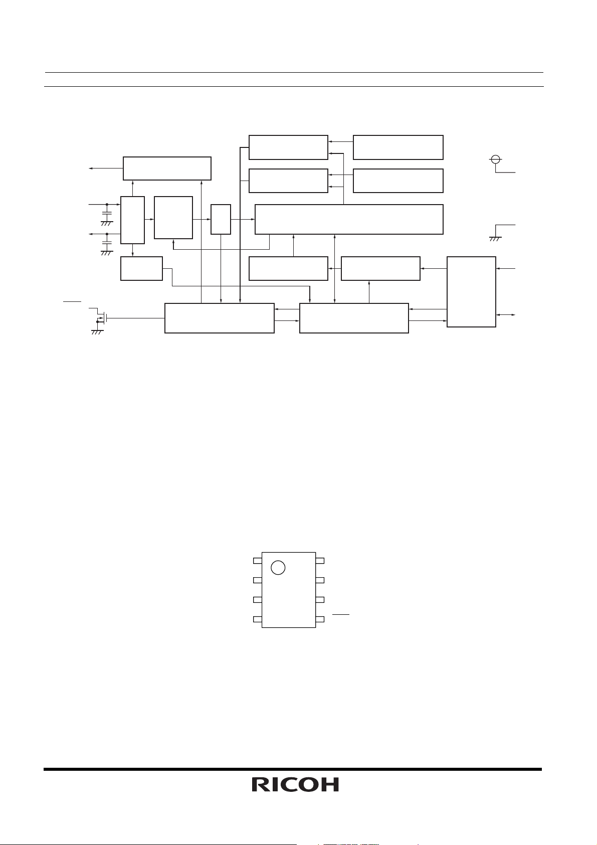
RS5C372B
A
BLOCK DIAGRAM
32KOUT
32kHz OUTPUT
CONTROL
COMPARATOR_A
COMPARATOR_B
ALARM_A REGISTER
(WEEK,MIN,HOUR)
ALARM_B REGISTER
(WEEK,MIN,HOUR)
VDD
OSCIN
OSC
OSCOUT
DETECT
INTR
OSC
DIVIDER
CORREC
-TION
INTERRUPT CONTROL
DIV
(SEC,MIN,HOUR,WEEK,DAY,MONTH,YEAR)
ADDRESS
DECODER
TIME COUNTER
ADDRESS
REGISTER
SHIFT REGISTER
I/O
CONTROL
APPLICATIONS
• Communication devices (multi function phone, portable phone, PHS or pager)
• OA devices (f ax, portable fax)
• Computer (desk-top and mobile PC, portable word-proce ssor, PDA, electric note or video game)
• AV components (portable audio unit, video camera,camera, digital camera or remote controller)
• Home appliances (rice cooker, electric oven)
• Other(car navigation system,multi-function watch)
V
SS
SCL
SD
PIN CONFIGURATION
32KOUT
SCL
SDA
V
SS
• 8pin SSOP
1
2
3
4
8
7
6
5
V
DD
OSCIN
OSCOUT
INTR
8
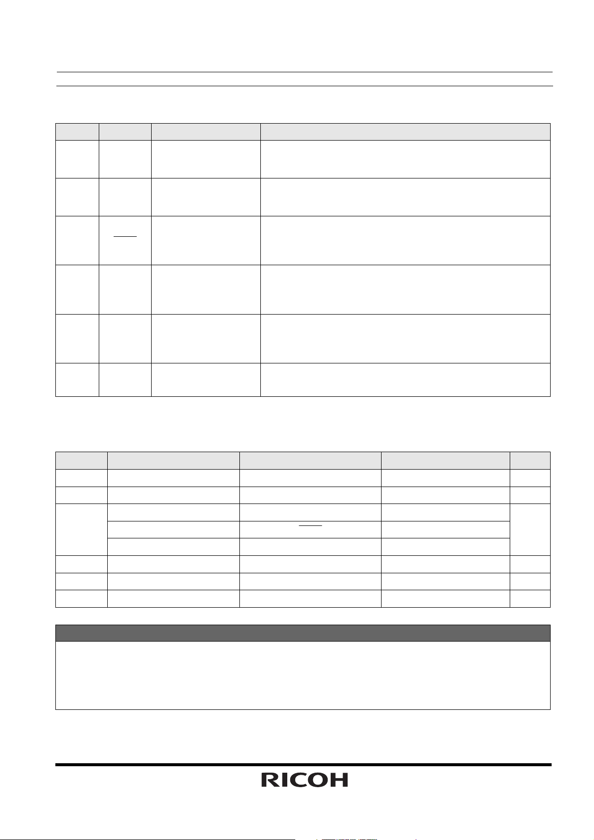
PIN DESCRIPTIONS
Pin No.
2 SCL
Symbol Name Description
Serial Clock Line
3 SDA
Serial Data Line
5
1
7
6
INTR
32KOUT
OSCIN
OSCOUT
Interrupt Output
32-kHz Clock Output
Oscillator Circuit
Input/Output
8
4
VDD
V
SS
Positive Power Supply Input
Negative Power Supply Input
RS5C372B
This pin is used to input shift clock pulses to synchronize data
input/output to and from the SDA pin with this clock. Up to 6V
beyond V
This pin inputs and outputs written or read data in synchronization
may be input.
DD
with shift clock pulses from the SCL pin. Up to 6V beyond V
be input. This pin functions as an Nch open drain output.
This pin outputs periodic interrupt pulses and alarm interrupt
(Alarm_A, Alarm_B) to the CPU. This pin is off when power is
activated from 0V. This pin functions as an Nch open drain
output.
The 32KOUT pin is used to output 32.768kHz clock pulses(when
32.768kHz crystal is used).Enabled at power-on from 0volts.
CMOS output. The RS5C372B can disable 32-kHz clock output
in response to a command from the host computer.
These pins configure an oscillator circuit by connecting a
32.768kHz or 32.000kHz crystal oscillator between the OSCIN
-OSCOUT pins. (Any other oscillator circuit components are
built into the RS5C372A.)
The VDD pin is connected to the positive power supply and VSS
to the ground.
DD may
ABSOLUTE MAXIMUM RATINGS
(VSS=0V)
Symbol Item Conditions Ratinge Unit
VDD Supply Voltage
VI Input Voltag SCL, SDA
Output Voltage 1 SDA
VO
Output Voltage 2
Output Voltage 3 32KOUT
PD Power Dissipation
Topt=25°C
Topt Operating Temperature
Tstg Storage Temperature
INTR
−0.3 to +7.0
−0.3 to +7.0
−0.3 to +7.0
−0.3 to +12
−0.3 to V
DD+0.3
300 mW
−40 to +85 °C
−55 to +125 °C
ABSOLUTE MAXIMUM RATINGS
Absolute Maximum ratings are threshold limit values that must not be exceeded even for an instant under
any conditions. Moreover, such values for any two items must not be reached simultaneously. Operation
above these absolute maximum ratings may cause degradation or permanent damage to the device.
These are stress ratings only and do not necessarily imply functional operation below these limits.
V
V
V
9
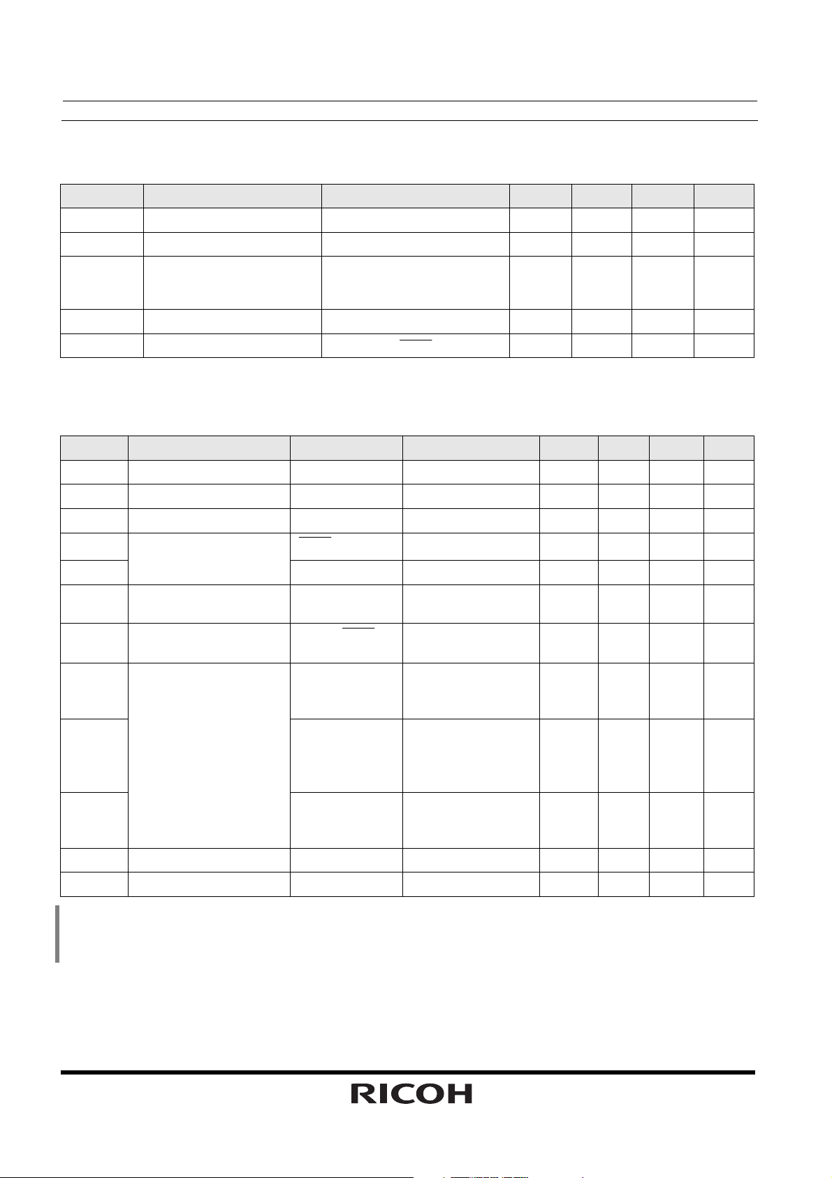
RS5C372B
RECOMMENDED OPERATING CONDITIONS
(Vss=0V,Topt=−40 to +85°C)
Symbol Item Conditions Min. Typ. Max. Unit
VDD Supply Voltage 2.0 6.0 V
VCLK Timekeeping Voltage 1.45 6.0 V
32.768
FXT Oscillation Frequency
or
32.000
VPUP1 Pull-up Voltage 1 SCL, SDA 6.0 V
kHz
VPUP2 Pull-up Voltage 2
INTR
10.0 V
DC CHARACTERISTICS
Unless otherwise specified: Vss=0V, VDD=3V, Topt=−40 to +85°C, Oscillation frequency=32.768kHz, or 32.000kHz(R1=30kΩ)
Symbol Item Pin name Conditions Min. Typ. Max. Unit
VIH “H” Input Voltage SCL, SDA 0.8VDD 6.0 V
VIL “L” Input Voltage SCL, SDA
IOH “H” Output Current 32KOUT
INTR
SDA
32KOUT
,
IOL1
IOL2
“L” Output Current
IILK Input Leakage Current SCL
IOZ
Output Off State
Leakage Current
SDA,
32KOUT
INTR
,
IDD1 VDD
IDD2 VDD
IDD3
CG
Standby Current
Internal Oscillation Capacitance 1
VDD
OSCIN 10 pF
V
OH=VDD−0.5V
V
OL1=0.4V
V
OL2=0.6V
V
I=6V or Vss
DD=6V
V
V
O=6V or Vss
DD=6V
V
DD=3V Topt=25°C
V
SCL, SDA=3V
Output=OPEN
DD=3V
V
Topt=−40 to +85°C
SCL, SDA=3V
Output=OPEN
DD=6V
V
SCL, SDA=6V
Output=OPEN
1
∗
1
∗
−0.3
-0.5 mA
1 mA
6 mA
−1
−1
0.5 0.9
1.0
0.8 2.0
0.2VDD V
1
1
μA
μA
μA
μA
μA
CD
Internal Oscillation Capacitance 2
OSCOUT 10 pF
∗1) The mode outputs no clock pulses when output is open (output off state).
For consumption current (output: no load) when 32kHz pulses are output from 32KOUT, see “USAGES, 6.
Typical Characteristic Measurements”
10
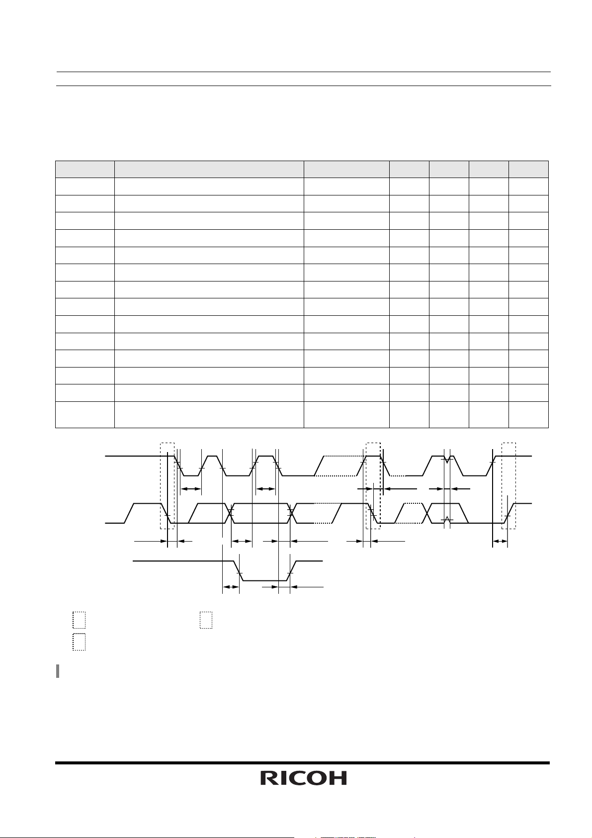
RS5C372B
AC CHARACTERISTICS
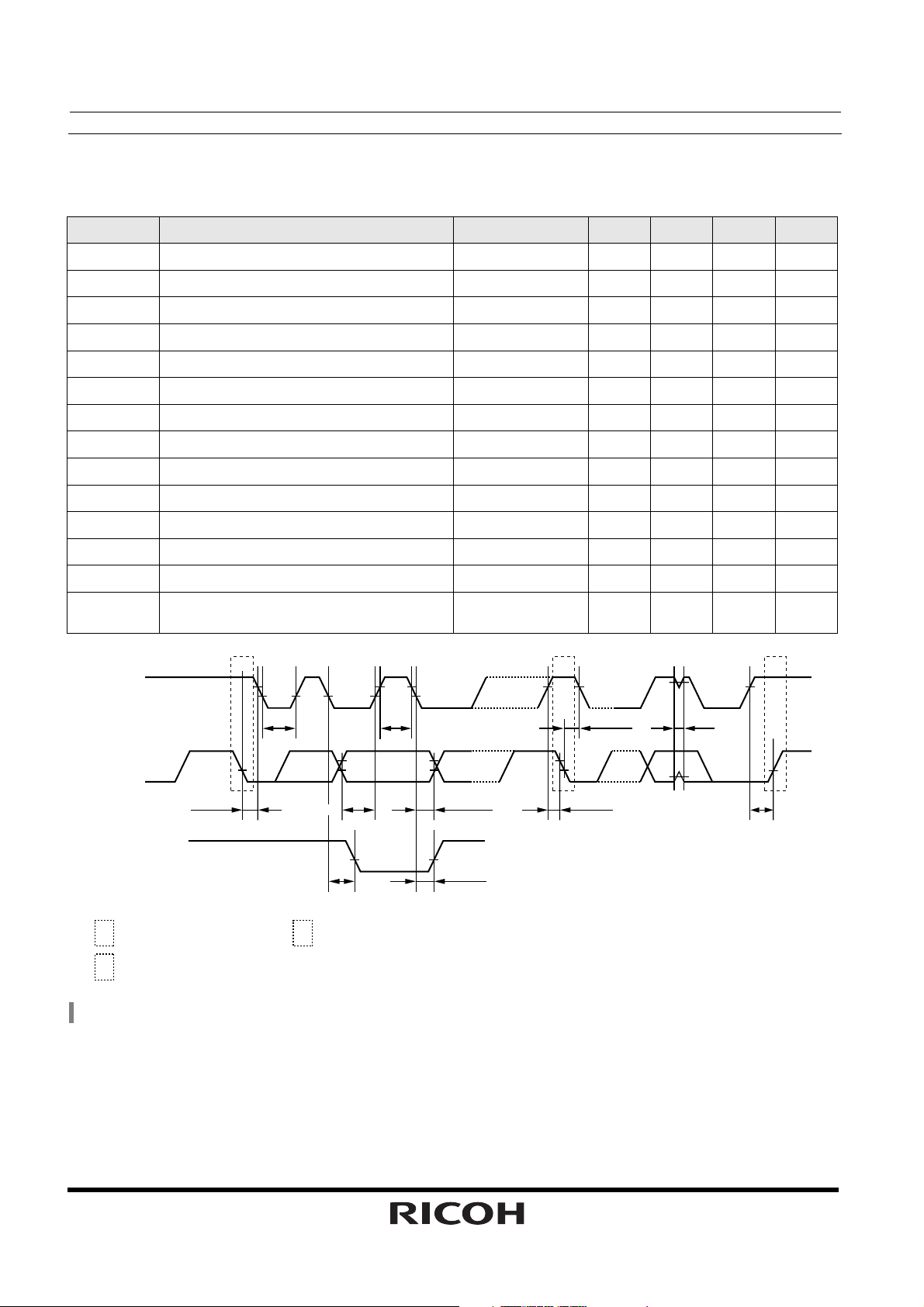
• VDD≥2.0V (supports standard mode I
Unless otherwise specified : VSS=0V, Topt=−40 to +85, Crystal=32.768kHz or 32.000kHz,
Symbol Item Conditions Min. Typ. Max. Unit
fSCL SCL Clock Frequency 0 100 kHz
2
C bus)
Input and Output Conditions:VIH=0.8×VDD,VIL=0.2×VDD,VOL=0.2×VDD,CL=50pF
tLOW SCL Clock “L” Time 4.7
tHIGH SCL Clock “H” Time 4.0
tHD ; STA Start Condition Hold Time 4.0
tSU ; STO Stop Condition Setup Time 4.0
tSU ; STA Start Condition Setup Time 4.7
μs
μs
μs
μs
μs
tSU ; DAT Data Setup Time 250 ns
tHDH ; DAT “H”Data Hold Time 0 ns
tHDL ; DAT “L”Data Hold Time 35 ns
tHDL ; DAT SDA “L”Stable Time After Falling of SCL 2.0
tPZ ; DAT
SDA Off Stable Time After Falling of SCL
2.0
μs
μs
tR Rising Time of SCL and SDA (Input) 1000 ns
tF Falling Time of SCL and SDA (Input) 300 ns
tSP
Spike Width that can be Removed with
Input Filter
50 ns
SSrP
SCL
t
t
LOW
t
HIGH
HD;STA
t
SP
SDA(IN)
t
HD;STA
SDA(OUT)
Start condition
S
Sr
Repeated start condition
t
SU;DAT
t
PL;DAT
Stop condition
P
t
HDH;DAT
t
HDL;DAT
t
PZ;DAT
∗) For detailed information refer to “USAGES, 1.2 Transmission System of I
t
SU;STA
2
C bus.”
t
SU;STO
11
RS5C372B
• VDD≥2.5V (supports fast mode I
Unless otherwise specified : VSS=0V, Topt=−40 to +85, Crystal=32.768kHz or 32.000kHz,
Symbol Item Conditions Min. Typ. Max. Unit
fSCL SCL Clock Frequency 0 400 kHz
2
C bus)
Input and Output Conditions:VIH=0.8×VDD,VIL=0.2×VDD,VOL=0.2×VDD,CL=50pF
tLOW SCL Clock “L” Time 1.3
tHIGH SCL Clock “H” Time 0.6
tHD ; STA Start Condition Hold Time 0.6
tSU ; STO Stop Condition Setup Time 0.6
tSU ; STA Start Condition Setup Time 0.6
μs
μs
μs
μs
μs
tSU ; DAT Data Setup Time 100 ns
tHDH ; DAT “H”Data Hold Time 0 ns
tHDL ; DAT “L”Data Hold Time 35 ns
tPL ; DAT
tPZ ; DAT
SDA “L” Stable Time After Falling of SCL
SDA Off Stable Time After Falling of SCL
0.9
0.9
μs
μs
tR Rising Time of SCL and SDA (Input) 300 ns
tF Falling Time of SCL and SDA (Input) 300 ns
tSP
Spike Width that can be Removed with
Input Filter
50 ns
SSrP
SCL
t
t
LOW
t
HIGH
HD;STA
t
SP
SDA(IN)
t
HD;STA
SDA(OUT)
Start condition
S
Sr
Repeated start condition
t
SU;DAT
t
PL;DAT
Stop condition
P
t
HDH;DAT
t
HDL;DAT
t
PZ;DAT
∗) For detailed information refer to “USAGES, 1.2 Transmission System of I
t
SU;STA
2
C bus.”
t
SU;STO
12

RS5C372A/B
GENERAL DESCRIPTION
1. Interfacing with the CPU
The RS5C372A/B read/write data over I2C bus interface via 2-wires: SDA (data) and SCL (clock). Since the
output of the I/O pin of SDA is open d rain, dat a interfacing with a CPU with dif fere nt supply volt age i s possible by
applying pull-up resistor on the circuit board. The maximum clock frequency of 400kHz of SCL enables data
transfer in I
2. Clock function
The clock function of the RS5C372A/B allows write/read data from lower two digits of the dominical year to
seconds to and from the CPU. When lower two digits of the dominical year are multiples of 4, the year is
recognized as a leap year automatically. Up to the year 2099 leap years will be automatically recognized.
∗) The year 2000 is a leap year while the year 2100 is not.
3. Alarm function
⋅ RS5C372A
2
C bus fast mode.
The RS5C372A has an ala rm function that outputs an interrupt sign al from
CPU when the day of the week, hour or minute corresponds to the setting. These two systems of alarms
(Alarm_A, Alarm_B), each may output interrupt signal separately at a specified time. The alarm may be
selectable between on and of f for each day of the wee k, thus allowi ng outputting alarm everyd ay or on a sp ecifi c
day of the week. The Alarm_A is output from the
INTRB
or the
Polling is possible separately for each alarm function.
pins.
INTRA
pin while the Alarm_B is output from either the
INTRA
INTRB
or
output pins to the
INTRA
⋅ RS5C372B
The RS5C372B has an alarm function that outputs an interrupt signal from
the day of the week, hour or minute corresponds to the setting. These two systems of alarms (Alarm_A,
Alarm_B), each may output interrupt signal separately at a specified time. The alarm may be select able b etween
on and off for each day of the week, thus allowing outputting alarm everyday or on a specific day of the week.
Polling is possible separately for each alarm function.
4. High precision time trimming function
The RS5C372A/B have an internal oscillation circuit capacitance CG and CD so that an oscillation circuit may
be configured simply by externally connecting a crystal. Either 32.768kHz or 32.000kHz may be selected as a
crystal oscillator by setting the internal register appropriately. The RS5C372A/B incorporate a time trimming
circuit that adjusts gain or loss of the clock from the CPU up to approx. ±189ppm (±194ppm when 32.000kHz
crystal is used) by approximately 3ppm steps to correct discrepancy in oscillation frequency.
(Error after correction: ±1.5ppm: 25°C)
Thus by adjusting frequencies for each system,
INTR
output pin to the CPU when
⋅ Clock display is possible at much higher precision than conventional real-time clock while using a crystal with
broader fluctuation in precision.
⋅ Even seasonal frequency fluctuation may be corrected by adjusting seasonal clock error.
⋅ For those systems that have temperature detection precision of clock function may be increased by correcting
clock error according to temperature fluctuations.
13
RS5C372A/B
5. Oscillation halt sensing
The oscillation halt sensing function uses a register to store oscillation halt information. This function may be
used to determine if the RS5C372A/B supply power has been booted from 0V and if it has been backed up.
This function is useful for determining if clock data is valid or invalid.
6. Periodic interrupt
⋅ RS5C372A
The RS5C372A can output periodic interrupt pulses in addition to alarm function from the
pins.
This frequency may be selected from 2Hz (every 0.5 seconds), 1Hz (every second), 1/60Hz (every minute),
1/3600Hz (every hour) and monthly (1st of month).
Output wave form for periodic interrupt may be selected from regular pulse waveform (2Hz and 1Hz) and
waveforms (every second, every minute, every hour and every month) that are appropriate for CPU level
interrupt. Outputs may be selected either
pin status in the register.
INTRA
or
INTRB
. The RS5C372A has polling function that monitors
INTRA
and
INTRB
⋅ RS5C372B
The RS5C372B can output periodic interrupt pulses in addition to alarm function from the
frequency may be selected from 2Hz (every 0.5 secon ds), 1Hz (every second), 1/60H z (every minute), 1/3600Hz
(every hour) and monthly (1st of month).
Output wave form for periodic interrupt may be selected from regular pulse waveform (2Hz and 1Hz) and
waveforms (every second, every minute, every hour and every month) that are appropriate for CPU level
interrupt. Periodic Interrupt outputs from
the register.
INTR
. The RS5C372B has polling function that monitors pin status in
7. 32-kHz clock output
INTR
pin. This
⋅ RS5C372A
The RS5C372A may output oscillation frequency from the
which is set to on or off by setting the register.
INTRB
pin. This clock output is set for output by default,
⋅ RS5C372B
The RS5C372B may output oscillation frequency from the 32KOUT pin. This clock output is set for output by
default, which is set to on or off by setting the register. The 32KOUT pin is CMOS push-pull output terminal.
Note
The year-digit counter of RS5C372A/B counts only lower two digits of a year and no counter is supplied for
upper two digits. When you are going to use this product in a system that must cope with “2000 year
problem” which shall be corrected by software.
14
RS5C372A/B
A
A
A
FUNCTIONAL DESCRIPTIONS
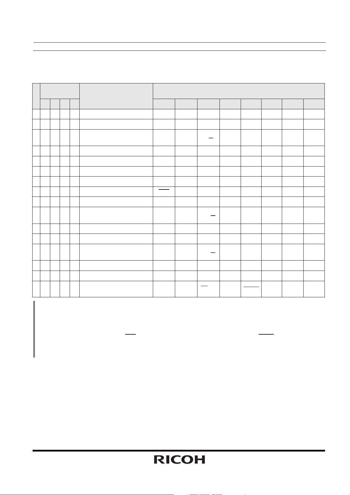
1. Allocation of Internal Addresses
Internal
address
3 A2 A1 A0
A
0 0 0 0 0 Second Counter
Contents
D7 D6 D5 D4 D3 D2 D1 D0
2
—
∗
40 S20 S10 S8 S4 S2 S1
S
1 0 0 0 1 Minute Counter — M40 M20 M10 M8 M4 M2 M1
H
2 0 0 1 0 Hour Counter — —
P/
20
H10 H8 H4 H2 H1
3 0 0 1 1 Day of the Week Counter — — — — — W4 W2 W1
4 0 1 0 0 Day Counter — — D20 D10 D8 D4 D2 D1
Data
1
∗
5 0 1 0 1 Month Counter
— — — MO10 MO8 MO4 MO2 MO1
6 0 1 1 0 Year Counter Y80 Y40 Y20 Y10 Y8 Y4 Y2 Y1
7 0 1 1 1 Time Trimming Register
XSL
F6 F5 F4 F3 F2 F1 F0
8 1 0 0 0 Alarm_A (Minute Register) — AM40 AM20 AM10 AM8 AM4 AM2 AM1
AH
9 1 0 0 1 Alarm_A (Hour Register) — —
A 1 0 1 0
B 1 0 1 1
Alarm_A (Day of the W e ek R e gi s te r )
Alarm_B (Minute Register)
— AW6 AW5 AW4 AW3 AW2 AW1 AW0
— BM40 BM20 BM10 BM8 BM4 BM2 BM1
C 1 1 0 0 Alarm_B (Hour Register) — —
D 1 1 0 1
Alarm_B (Day of the W e ek R e gi s te r )
— BW6 BW5 BW4 BW3 BW2 BW1 BW0
E 1 1 1 0 Control Register 1 AALE BALE
F 1 1 1 1 Control Register 2 — —
AP/
BH
BP/
SL
12
20
AH10 AH8 AH4 AH2 AH1
20
BH10 BH8 BH4 BH2 BH1
∗
2
/24
5
SL1
ADJ
XSTP
5
∗
∗
∗
3
4
TEST
CLEN
CT2 CT1 CT0
CTFG AAFG BAFG
∗1) All the listed data can be read and written except for ADJ/XSTP.
∗2) The “–” mark indicates data which can be read only and set to “0” when read.
∗3) The ADJ/XST P bit of the control register2 is set to ADJ for write and XSTP for read operation. The XSTP bit
is set to “0” by writing data into the control register2 for normal oscillation.
∗4) When XSTP is set to “1”, the
XSL
, F6 to F0, CT2 to CT0, AALE, BALE, SL2, SL1,
CLEN
and TEST bits are
reset to “0”.
∗5) SL1 and SL2 apply to the RS5C372A. For the RS5C372B, these bits must be filled with “0”.
15
RS5C372A/B
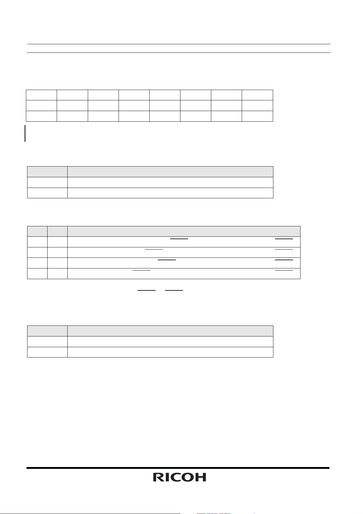
2. Registers
2.1 Control Register 1 (at internal address Eh)
D7 D6 D5 D4 D3 D2 D1 D0
2
AALE BALE
AALE BALE
SL
SL
∗
2
SL1
2
∗
2
SL1
0 0 0 0 0 0 0 0
2
∗
2
∗
TEST CT
TEST CT
2 CT1 CT0
2 CT1 CT0
(For write operation)
(For read operation)
Default
∗1) The default means read value when XSTP bit is set to “1” by starting up from 0V, or supply voltage drop, etc.
∗2) SL1 and SL2 apply to the RS5C372A. For the RS5C372B, these bits must be filled with “0”.
2.1-1 AALE, BALE
Alarm_A, Alarm_B enable bits
AALE, BALE Description
0 Alarm_A (Alarm_B) Correspondence action invalid (Default)
1 Alarm_A (Alarm_B) Correspondence action valid
2.1-2 SL2, SL1 (RS5C372A only)
Interrupt output select bits
SL2 SL1 Description
∗
0 0
0 1
1 0
1 1
Outputs Alarm_A, Alarm_B, INT to the
Outputs Alarm_A, INT to the
Outputs Alarm_A, Alarm_B to the
Outputs Alarm_A to the
INTRA
INTRA
INTRA
. Outputs 32k clock pulses, Alarm_B, INT to the
INTRA
. Outputs 32k clock pulses to the
. Outputs 32k clock pulses, Alarm_B to the
. Outputs 32k clock pulses, INT to the
INTRB
INTRB
INTRB
INTRB
(Default)
.
.
.
.
By setting SL1 and SL2 bits, two alarm pulses (Alarm_A and alarm_B), periodic interrupt output (INT),
32k clock pulses may be output to the
INTRA
or
INTRB
pins selectively.
2.1-3 TEST
Test bit
TEST Description
0 Ordinary operation mode (Default)
1 Test mode
The test bit is used for IC test. Set the TEST bit to 0 in ordinary operation.
16
RS5C372A/B
2.1-4 CT2, CT1, CT0
Periodic interrupt cycle select bit
CT2 CT1 CT0
Wave Form Mode
0 0 0 — off (“H”) (Default)
0 0 1 — Fixed at “L”
0 1 0 Pulse Mode 2Hz (Duty50%)
0 1 1 Pulse Mode 1Hz (Duty50%)
1 0 0 Level Mode Every second (synchronized with second count up)
1 0 1 Level Mode Every minute (00 second of every minute)
1 1 0 Level Mode Every hour (00 minute(s) 00 second(s) of every hour)
Description
Cycle and Falling Timing
1 1 1 Level Mode
Every month (the 1st day 00 A.M. 00 minute(s) 00 second(s) of every month)
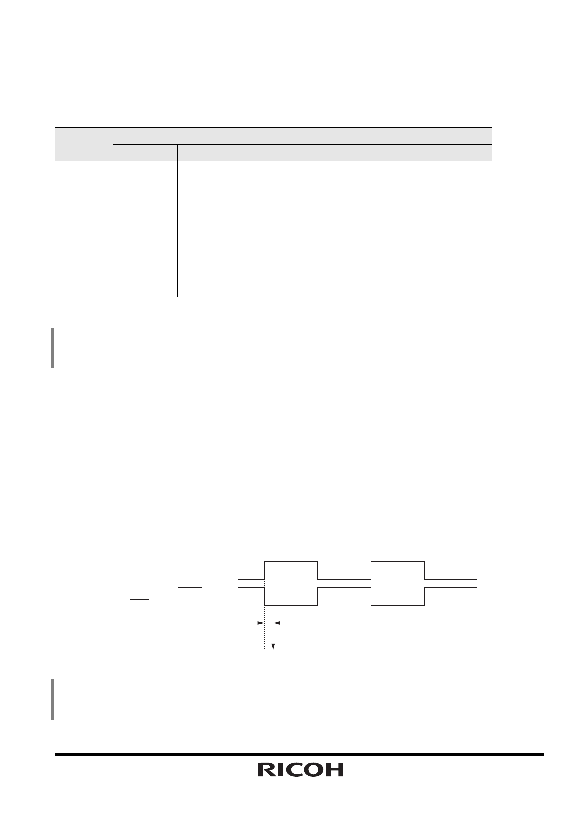
1) Pulse mode : Outputs 2Hz, 1Hz clock pulses. For relationships with counting up of seconds see the diagram
below.
∗) When 32.000kHz crystal is used,
In the 2Hz clock pulse mode, 0.496s clock pulses and 0.504s clock pulse are output alternately.
Duty cycle for 1Hz clock pulses becomes 50.4% (“L” duration is 0.496s while “H” duration is 0.504s).
2) Level mode : One second, one minute or one month may be selected for an interrupt cycle.
Counting up of seconds is matched with falling edge of interrupt output.
3) When the time trimming circuit is used, periodic interrupt cycle changes every 20 seconds.
Pulse mode : “L” duration of output pulses may change in the maximum range of ±3.784ms
(±3.875ms when 32.000kHz crystal is used.)
For example, Duty will be 50±0.3784% (or 50±0.3875% when 32.000kHz cryst al is used)
at 1Hz.
Level mode : Frequency in one second may change in the maximum range of ±3.784ms
(±3.875ms when 32.000kHz crystal is used.)
Relation Between Mode Waveforms and CTFG Bit
• Pulse mode
CTFG bit
INTRA or INTRB pins
(INTR pin for the RS5C372B)
Approx. 92μs (32.768kHz crystal is used)
Approx. 94μs (32.000kHz crystal is used)
(Counting up of seconds)
∗) Since counting up of seconds and the falling edge has a time lag of approx. 92μs (at 32.768kHz) (approx.
94μs when 32.000kHz crystal is used), time with apparently approx. one second of delay from time of the
real-time clock may be read when time is read in synchronization with the falling edge of output.
17
 Loading...