

RICOH RS5C321B Datasheet

ULTRA-COMPA CT SERIAL REAL-TIME CLOCK ICs
WITH 32.768kHz
RS5C321A/B
ELECTRONIC DEVICES DIVISION
NO.EA-040-9908
APPLICATION MANUAL

NOTICE
1. The products and the product specifications described in this application manual are subject to change or discontinuation of production without notice for reasons such as improvement. Therefore, before deciding to use
the products, please refer to Ricoh sales representatives for the latest information thereon.
2. This application manual may not be copied or otherwise reproduced in whole or in part without prior written consent of Ricoh.
3. Please be sure to take any necessary formalities under relevant laws or regulations before exporting or otherwise taking out of your country the products or the technical information described herein.
4. The technical information described in this application manual shows typical characteristics of and example
application circuits for the products. The release of such information is not to be construed as a warranty of or a
grant of license under Ricoh's or any third party's intellectual property rights or any other rights.
5. The products listed in this document are intended and designed for use as general electronic components in
standard applications (office equipment, computer equipment, measuring instruments, consumer electronic
products, amusement equipment etc.). Those customers intending to use a product in an application requiring
extreme quality and reliability, for example, in a highly specific application where the failure or misoperation of
the product could result in human injury or death (aircraft, spacevehicle, nuclear reactor control system, traffic
control system, automotive and transportation equipment, combustion equipment, safety devices, life support
system etc.) should first contact us.
6. We are making our continuous effort to improve the quality and reliability of our products, but semiconductor
products are likely to fail with certain probability. In order prevent any injury to persons or damages to property
resulting from such failure, customers should be careful enough to incorporate safety measures in their design,
such as redundancy feature, fire-containment feature and fail-safe feature. We do not assume any liability or
responsibility for any loss or damage arising from misuse or inappropriate use of the products.
7. Anti-radiation design is not implemented in the products described in this application manual.
8. Please contact Ricoh sales representatives should you have any questions or comments concerning the products or the technical information.
June 1995

OUTLINE
......................................................................................................
1
FEATURES
....................................................................................................
1
BLOCK DIAGRAM
.........................................................................................
2
APPLICATIONS
.............................................................................................
2
PIN CONFIGURATION
...................................................................................
2
PIN DESCRIPTIONS
......................................................................................
3
ABSOLUTE MAXIMUM RATINGS
...................................................................
4
RECOMMENDED OPERATING CONDITIONS
.................................................
4
DC CHARACTERISTICS
................................................................................
5
AC CHARACTERISTICS
................................................................................
5
TIMING CHARTS
...........................................................................................
6
FUNCTIONAL DESCRIPTIONS
......................................................................
7
1. Addressing
.................................................................................................
7
2. Registers
...................................................................................................
8
3. Counters
..................................................................................................
11
USAGES
......................................................................................................
13
1. Read Data (For the RS5C321A)
......................................................................
13
2. Write Data (For the RS5C321A)
.......................................................................
14
3. Read Data (For the RS5C321B)
......................................................................
15
4. Write Data (For the RS5C321B)
.......................................................................
16
5. CE Pin
....................................................................................................
17
6. Configuration of Oscillating Circuit
....................................................................
18
7. Oscillator Halt Sensing
.................................................................................
19
8. Typical Power Supply Circuit
...........................................................................
20
9. Oscillation Frequency Adjustment
.....................................................................
20
10. 32.768kHz Clock Output
..............................................................................
22
RS5C321A/B
APPLICATION MANUAL
CONTENTS

11. Typical Application
.....................................................................................
22
12. Typical Characteristic Measurements
...............................................................
23
13. Typical Software-based Operations
.................................................................
25
PACKAGE DIMENSIONS
..............................................................................
28
TAPING SPECIFICATION
..............................................................................
28

URTRA-COMPACT ALARM REAL-TIME
CLOCK ICs WITH 32.768kHz
1
RS5C321A/B
OUTLINE
The RS5C321A/B are CMOS type real-time clock ICs which are connected to the CPU via three signal lines and
capable of serial transmission of clock and calendar data to the CPU.
The RS5C321A/B can generate 32.768kHz clock pulse controled by register. Driving an oscillation circuit at constant voltage, the circuit presents less fluctuations in frequency and current consumption thank to its minimal voltage fluctuations consequently realizes low current consumption (0.6µA at 3V). It also provides an oscillator halt
sensing function for application to data validity at power-on and other occasions. Integrated into an ultra compact
and ultra thin 8pin SSOP (0.65mm pitch), the RS5C321A/B are the optimum choice for equipment requiring small
size and low power consumption.
The RS5C321A and the RS5C321B reads/writes data at falling and rising edge of serial clock respectively.
• Time keeping voltage 1.6V to 6.0V
• Lowest supply current 0.6µA TYP. (1.5µA MAX.) at 3V
• Connection to the CPU via only three pins: CE, SCLK/SCLK and SIO for addressing and data read/write
• A clock counter (counting hours, minutes, and seconds) and a calendar counter (counting leap years, years,
months, days, and days of the week) in BCD code
• 32.768kHz clock pulse controled by register.
• Oscillator halt sensing to judge internal data validity
• Second digit adjustment by ±30 seconds
• 12-hour or 24-hour time display selectable
• Automatic leap year recognition up to the year 2099
• CMOS logic
• Package: 8pin SSOP (0.65mm pitch)
FEATURES
APPLICATIONS
• Communication equipment (Multi-function telephone, portable telephone, PHS, pager)
• Business machines (Facsimile, portable facsimile)
• Personal computer (Desktop type, notebook type, word processor, PDA, electronic notebook, TV games)
• Audio visual equipment (Portable audio equipment, video camera, camera, digital camera, remote control equipment)
• Home use (Rice cooker, microwave range)
PIN CONFIGURATION
• 8pin SSOP (0.65mm pitch)
CE
1
SCLK
2
SIO
3
VSS
VDD
OSCIN
OSCOUT
RS5C321A RS5C321B
32KOUT
4
8
7
6
5
CE
1
SCLK
2
SIO
3
VSS
VDD
OSCIN
OSCOUT
32KOUT
4
8
7
6
5
RS5C321A/B
2
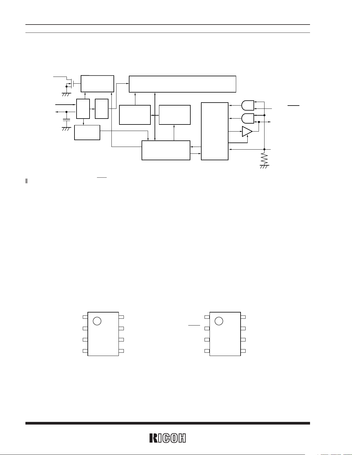
BLOCK DIAGRAM
OSC DIV
ADDRESS
DECODER
ADDRESS
REGISTER
TIME COUNTER
(SEC,MIN,HOUR,WEEK,DAY,MONTH,YEAR)
32kHz CLOCK
CONTORL
SHIFT REGISTER
I/O
CONTROL
OSC
DETECT
OSCIN
OSCOUT
SIO
SCLK/SCLK*
CE
32KOUT
*
) RS5C321A: SCLK RS5C321B: SCLK
RS5C321A/B
3
Pin No.
1
2
3
5
7
6
8
4
PIN DESCRIPTIONS
Symbol
CE
SCLK
(RS5C321A)
SCLK
(RS5C321B)
SIO
32KOUT
OSCIN
OSCOUT
VDD
VSS
Name
Chip enable input
Serial clock input
Serial input/output
32.768kHz clock
output
Oscillator circuit
input/output
Positive/Negative
power supply input
Description
The CE pin is used to interface the CPU and is accessible when held at the high
level. This pin is connected to a pull-down resistor. It should be switched to the
low level or opened when not accessed or when powering off the system.
This pin is used to input shift clock pulses to synchronize data input to, and output
from, the SIO pin. SCLK and SCLK are for writing data at falling and rising edge of
clock pulses respectively and also reading data at rising and falling edge of clock
pulses respectively.
The SIO pin inputs and outputs written or read data in synchronization with shift
clock pulses from the SCLK/SCLK pin. The SIO pin causes high impedance when
CE pin is held at the low level (CMOS input/output). After the CE pin is switched
to the high level and the control bits and the address bits are input from the SIO,
the SIO pin performs serial input and output operations.
The 32KOUT pin outputs 32.768kHz clock pulses when activated. This pin functions as an Nch open drain output.
These pins configure an oscillator circuit by connecting a 32.768kHz crystal oscillator between the OSCIN and OSCOUT pins and by connecting a capacitor between
the OSCIN and Vss pins. (Any other oscillator circuit components are built into
the RS5C321A/B.)
The VDD pin and V
SS pin are connected to the positive power supply and to the
ground level respectively.
RS5C321A/B
4
ABSOLUTE MAXIMUM RATINGS
ABSOLUTE MAXIMUM RATINGS
(VSS=0V)
Symbol Item Conditions Ratings Unit
VDD Supply voltage –0.3 to +7.0 V
VI Input voltage –0.3 to VDD+0.3 V
VO1 Output voltage 1 SIO –0.3 to VDD+0.3 V
VO2 Output voltage 2 32KOUT –0.3 to +12 V
PD Power dissipation Topt=25°C 300 mW
Topt Operating temperature –40 to +85 ˚C
Tstg Storage temperature –55 to +125 ˚C
Absolute Maximum ratings are threshold limit values that must not be exceeded even for an instant under
any conditions. Moreover, such values for any two items must not be reached simultaneously. Operation
above these absolute maximum ratings may cause degradation or permanent damage to the device. These
are stress ratings only and do not necessarily imply functional operation below these limits.
RECOMMENDED OPERATING CONDITIONS
(VSS=0V, Topt=–40 to +85˚C)
Symbol Item Conditions MIN. TYP. MAX. Unit
VDD Supply voltage 2.5 6.0 V
VCLK Time keeping voltage 1.6 6.0 V
fXT Oscillation frequency 32.768 kHz
CG External oscillation capacitance CL value of crystal=6 to 8pF 5 10 24 pF
V
PUP Pull-up voltage 32KOUT 10 V
RS5C321A/B
5
Symbol Item Pin name Conditions MIN. TYP. MAX. Unit
VIH “H” input voltage CE, SCLK/SCLK, SIO 0.8VDD VDD V
VIL “L” input voltage CE, SCLK/SCLK, SIO 0 0.2VDD V
IOH “H” output current SIO VOH=VDD –0.5V –0.5 mA
IOL1
“L” output current
SIO V
OL1=0.5V 0.5
mA
IOL2 32KOUT VOL2=0.4V 1
RDN Pull-down resistance CE 45 150 450 kΩ
IILK Input leakage current SCLK/SCLK VI=VDD or VSS –1 1 µA
IOZ1 Output off-state SIO VO=VDD or VSS –2 2
µA
IOZ2 leakage current 32KOUT VO=10V –5 5
I
DD1 Standby current 1* VDD
VDD=3V
0.6 1.5 µA
Input/Output: open
I
DD2 Standby current 2* VDD
VDD=6V
0.8 2.0 µA
Input/Output: open
C
D
Internal oscillation
OSCOUT 10 pF
capacitance
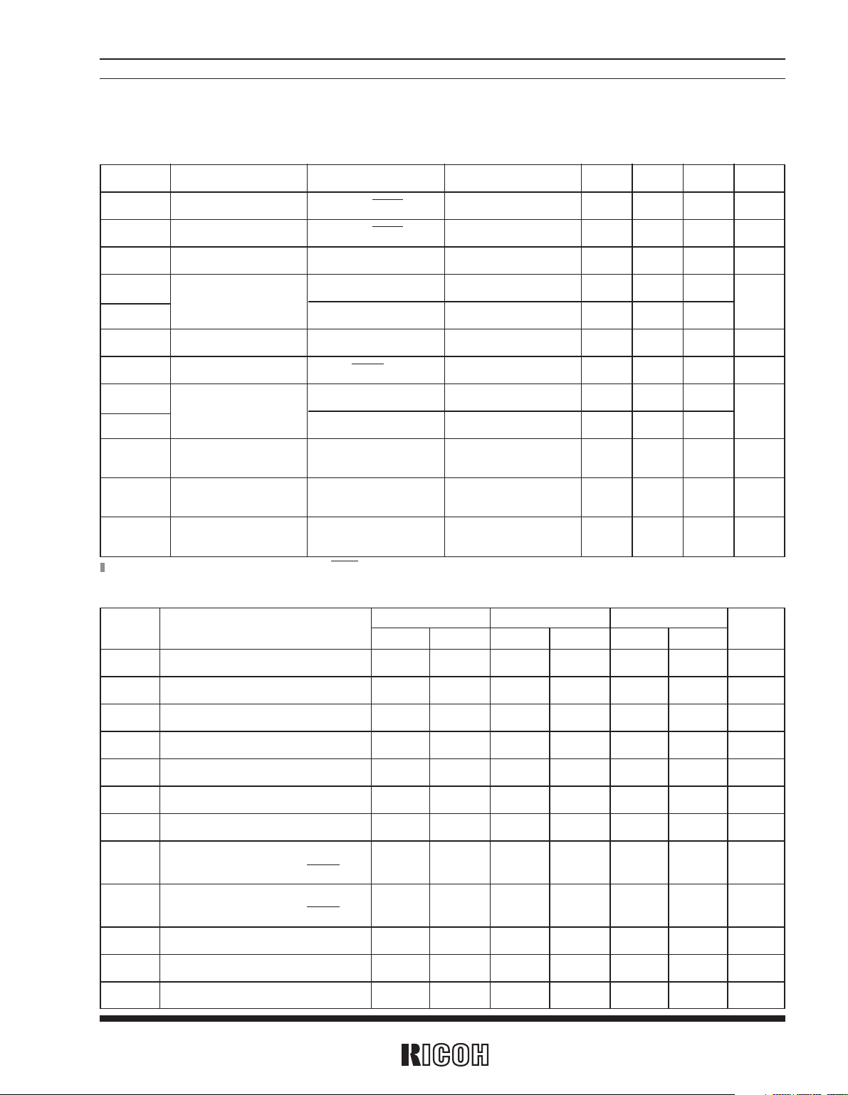
DC CHARACTERISTICS
Unless otherwise specified: VSS=0V, VDD=3V, Topt=–40 to +85˚C, Oscillation frequency=32.768kHz,(CL=6pF, R1=30kΩ), CG=10pF
AC CHARACTERISTICS
(VSS=0V, Topt=–40 to +85˚C, CL=50pF)
Symbol Item
V
DD≥4.5V VDD≥4.0V VDD≥2.5V
Unit
MIN. MAX. MIN. MAX. MIN. MAX.
tCES CE set-up time 175 200 400 ns
tCEH CE hold time 175 200 400 ns
tCR CE inactive time 350 400 800 ns
tSCK SCLK clock cycle time 350 400 800 ns
tCKH SCLK high time 175 200 400 ns
tCKL SCLK low time 175 200 400 ns
tCKS SCLK to CE set-up time 60 80 120 ns
tRE
Data output start time (from rising
120 135 300 ns
of SCLK) (from falling of SCLK)
tRR
Data output delay time (from rising
120 135 300 ns
of SCLK) (from falling of SCLK)
tRZ Output floating time 120 135 300 ns
tDS Input data set-up time 50 60 120 ns
tDH Input data hold time 50 50 80 ns
*
) IDD1, IDD2 is specified when 32kHz output is off (CLEN=1)
RS5C321A/B
6
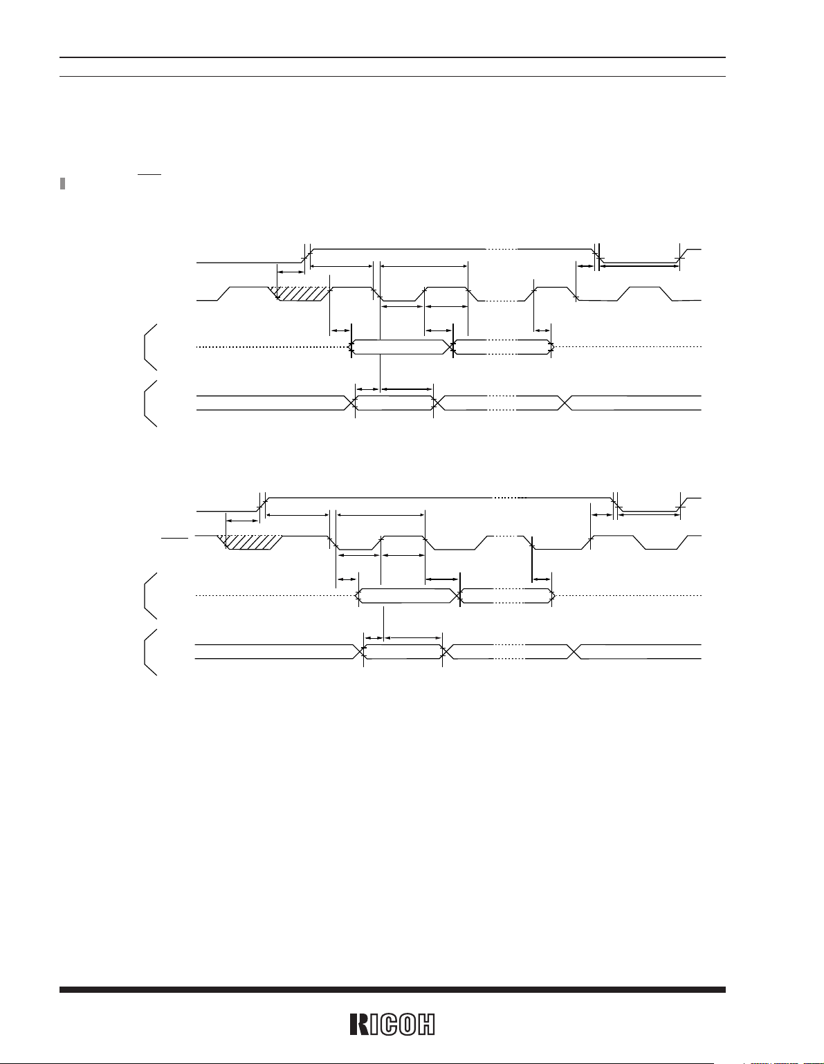
tSCKtCES
tCKS
tCEH
tCR
tRE
tRZ
tCKHtCKL
tRR
Read Data
Write Data
t
DS tDH
CE
SCLK
SIORead cycle
Write cycle
SIO
tSCKtCES
tCKS
tCEH
tCR
tRE
tRZ
tCKHtCKL
tRR
Read Data
Write Data
t
DS tDH
CE
SCLK
SIORead cycle
Write cycle
SIO
Input/Output conditions: VIH=0.8×VDD, VIL=0.2×VDD, VOH=0.8×VDD, VOL=0.2×VDD
• RS5C321A
• RS5C321B
TIMING CHARTS
*
) Any SCLK/SCLK state is allowed in the hatched area.
 Loading...