

RICOH RN5VS09AA-TL, RN5VS09AA-TR, RN5VS09AC, RN5VS09CA-TL, RN5VS13AA-TR Datasheet
...
ELECTRONIC DEVICES DIVISION
LOW VOLTAGE DETECTOR
RN5VS SERIES
APPLICATION MANUAL
NO.EA-037-9701

NOTICE
1. The products and the product specifications described in this application manual are subject to change or discontinuation of production without notice for reasons such as improvement. Therefore, before deciding to use
the products, please refer to Ricoh sales representatives for the latest information thereon.
2. This application manual may not be copied or otherwise reproduced in whole or in part without prior written consent of Ricoh.
3. Please be sure to take any necessary formalities under relevant laws or regulations before exporting or otherwise taking out of your country the products or the technical information described herein.
4. The technical information described in this application manual shows typical characteristics of and example
application circuits for the products. The release of such information is not to be construed as a warranty of or a
grant of license under Ricoh's or any third party's intellectual property rights or any other rights.
5. The products listed in this document are intended and designed for use as general electronic components in
standard applications (office equipment, computer equipment, measuring instruments, consumer electronic
products, amusement equipment etc.). Those customers intending to use a product in an application requiring
extreme quality and reliability, for example, in a highly specific application where the failure or misoperation of
the product could result in human injury or death (aircraft, spacevehicle, nuclear reactor control system, traffic
control system, automotive and transportation equipment, combustion equipment, safety devices, life support
system etc.) should first contact us.
6. We are making our continuous effort to improve the quality and reliability of our products, but semiconductor
products are likely to fail with certain probability. In order prevent any injury to persons or damages to property
resulting from such failure, customers should be careful enough to incorporate safety measures in their design,
such as redundancy feature, fire-containment feature and fail-safe feature. We do not assume any liability or
responsibility for any loss or damage arising from misuse or inappropriate use of the products.
7. Anti-radiation design is not implemented in the products described in this application manual.
8. Please contact Ricoh sales representatives should you have any questions or comments concerning the products or the technical information.
June 1995

OUTLINE
......................................................................................................
1
FEATURES
....................................................................................................
1
APPLICATIONS
.............................................................................................
1
BLOCK DIAGRAMS
.......................................................................................
2
TIME CHART
.................................................................................................
2
DEFINITION OF OUTPUT DELAY TIME tplh
....................................................
2
SELECTION GUIDE
.......................................................................................
4
PIN CONFIGURATION
...................................................................................
5
PIN DESCRIPTION
........................................................................................
5
ABSOLUTE MAXIMUM RATINGS
...................................................................
6
ELECTRICAL CHARACTERISTICS
.................................................................
7
ELECTRICAL CHARACTERITICS BY DETECTOR THRESHOLD
....................
10
OPERATION
................................................................................................
14
TEST CIRCUITS
...........................................................................................
15
TYPICAL CHARACTERISTICS
......................................................................
16
1) Supply Current vs. Input Voltage
...........................................................................
16
2) Detector Threshold vs. Temperature
.......................................................................
16
3) Output Voltage vs. Input Voltage
...........................................................................
17
4) Nch Driver Output Current vs. VDS
.........................................................................
18
5) Nch Driver Output Current vs. Input Voltage
................................................................
19
6) Pch Driver Output Current vs. Input Voltage
................................................................
20
7) Output Delay Time vs. Load Capacitance
..................................................................
20
8) Output Delay Time vs. Input Pin Capacitance
..............................................................
21
TYPICAL APPLICATIONS
............................................................................
22
• RN5VS××A CPU Reset Circuit(Nch Open Drain Output)
....................................................
22
• RN5VS××C CPU Reset Circuit(CMOS Output)
.............................................................
22
• RN5VS××A Output delay Time Circuit 1
.....................................................................
22
• RN5VS××A Output delay Time Circuit 2
.....................................................................
22
• Memory Back-up Circuit
.....................................................................................
22
• Voltage Level Indicator Circuit (lighted when the power runs out)
............................................
23
• Detector Threshold Changing Circuit
........................................................................
23
• Window Comparator Circuit
.................................................................................
23
• Excessive Charge Preventing Circuit
........................................................................
23
RN5VS SERIES
APPLICATION MANUAL
CONTENTS

PACKAGE DIMENSIONS
..............................................................................
25
TAPING SPECIFICATIONS
...........................................................................
25

LOW VOLTAGE DETECTOR
RN5VS SERIES
OUTLINE
The RN5VS Series are voltage detector ICs with high detector threshold accuracy and ultra-low supply current
by CMOS process, which can be operated at an extremely low voltage and is used, for instance, for system reset.
Each of these ICs consists of a voltage reference unit, a comparator, resistors for voltage detection, an output
driver and a hysteresis circuit. The detector threshold is fixed with high accuracy.
The RN5VS Series are operable by a lower voltage than that for the R
×5VL Series, and can be driven by a sin-
gle battery.
Two output types, Nch open drain type and CMOS type, are available. Since the package for these ICs are
SOT-23-5 (Mini-mold) package, high density mounting of the ICs on board is possible.
• Ultra-low Supply Current
............................
TYP. 0.8µA (V
DD=1.5V)
• Broad Operating Voltage Range
..................
0.7V to 10.0V (Topt =25˚C)
• Detector Threshold
........................................
Stepwise setting with a step of 0.1V in the range of 0.9V to 6.0V
is possible (refer to Selection Guide).
• High Accuracy Detector Threshold
..............
±3.0%
• Low Temperature-Drift Coefficien of Detector Threshold
..............
TYP. ±100ppm/˚C
• Two Output Types
.........................................
Nch Open Drain and CMOS
• Packages
.........................................................
SOT-23-5 (Mini-mold)
FEATURES
APPLICATIONS
•
CPU & Logic Circuit Reset
•
Battery Checker
•
Window Comparator
•
Wave Shaping Circuit
•
Battery Back-Up Circuit
•
Power Failure Detector
RN5VS
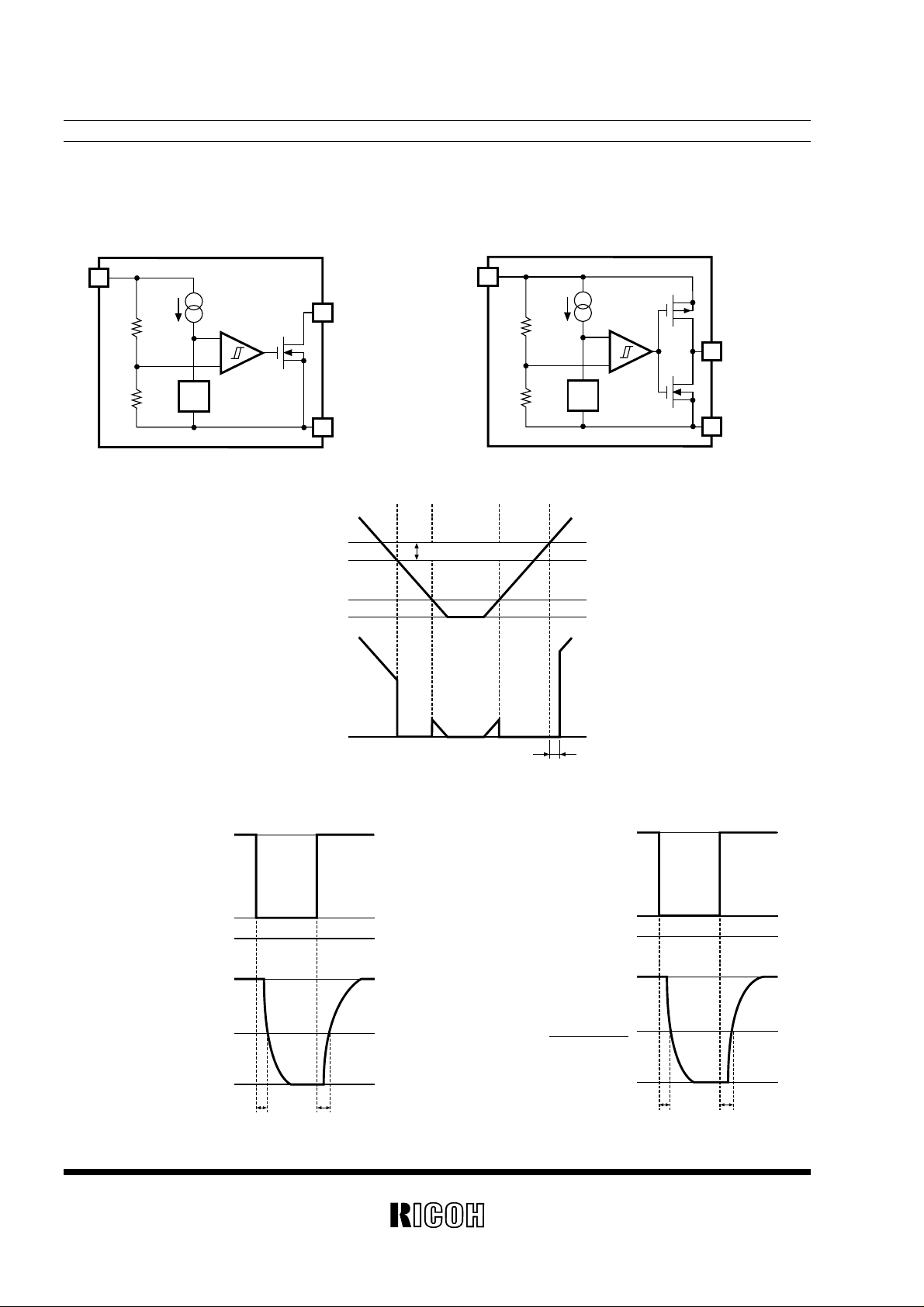
BLOCK DIAGRAMS
• Nch Open Drain Output (RN5VS××A) • CMOS Output (RN5VS××C)
TIME CHART
DEFINITION OF OUTPUT DELAY TIME tplh
2
3
Vref
OUT
GND
V
DD
–
+
1
VDD
2
1
3
Vref
OUT
GND
–
+
Detector Threshold Hysteresis
tPLH
Released Voltage +VDET
Detected Voltage –V
DET
Supply Voltage
(V
DD)
Output Voltage
(OUT)
Minimum Operating Voltage
GND
GND
tPLHtPHL
Input Voltage
(V
DD)
Output Voltage
Nch Open Drain Output
GND
GND
2.5V
5.0V
0.7V
+V
DET + 2.0V
tPLHtPHL
CMOS Output
GND
GND
0.7V
+V
DET + 2.0V
+V
DET +2.0V
+V
DET + 2.0V
2
Input Voltage
(V
DD)
Output Voltage

RN5VS
Output Delay Time tPLH is defined as follows:
1. In the case of Nch Open Drain Output:
When the time at which a pulse voltage which increases from 0.7V to +V
DET+2.0V is applied to VDD is Time A, and
the time at which the output voltage reaches 2.5V under the conditions that the output pin (OUT) is pulled up
to 5V by a resistor of 470kΩ is Time B, the time period from Time A through Time B.
2. In the case of CMOS Output:
When the time at which a pulse voltage which increases from 0.7V to +V
DET+2.0V is applied to VDD is Time A, and
the time at which the output voltage reaches the voltage of (+V
DET+2.0V)/2 is Time B, the time period from
Time A through Time B.

RN5VS
RN5VS××××–× → Part Number
↑↑↑↑
abcd
}
SELECTION GUIDE
The detector threshold, the output type, the packing type, and the taping type of RN5VS series can be desig-
nating at the user's request by specifying the part number as follows:
For example, the product with Detector Threshold 3.5V, Output Type Nch Open Drain and Taping Type TR,
is designated by Part Number RN5VS35AA-TR.
Code Contents
a
Setting Detector Threshold (–V
DET):
Stepwise setting with a step of 0.1V in the range of 0.9V to 6.0V is possible.
Designation of Output Type:
b A: Nch Open Drain
C: CMOS
Designation of Packing Type:
c A: Taping
C: Antistatic bag for samples
Designation of Taping Type:
d Ex. TR, TL
(refer to Taping Specifications, the standard direction is TR.)
RN5VS
PIN CONFIGURATION
•
SOT-23-5
PIN DESCRIPTION
•
SOT-23-5
Pin No. Symbol
1 OUT
2VDD
3 GND
4NC
5NC
5
4
(mark side)
12
3
 Loading...