

RICOH RN5VD09AC, RN5VD09CA-TL, RN5VD09CA-TR, RN5VD10AA-TL, RN5VD10AA-TR Datasheet
...
VOLTAGE DETECTOR
WITH OUTPUT DELAY
RN5VD SERIES
APPLICATION MANUAL
NO.EA-027-0006

VOLTAGE DETECTOR
WITH OUTPUT DELAY
RN5VD SERIES
1
OUTLINE
The RN5VD Series are voltage detector ICs with output delay functions and high detector threshold
accuracy and ultra-low supply current by CMOS process, which can be operated at an extremely low volt-
age and is used,for instance, for system reset.
Each of these ICs consists of a voltage reference unit, a comparator, resistors for voltage detection, an
output driver, a hysteresis circuit and an output delay generator. The detector threshold is fixed with high
accuracy in the IC and requires no adjustment.
The RN5VD Series are operable by a lower voltage than that for the R
×5VL Series, and can be driven
by a single battery.
Two output types, Nch open drain type and CMOS type, are available. Since the package for these ICs
are SOT-23-5(Mini-mold)package, high density mounting of the ICs on board is possible.
• Output Delay
......................................................
TYP. 100ms with external capacitor : 0.15µF
• Ultra-low supply current
...................................
TYP. 1.0µA (RN5VD15
×: VDD=3.5V)
• Broad Operating Voltage Range
.......................
0.7V to 10.0V
• Detector Threshold
............................................
Stepwise setting with a step of 0.1V in the range of 0.9V to 6.0V is
................................................................................possible. (refer to Selection Guide) .
• High accuracy detector threshold
.....................
±2.5%
• Low Temperature-Drift Coefficient of Detector Threshold
...........
TYP. ±100ppm/˚C
• Two Output Types
..............................................
Nch Open Drain and CMOS
• Small Package
....................................................
SOT-23-5(Mini-mold)
FEATURES
APPLICATIONS
•
CPU & Logic Circuit Reset
•
Battery Checker
•
Window Comparator
•
Wave Shaping Circuit
•
Battery Back-Up Circuit
•
Power Failure Detector
RN5VD
2
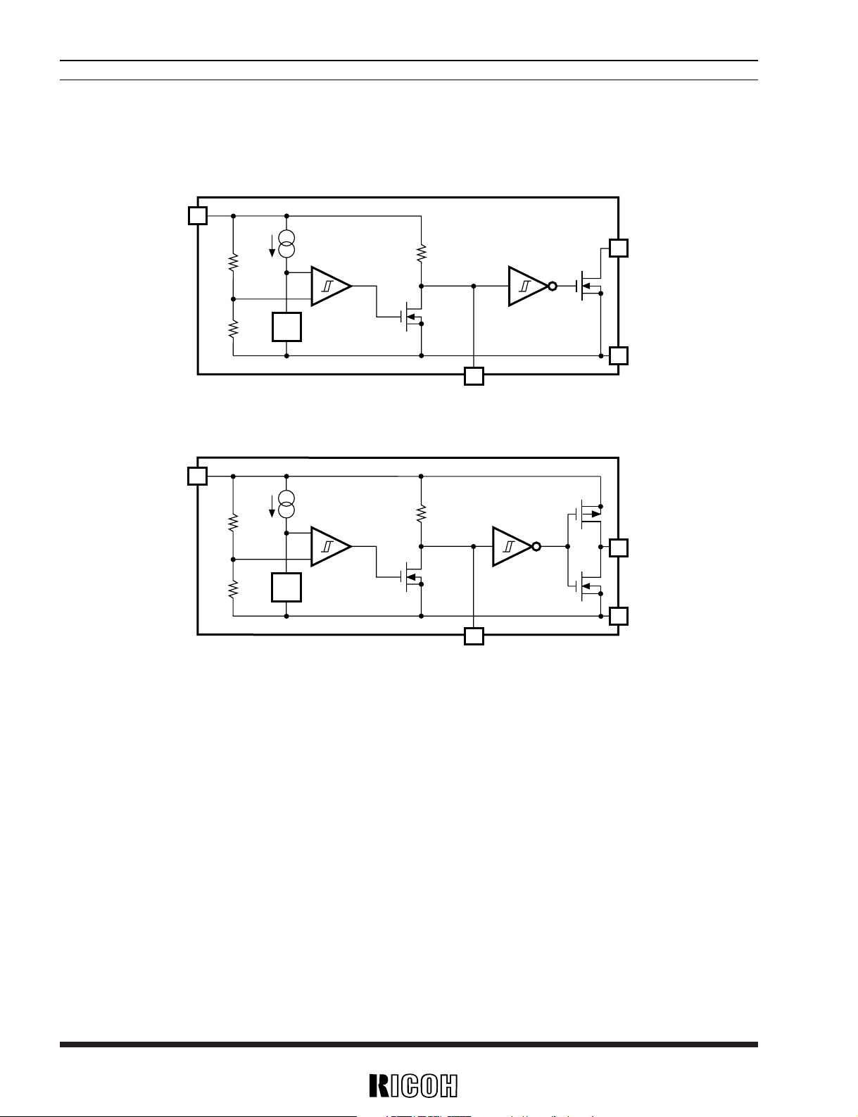
BLOCK DIAGRAMS
2
3
Vref
OUT
GND
V
DD
CD
RD
–
+
1
5
2
3
Vref
OUT
GND
V
DD
CD
RD
–
+
1
5
• Nch Open Drain Output (RN5VD××A)
• CMOS Output (RN5VD××C)
RN5VD××××
–
×× ← Part Number
↑↑↑ ↑
abc d
SELECTION GUIDE
The detector threshold, the output type, the packing type, and the taping type of RN5VD Series can be desig-
nating at the user's request by specifying the part number as follows :
For example, the Product with Detector Threshold 3.5V, Output Type Nch Open Drain and Taping Type TR,
is designated by Part Number RN5VD35AA-TR.
Code
a
Setting Detector Threshold (–V
DET
) :
Stepwise setting with a step of 0.1V in the range of 0.9V to 6.0V is possible.
b
Designation of Output Type
A: Nch Open Drain
C: CMOS
c
Designation of Packing Type
A: Taping
C: Antistatic bag for samples
d
Designation of Taping Type:
Ex. SOT-23-5: TR, TL
(refer to Taping Specification)
“TR” is prescribed as a standard.
Contents
RN5VD
3
}
}
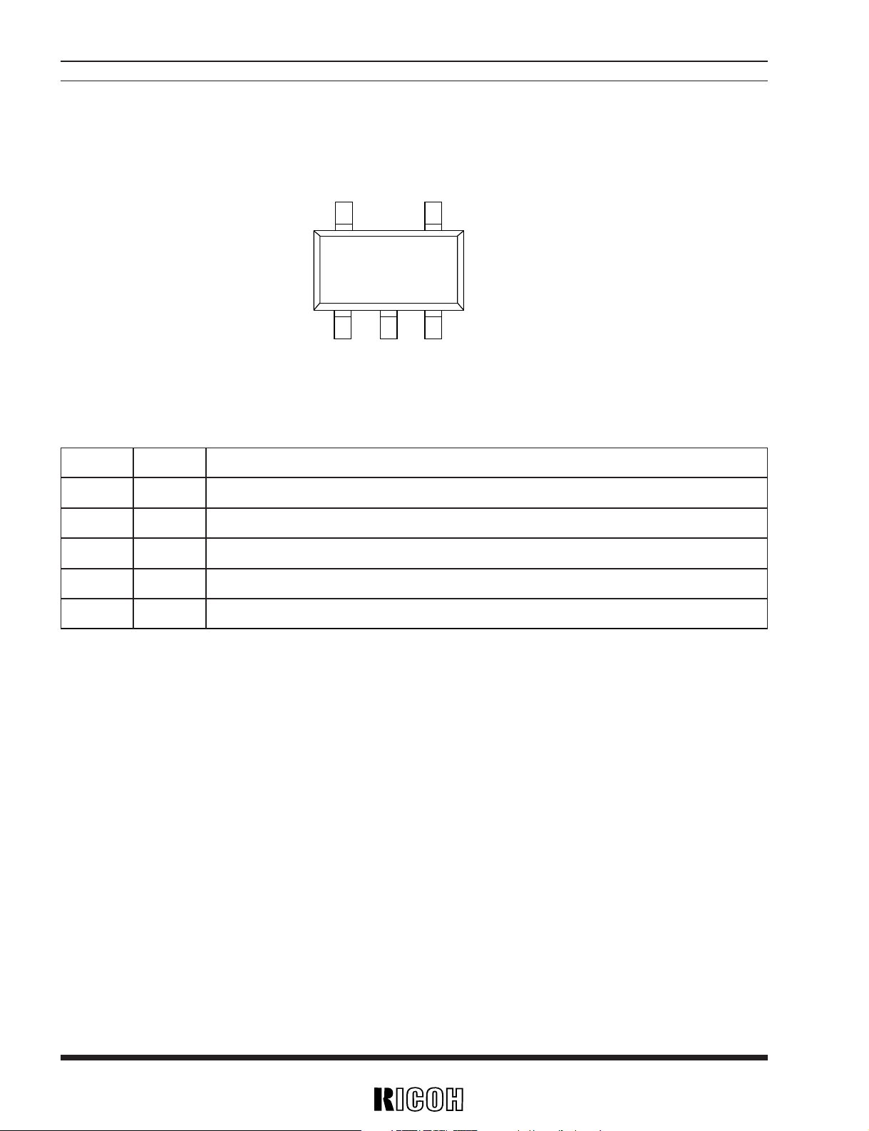
PIN DESCRIPTION
Pin No. Symbol Description
1 OUT Output Pin
Input and power source for device itself
Ground Pin
No Connection
Pin for external capacitor (for setting output delay)
2 V
DD
3 GND
4
NC
5 CD
RN5VD
4
PIN CONFIGURATION
• SOT-23-5
12
3
54
(mark side)
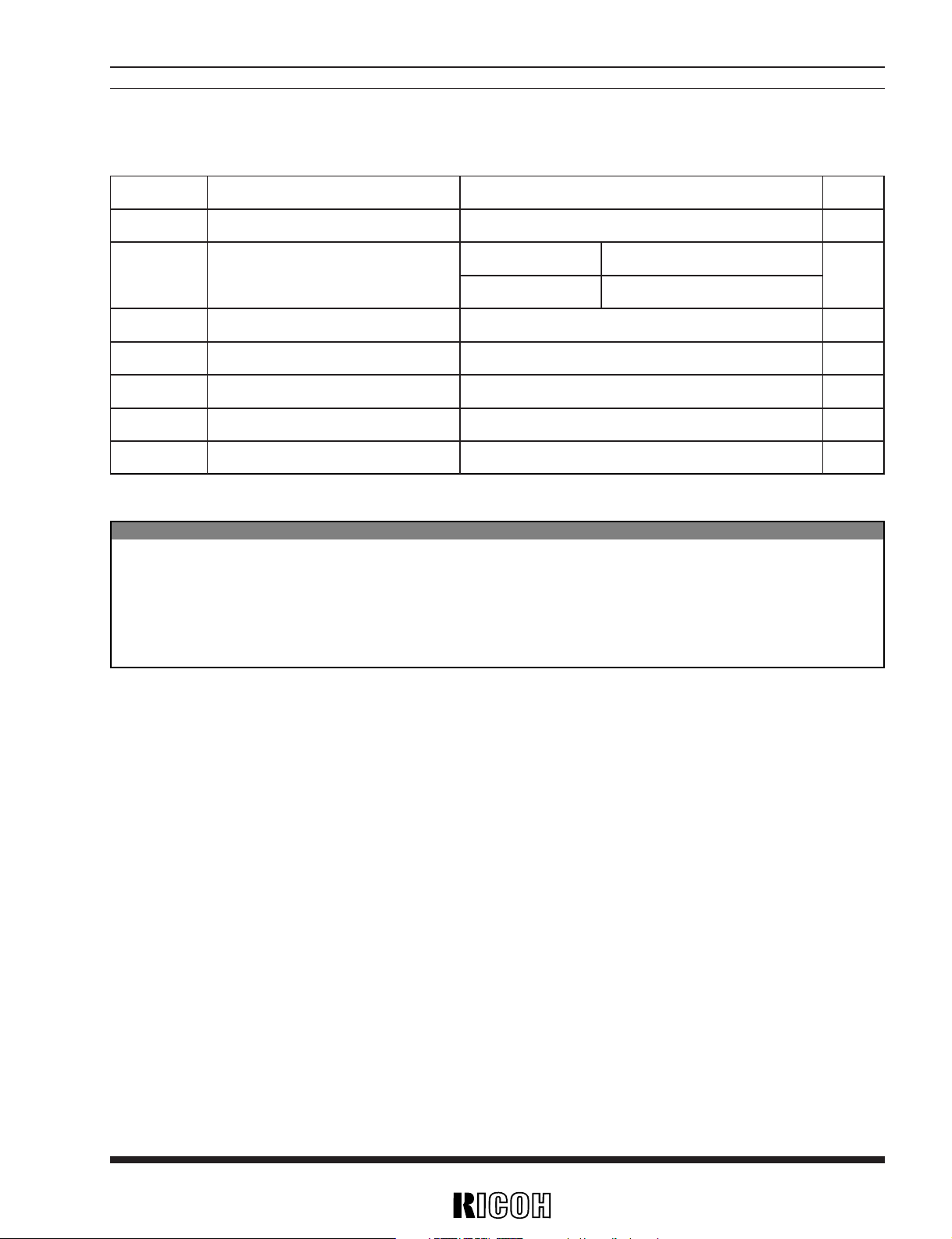
ABSOLUTE MAXIMUM RATINGS
Symbol Item Rating Unit
V
DD
Supply Voltage
12
V
OUT
Output Voltage
I
OUT
Output Current
Power Dissipation
CNOS VSS–0.3 to VDD+0.3
Nch
70
P
D
150
VSS–0.3 to 12
V
V
mA
mW
Operating Temperature Range
Topt
–40 to +85 ˚C
Storage Temperature RangeTstg –55 to +125 ˚C
Lead Temperature (Soldering) Tsolder 260˚C, 10s
Absolute Maximum ratings are threshold limit values that must not be exceeded even for an instant under any
conditions. Moreover, such values for any two items must not be reached simultaneously. Operation above
these absolute maximum ratings may cause degradation or permanent damage to the device. These are stress
ratings only and do not necessarily imply functional operation below these limits.
ABSOLUTE MAXIMUM RATINGS
RN5VD
5
RN5VD
6
VDD=0.8V
V
DD=2.9V
∆–VDET
∆Topt
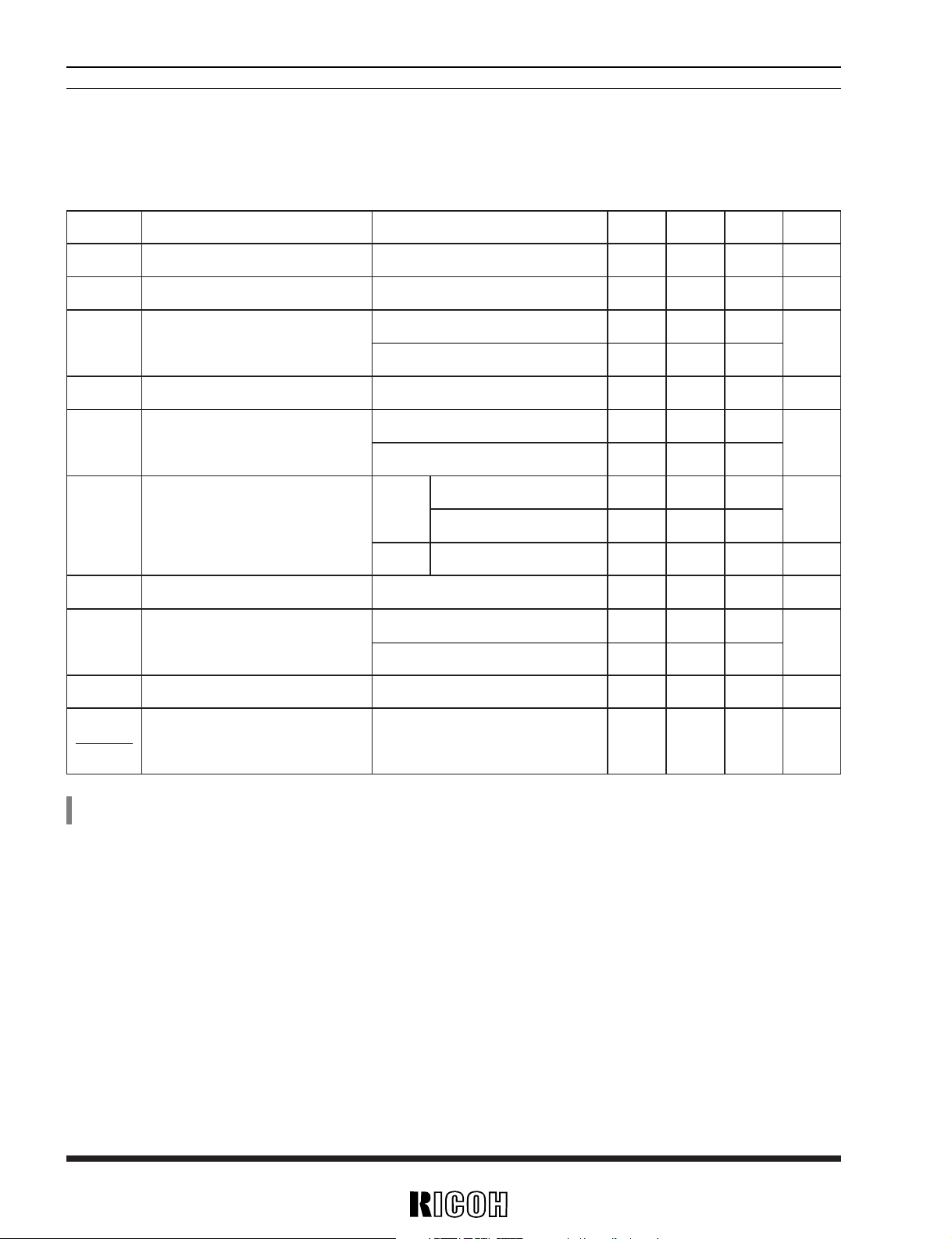
ELECTRICAL CHARACTERISTICS
• RN5VD09A/C
Topt=25˚C
Symbol Item Conditions MIN. TYP. MAX. Unit.
–VDET
VHYS
ISS
Detector Threshold
Detector Threshold Hysteresis
Supply Current
0.878 0.900 0.922 V
0.027 0.045 0.063 V
1.5
0.9
3.7
2.7
µA
VDDH Maximum Operating Voltage 10 V
VDDL
Minimum Operating Voltage
(
Note
1)
Topt=25˚C
–30˚C≤Topt≤85˚C
0.55
0.65
0.70
0.80
V
IOUT Output Current
Nch
Pch
VDS=0.05V, VDD=0.7V
VDS=0.5V, VDD=0.85V
VDS=–2.1V, VDD=4.5V
0.01
0.05
1.0
0.05
0.50
2.0
mA
VTCD CD pin Threshold Voltage VDD=0.99V 0.297 0.495 0.693 V
mA
RD Delay Resistance 0.5 1.0 2.0 MΩ
Detector Threshold
Temperature Coefficient
–30˚C≤Topt≤85˚C ±100 ppm/˚C
ICD CD pin Sink Current
VDS=0.1V, VDD=0.7V
V
DS=0.5V, VDD=0.85V
2.0
10.030100.0
µA
(Note 1) Minimum Operating Voltage means the value of input voltage when output voltage maintains 0.1V or less, provided that in the case of Nch
Open Drain Type Products, the pull-up resistance is set at 470kΩ, and the pull-up voltage is set at 5.0V.
RN5VD
7
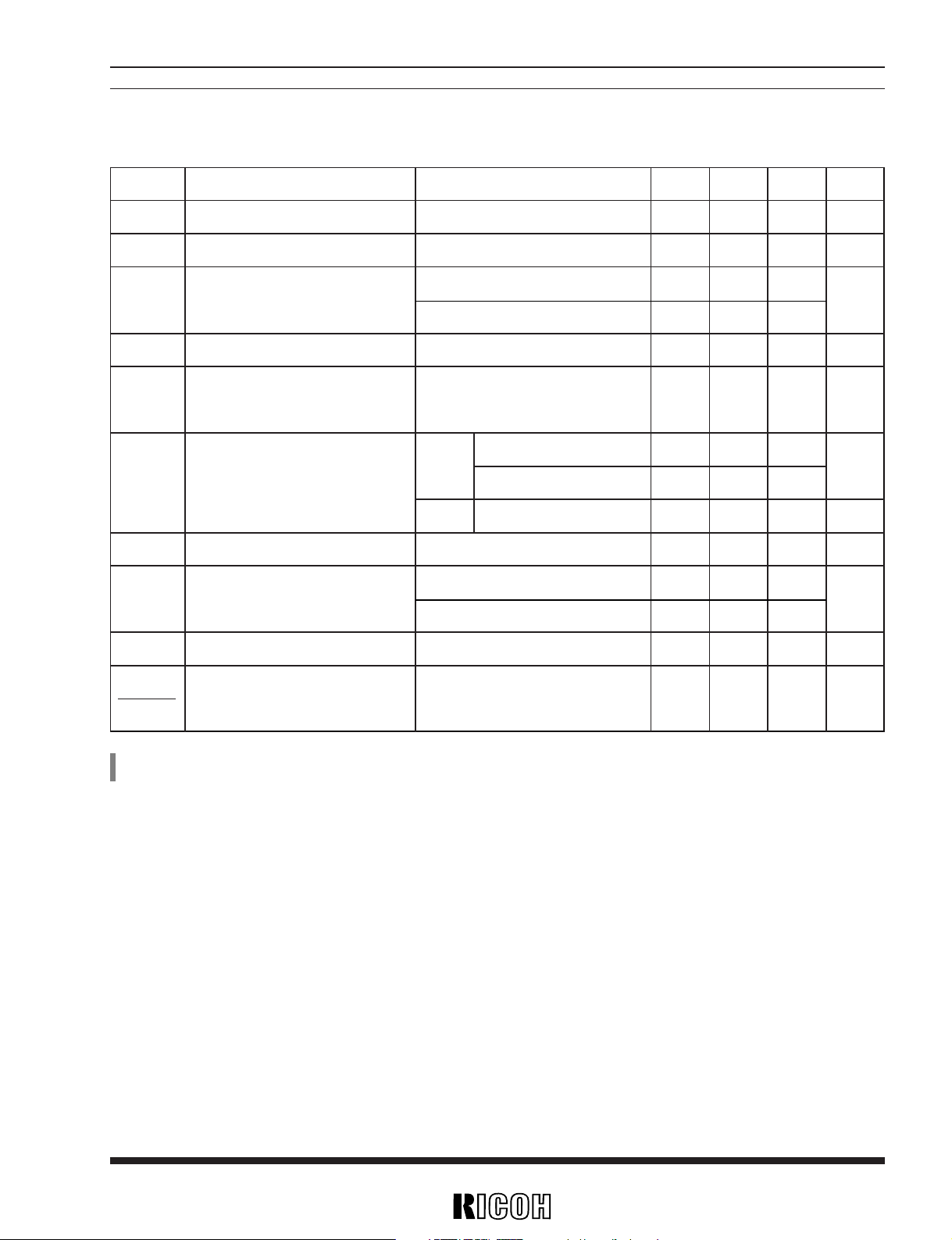
• RN5VD18A/C
Topt=25˚C
Symbol Item Conditions MIN. TYP. MAX. Unit.
–VDET
VHYS
ISS
VDDH
Detector Threshold
Detector Threshold Hysteresis
Supply Current
Maximum Operating Voltage
VDD=1.7V
V
DD=3.8V
1.755 1.800 1.845 V
0.054 0.090 0.126 V
2.5
1.0
5.0
3.0
µA
10 V
VDDL
Minimum Operating Voltage
(
Note
1)
Topt=25˚C
–30˚C≤Topt≤85˚C
0.55
0.65
0.70
0.80
V
IOUT Output Current
Nch
Pch VDS=–2.1V, VDD=4.5V
VDS=0.05V, VDD=0.7V
VDS=0.5V, VDD=1.5V
0.01
1.0
0.05
2.0
1.0 2.0
mA
mA
VTCD CD pin Threshold Voltage VDD=1.98V 0.693 0.990 1.287 V
ICD CD pin Sink Current
VDS=0.1V, VDD=0.7V
V
DS=0.5V, VDD=1.5V
2.0
200.030800.0
µA
RD Delay Resistance 0.5 1.0 2.0 MΩ
∆–V
DET
∆Topt
Detector Threshold
Temperature Coefficient
–30˚C≤Topt≤85˚C ±100 ppm/˚C
(Note 1) Minimum Operating Voltage means the value of input voltage when output voltage maintains 0.1V or less, provided that in the case of Nch
Open Drain Type Products, the pull-up resistance is set at 470kΩ, and the pull-up voltage is set at 5.0V.
RN5VD
8
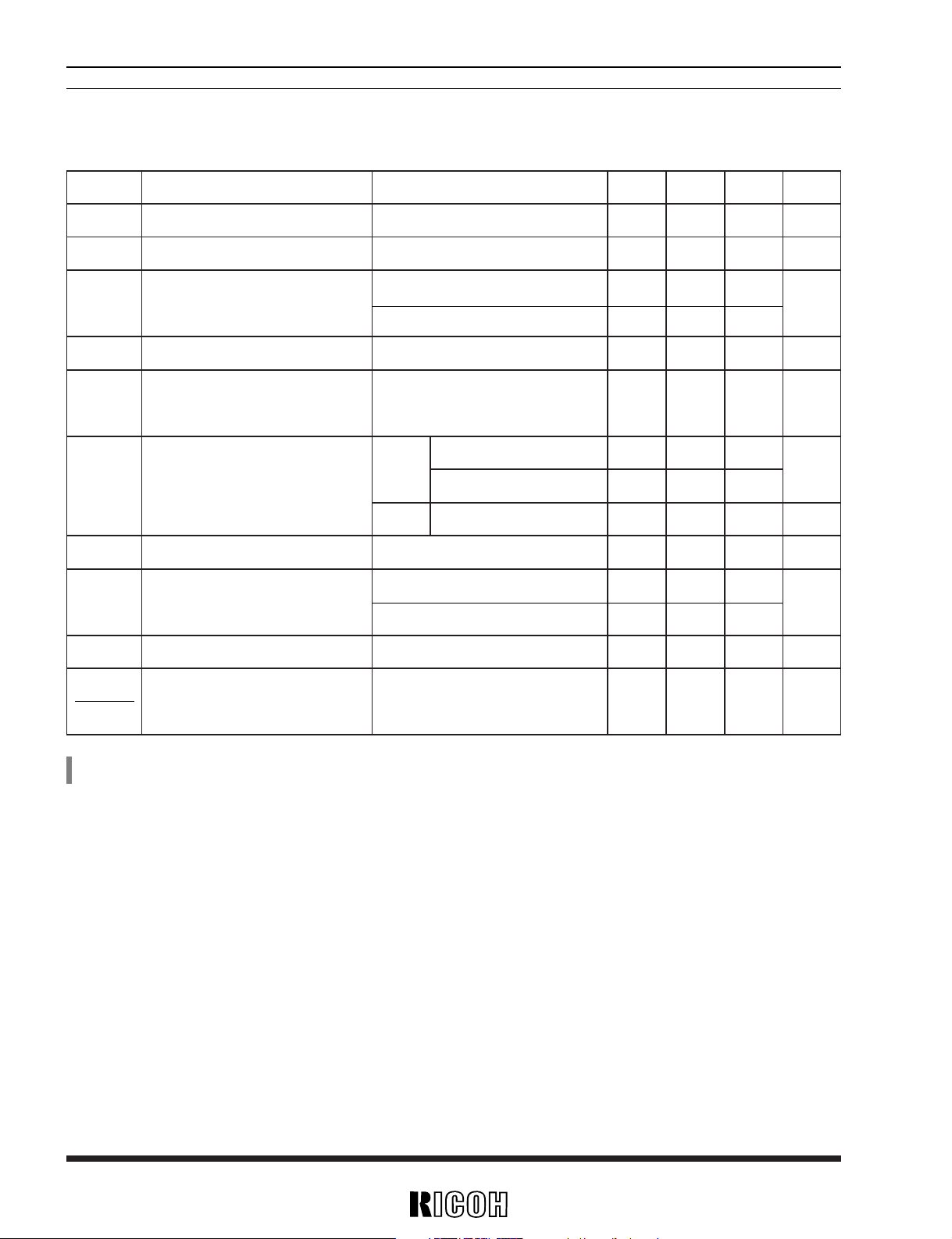
• RN5VD27A/C
Topt=25˚C
Symbol Item Conditions MIN. TYP. MAX. Unit.
–VDET
VHYS
ISS
VDDH
Detector Threshold
Detector Threshold Hysteresis
Supply Current
Maximum Operating Voltage
VDD=2.6V
V
DD=4.7V
2.633 2.700 2.767 V
0.081 0.135 0.189 V
3.5
1.1
7.0
3.3
µA
10 V
VDDL
Minimum Operating Voltage
(
Note
1)
Topt=25˚C
–30˚C≤Topt≤85˚C
0.55
0.65
0.70
0.80
V
IOUT Output Current
Nch
Pch VDS=–2.1V, VDD=4.5V
VDS=0.05V, VDD=0.7V
VDS=0.5V, VDD=1.5V
0.01
1.0
0.05
2.0
1.0 2.0
mA
mA
VTCD CD pin Threshold Voltage VDD=2.97V 1.188 1.485 1.782 V
ICD CD pin Sink Current
VDS=0.1V, VDD=0.7V
V
DS=0.5V, VDD=1.5V
2.0
200.030800.0
µA
RD Delay Resistance 0.5 1.0 2.0 MΩ
∆–VDET
∆Topt
Detector Threshold
Temperature Coefficient
–30˚C≤Topt≤85˚C ±100 ppm/˚C
( Note 1) Minimum Operating Voltage means the value of input voltage when output voltage maintains 0.1V or less, provided that in the case of Nch
Open Drain Type Products, the pull-up resistance is set at 470kΩ, and the pull-up voltage is set at 5.0V.
 Loading...