


Charge-Pump for White LED and Power Supply
RN5T652
Development Specifications
Rev. 1.5
2009.05.19
RICOH COMPANY, LTD.
Electronic Devices Company
This specification is subject to change without notice.
RN5T652 Rev.1.5
Table of Contents
1.
Outline ..................................................................................................................................................... 3
2. Feature ..................................................................................................................................................... 3
3. Pin Configuration ..................................................................................................................................... 4
4. Block Diagram.......................................................................................................................................... 5
5. Pin Description ......................................................................................................................................... 6
6. Functional Blocks ..................................................................................................................................... 7
6.1 Regulators.............................................................................................................................................. 7
6.1.1 LDO1 Electrical Characteristics ................................................................................................................ 7
6.1.2 LDO2 Electrical Characteristics ................................................................................................................ 8
6.2 Thermal Shutdown Circuit....................................................................................................................... 9
6.2.1 Thermal Shutdown Block Diagram ........................................................................................................... 9
6.2.2 Thermal Shutdown Explanation of Operation...........................................................................................9
6.2.3 Thermal Shutdown Electrical Characteristics............................................................................................ 9
6.3 Charge Pump........................................................................................................................................ 10
6.3.1 Block Diagram......................................................................................................................................... 10
6.3.2 Operation ................................................................................................................................................. 11
6.3.3 Protection Circuit..................................................................................................................................... 12
6.3.4 Unused DIN_ Pin..................................................................................................................................... 12
6.3.5 Soft-start .................................................................................................................................................. 12
6.3.6 Charge Pump Electrical Characteristics................................................................................................... 13
6.3.7 STBB Logic Input ................................................................................................................................... 14
6.4 UVLO (Under Voltage Lock Out).......................................................................................................... 14
6.5 CPU Interface....................................................................................................................................... 15
6.5.1 Start and Stop Condition.......................................................................................................................... 15
6.5.2 Data Transmission and its Acknowledge................................................................................................. 16
6.5.3 I2C -Bus Slave Address........................................................................................................................... 16
6.5.4 Data Transmission Write Format............................................................................................................. 17
6.5.5 Internal Register Write-in Timing ........................................................................................................... 17
6.5.6 Connection of I2C-Bus............................................................................................................................ 18
6.5.7 AC Characteristics of I2C-Bus ................................................................................................................ 19
7. Register .................................................................................................................................................. 20
7.1 Register Map........................................................................................................................................ 20
7.2 Main / Sub / Flash / Strobe Luminance ................................................................................................... 21
Page 1 ©2009 Rev. 1.5

RN5T652 Rev.1.5
7.3 LDO1 / LDO2 Output Voltage ............................................................................................................... 22
7.4 Others Function.................................................................................................................................... 22
8. Electrical Characteristics........................................................................................................................ 23
8.1 Absolute Maximum Ratings .................................................................................................................. 23
8.2 Recommendation of Operation Conditions.............................................................................................. 23
8.3 General Characteristics.......................................................................................................................... 23
8.4 DC Characteristics ................................................................................................................................24
9. Additional Application Circuit................................................................................................................ 25
10. Package Information .............................................................................................................................. 27
©2009 Rev. 1.5
Page 2
RN5T652 Rev. 1.5
1. Outline
RN5T652 contains constant frequency charge pump to optimize for white LED application and two low-noise LDOs.
Output enable/disable, LEDs current setting and LDO output voltage setting are individually controllable through I2C.
2. Feature
z Power Supply Function
9 LDO × 2 (ON/OFF programmable)
9 Over current Protection (All Regulators) and thermal shutdown
z White LED Charge Pump
9 Current capability: All currents capability 450mA
9 Flash at 300mA max.
9 Four Main LEDs at 25mA max.
9 Two Sub LEDs 25mA max.
z I2C-Bus (Max: 400kHz)
9 Address = 64h
9 ON/OFF control
9 Individual LEDs current value setting
9 Individual LDOs voltage value setting
z Others
9 Soft-start circuit
9 Short-circuit protection, open-circuit and thermal protection
z Package
9 28pin thin QFN package (Body size: 4 x 4 x 0.8mm)
z Process
9 CMOS process
©2009 Rev. 1.5 Page 3
RN5T652 Rev. 1.5
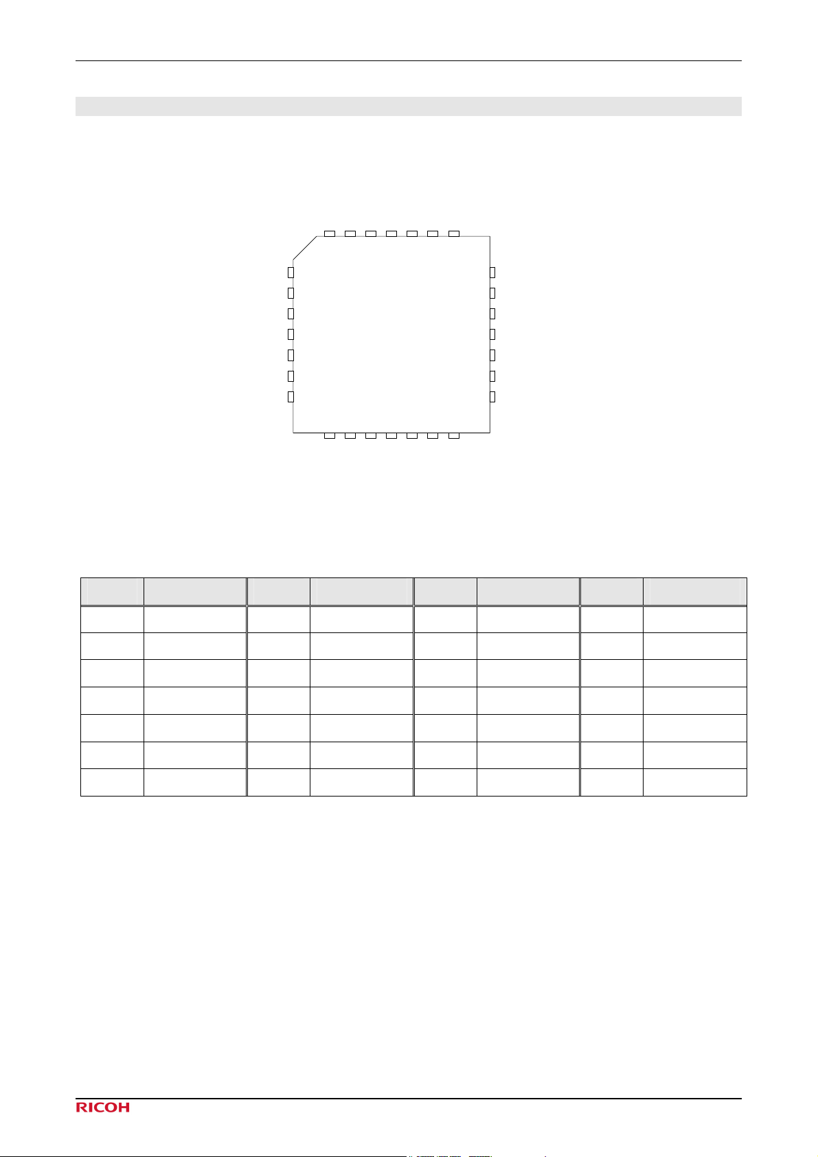
3. Pin Configuration
(TOP VIEW)
DIN3
DIN2
DIN1
VOUT
C1P
C2P
C2M
GND1
DIN5
DIN4
28
27
26
DIN6
25
1
2
3
4
RN5T652
5
6
7
10
C1M
VIN1
11
VEN
9
8
PGND1
DIN7
24
12
STBB
GND2
23
13
SCL
VREF
22
14
SDA
LDOUT1
21
VIN3
20
LDOUT2
19
N.C.
18
N.C.
17
N.C.
16
N.C.
15
QFN0404-28 pin
Pin No. Name Pin No. Name Pin No. Name Pin No. Name
1 DIN3 8 PGND1 15 N.C. 22 VREF
2 DIN2 9 C1M 16 N.C. 23 GND2
3 DIN1 10 VIN1 17 N.C. 24 DIN7
4 VOUT 11 VEN 18 N.C. 25 DIN6
5 C1P 12 STBB 19 LDOUT2 26 DIN5
6 C2P 13 SCL 20 VIN3 27 GND1
7 C2M 14 SDA 21 LDOUT1 28 DIN4
Fig 3-1 Pin Configuration
©2009 Rev. 1.5 Page 4
RN5T652 Rev. 1.5
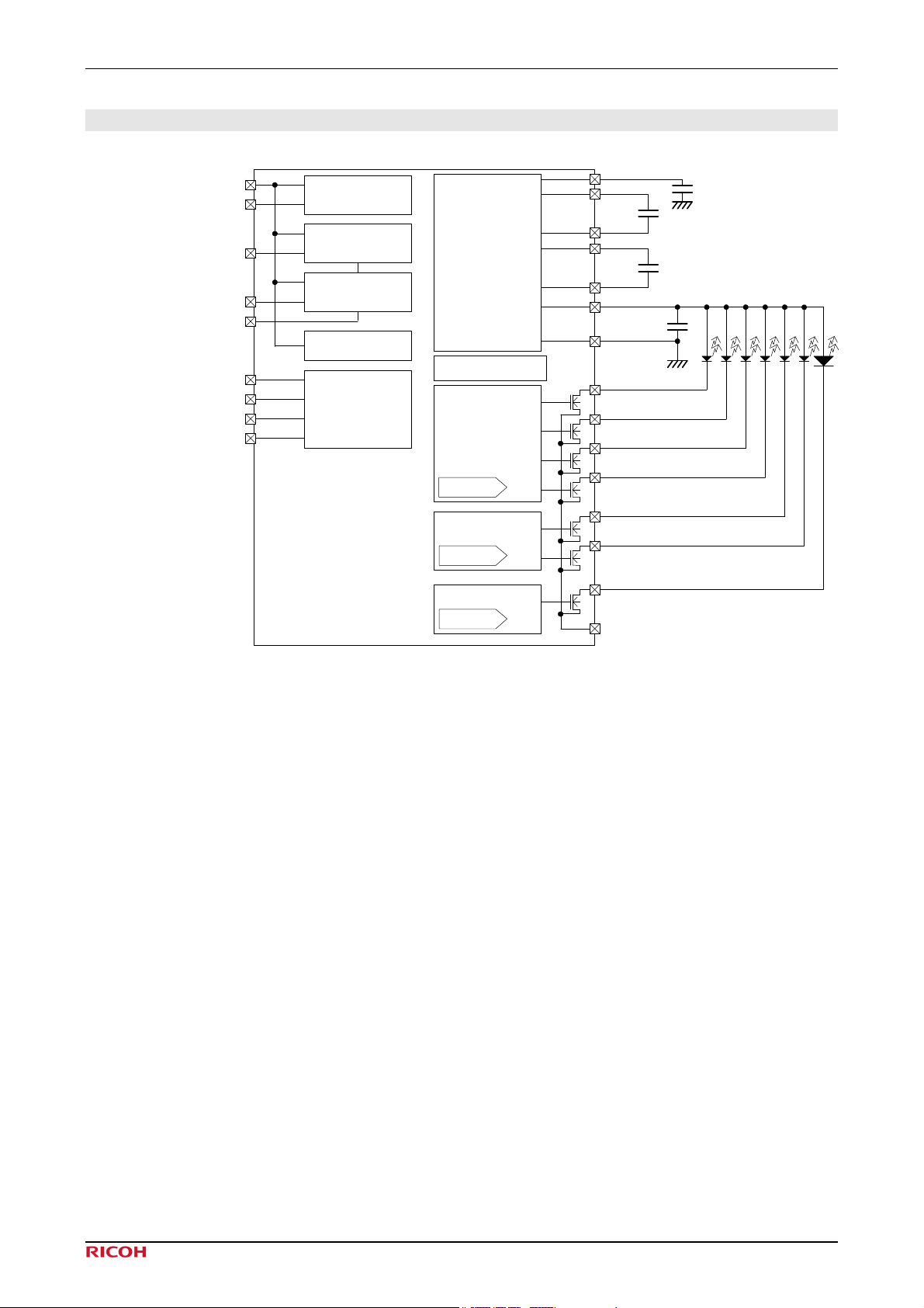
4. Block Diagram
VIN3
VREF
LDOUT1
LDOUT2
GND2
VEN
SCL
SDA
STBB
VREF
LDO1
LDO2
UVLO
Digital
Charge Pump
@450mA
Thermal
Shutdown
CC Driver
(Main)
5bit DAC
CC Driver (Sub)
5bit DAC
VIN1
C2P
1uF
C2M
C1P
1uF
C1M
VOUT
2.2uF
PGND1
DIN1
@25mA
DIN2
@25mA
DIN3
@25mA
DIN4
@25mA
DIN5
@25mA
DIN6
@25mA
4.7uF
GND
GND
CC Driver (Flash)
5bit DAC
Fig 4-1 Block Diagram
DIN7
@300mA
GND1
©2009 Rev. 1.5 Page 5
RN5T652 Rev. 1.5
5. Pin Description
No. Name I/O
1 DIN3 O LED driver current control output 3
2 DIN2 O LED driver current control output 2
3 DIN1 O LED driver current control output 1
4 VOUT O LED driver voltage output
5 C1P - Charge pump boost capacitor connection
6 C2P - Charge pump boost capacitor connection
7 C2M - Charge pump boost capacitor connection
8 PGND1 - Ground (charge pump)
9 C1M - Charge pump boost capacitor connection
10 VIN1 - Power supply (charge pump)
11 VEN - Voltage supply (I2C), enable input
12 STBB I Strobe enable input
13 SCL I I2C interface clock input
14 SDA I/O I2C interface data input
15 N.C. - Non-connect
16 N.C. - Non-connect
17 N.C. - Non-connect
18 N.C. - Non-connect
19 LDOUT2 O LDO2 output
20 VIN3 - Power supply
21 LDOUT1 O LDO1 output
22 VREF O Bypass capacitor connecting pin
23 GND2 - Ground
24 DIN7 O LED driver current control output 7
25 DIN6 O LED driver current control output 6
26 DIN5 O LED driver current control output 5
27 GND1 - Ground
28 DIN4 O LED driver current control output 4
Function Notes
Table 5-1 Pin Description
©2009 Rev. 1.5 Page 6
RN5T652 Rev. 1.5
6. Functional Blocks
6.1 Regulators
6.1.1 LDO1 Electrical Characteristics
Operating Conditions (Unless otherwise specified) V
BATT
= 3.6V, C
= 1μF, Ta = 25℃
REFO
Symbol Parameter Condition Min Typ Max Units
VOUT1 Output Voltage
50μA<IOUT1<300mA
VOUT1+0.5V≦V
BATT
(VIN)≦4.5V
-2% 1.50 +2% V
IOUT1 Output Current - 300 mA
ILIM1 Current Limit VOUT1=1.5V 500 mA
VDRP1 Drop-out Voltage IOUT1=200mA, Ta =85℃ 200 mV
ΔVOUT1
ΔVIN
ΔVOUT1
ΔIOUT1
ΔVOUT1
ΔT
a
Line Regulation
Load Regulation 50μA<IOUT1<300mA 25 mV
Output Voltage
Temperature
Coefficient
RR1 Ripple Rejection
EN1
Output Noise
(RMS)
VOUT1+0.5V≦V
BATT
IOUT1=150mA
-40℃≦T
≦85℃ +100 ppm/℃
a
f=10Hz-10kHz, C
IOUT1=30mA
BW=100Hz-100kHz, C
IOUT1=30mA
(VIN)≦4.5V
=2.2μF
out
=2.2μF
out
2.4 mV
60 dB
35 μVrms
BC1 Bypass Capacitor 0μA<IOUT1<300mA 2.2 μF
ISS1 Supply Current
Normal (IOUT1=Max) 50*1
OFF 1
μA
1.50
1.80
2.50
2.60
2.80
3.00
3.10
3.30
1.85 *
+2% V
POUT1
Programmable
Output Voltage
IOUT1=300mA -2%
2.40 *
2.55 *
2.70 *
2.85 *
2.90 *
3.20 *
Table 6-1 LDO1 Electrical Characteristics
Note*: Bypass capacitor: 2.2μF, in mounted state.
For optimized phase compensation, the bypass capacitor must be the ceramic type.
©2009 Rev. 1.5 Page 7
RN5T652 Rev. 1.5
6.1.2 LDO2 Electrical Characteristics
Operating Conditions (Unless otherwise specified) VBATT = 3.6V, CREFO = 1μF, Ta = 25℃
Symbol Parameter Condition Min Typ Max Units
VOUT2 Output Voltage
50μA<IOUT2<300mA
VOUT2+0.5V≦V
BATT
(VIN)≦4.5V
-2% 1.50 +2% V
IOUT21 Output Current - 300 mA
ILIM2 Current Limit VOUT2=1.5V 500 mA
VDRP2 Drop-out Voltage IOUT2=200mA, Ta =85℃ 200 mV
ΔVOUT2
ΔVIN
ΔVOUT2
ΔIOUT2
ΔVOUT2
ΔT
a
Line Regulation
Load Regulation 50μA<IOUT2<300mA 25 mV
Output Voltage
Temperature
Coefficient
RR2 Ripple Rejection
EN2
Output Noise
(RMS)
VOUT2+0.5V≦V
BATT
IOUT2=150mA
-40℃≦T
≦85℃ +100 ppm/℃
a
f=10Hz-10kHz, C
IOUT2=30mA
BW=100Hz-100kHz, C
IOUT2=30mA
(VIN)≦4.5V
=2.2μF
out
=2.2μF
out
2.4 mV
60 dB
35 μVrms
BC2 Bypass Capacitor 0μA<IOUT2<300mA 2.2 μF
ISS2 Supply Current
Normal (IOUT2=Max) 50*1
μA
OFF 1
1.50
1.80
2.50
2.60
2.80
3.00
3.10
3.30
1.85 *
+2% V
POUT2
Programmable
Output Voltage
IOUT2=300mA -2%
2.40 *
2.55 *
2.70 *
2.85 *
2.90 *
3.20 *
Table 6-2 LDO2 Electrical Characteristics
Note*: Bypass capacitor: 2.2μF, in mounted state.
For optimized phase compensation, the bypass capacitor must be the ceramic type.
Note*1: Vref Block Supply Current typ 20μA
ex)LDO1+LDO2+Vref =120μA(typ)
LDO1+Vref=70μA(typ)
©2009 Rev. 1.5 Page 8
 Loading...