


RN5T614 POWER MANAGEMENT SYSTEM DEVICE
POWER MANAGEMENT SYSTEM DEVICE
RN5T614x
Product Specifications
Rev. 1.0
2011.10.06
RICOH COMPANY, LTD.
Electronic Devices Company
This specification is subject to change without notice.
©2010-2011 Rev. 1.0 Page 1

RN5T614 POWER MANAGEMENT SYSTEM DEVICE
Table of Contents
1. Outline......................................................................................................................................................................... 4
2. Feature......................................................................................................................................................................... 4
3. Pin Configuration ........................................................................................................................................................6
4. Block Diagram ............................................................................................................................................................7
5. Pin Description............................................................................................................................................................8
6. Power Control ...........................................................................................................................................................10
6.1 Power Control Block Diagram..........................................................................................................................10
6.2 Power on and off...............................................................................................................................................11
6.3 Soft Reset Operation.........................................................................................................................................13
6.4 Stand-by Operation ...........................................................................................................................................14
6.5 UVLO (Under Voltage Lock Out) Electrical Characteristics ........................................................................... 15
6.6 TSHUT (Thermal Shutdown Circuit) Electrical Characteristics.......................................................................15
7. Voltage Detector .......................................................................................................................................................16
7.1 VBAT Detector (VD1) Electrical Characteristics.............................................................................................16
7.2 RESDET Detector (VD2) Electrical Characteristics.........................................................................................16
8. Regulator ...................................................................................................................................................................17
8.1 Regulator Table.................................................................................................................................................17
8.2 Step-down DC/DC Converter ...........................................................................................................................18
8.3 LDO ..................................................................................................................................................................22
9. Li-ion Battery Charger ..............................................................................................................................................26
9.1 Li-ion Battery Charger Block Diagram.............................................................................................................26
9.2 Explanation of Charge Block Operating ...........................................................................................................27
9.3 Charge Interrupt Request ..................................................................................................................................32
9.4 Li-ion Battery Charger Electrical Characteristics .............................................................................................33
10. Interrupt Controller (INTC).......................................................................................................................................35
10.1 Interrupt Controller Block Diagram..................................................................................................................35
10.2 Interrupt Timing Chart......................................................................................................................................36
10.3 Interrupt Request List........................................................................................................................................37
11. CPU Interface............................................................................................................................................................38
11.1 I2C-Bus Operation............................................................................................................................................38
11.2 I2C-Bus Data Transmission and its Acknowledge............................................................................................39
11.3 I2C-Bus Slave Address .....................................................................................................................................39
©2010-2011 Rev. 1.0 Page 2

RN5T614 POWER MANAGEMENT SYSTEM DEVICE
11.4 I2C-Bus Data Transmission Read Format ........................................................................................................40
11.5 I2C-Bus Data Transmission Write Format........................................................................................................40
11.6 I2C-Bus Internal Register Write-in Timing ......................................................................................................41
11.7 AC Characteristics of I2C-Bus..........................................................................................................................42
12. Registers....................................................................................................................................................................43
12.1 Power Control ...................................................................................................................................................44
12.2 Voltage Detector ...............................................................................................................................................45
12.3 Regulator...........................................................................................................................................................46
12.4 Li-ion Battery Charger......................................................................................................................................55
12.5 Interrupt Controller ...........................................................................................................................................60
13. Electrical Characteristics...........................................................................................................................................65
13.1 Absolute Maximum Ratings .............................................................................................................................65
13.2 Recommendation of Operating Conditions.......................................................................................................65
13.3 DC Characteristics ............................................................................................................................................66
14. Appendix...................................................................................................................................................................67
©2010-2011 Rev. 1.0 Page 3

RN5T614 POWER MANAGEMENT SYSTEM DEVICE
1. Outline
RN5T614 is the power management IC for GPS-PND/MID and Smart-Phone.
It integrates three high-efficiency step-down DCDC controllers, eight low dropout regulators, power control logic,
Li-ion Battery Charger, I2C-Bus Interface, voltage detections, thermal shut-down, UVLO and etc.
2. Feature
●System
9 Thermal Shutdown Function
9 Reset Detector Function
9 UVLO Function
9 I2C-Bus Interface @400kHz (Input voltage range: 1.7V-3.4V)
●High Efficiency Step-down DC/DC Converters
9 DC/DC1: 1.20V (0.9V to 1.5V/12.5mV steps) @1200mA with RAMP control (For Core)
9 DC/DC2: 1.15V (0.9V to 1.5V/12.5mV steps and 1.8V) @1000mA with RAMP control (For Logic)
9 DC/DC3: 1.8V (1.8V to 3.3V by external resistors) @500mA (For Memory)
9 DC/DC on/off control pin for DC/DC1 and DC/DC2
●Low Drop Voltage Regulators
9 LDO1:3.0V (Always-on) @10mA
9 LDO2:1.2V (0.9V/1.0V/1.1V/1.2V/1.3V) @30mA
9 LDO3:1.2V (0.9V/1.0V/1.1V/1.2V/1.3V) @30mA
9 LDO4:3.3V (1.8V/2.5V/2.6V/2.8V/2.85V/3.0V/3.3V) @300mA
9 LDO5:1.8V (1.8V/2.5V/2.6V/2.8V/2.85V/3.0V/3.3V) @300mA
9 LDO6:2.6V (1.2V/1.8V/2.5V/2.6V/2.8V/2.85V/3.0V/3.3V) @150mA
9 LDO7:3.0V (1.2V/1.8V/2.5V/2.6V/2.8V/2.85V/3.0V/3.3V) @150mA
9 LDO8:3.3V (1.8V/2.5V/2.6V/2.8V/2.85V/3.0V/3.3V) @150mA
●Li-ion Battery Charger
9 Support AC adapter charging
9 With the current limit protection and charge current control, the limited power can be efficiently
supplied to the system and the battery.
9 The system can power on even when Li-ion Battery is low voltage or open.
9 The device can withstand up to 6.5V on VCHG pin. However, it can withstand high voltage by
combining a high voltage protection IC (up to 28V by using BD6040 of ROHM).
9 Rapid timer and Trickle timer integrated.
9 Monitor for the battery thermistor built in.
9 No external MOSFET required.
9 If system loads over AC adapter current rating, the battery will supply the current to the system.
9 Chip temperature detection circuit for over temperature protection integrated.
●Package QFN0606-48
●Process CMOS
©2010-2011 Rev. 1.0 Page 4
y
RN5T614 POWER MANAGEMENT SYSTEM DEVICE
◎Version List
Version No DC/DC Preset LDO Setting
LDO1: 3.0V
LDO2: Power-on
RN5T614A
RN5T614B
RN5T614C
RN5T614D
RN5T614E
RN5T614F
Note*: For the trimming of regulators, refer to Chapter 8.1 Regulator Table.
DC/DC1: 1.25V
DC/DC2: 1.20V
DC/DC1: 1.25V
DC/DC2: 1.20V
DC/DC1: 1.20V
DC/DC2: 1.80V
DC/DC1: 1.20V
DC/DC2: 1.80V
DC/DC1: 1.20V
DC/DC2: 1.15V
DC/DC1: 1.25V
DC/DC2: 1.20V
LDO3-5: Initial On
LDO5: 3.0V
LDO8: 3.0V
VREF: Power-on
LDO1: 3.0V
LDO2: Power-on
LDO3-5: Initial On
LDO5: 3.0V
LDO8: 3.0V
VREF: Power-on
LDO1: 3.0V
LDO2: Power-on
LDO3-5: Initial On
LDO5: 1.8V
LDO8: 3.3V
VREF: Power-on
LDO1: 1.8V
LDO2: Always-on
LDO3-5: Initial Off
LDO5: 1.8V
LDO8: 3.3V
VREF: Alwa
LDO1: 3.0V
LDO2: Power-on
LDO3-5: Initial On
LDO5: 1.8V
LDO8: 3.3V
VREF: Power-on
LDO1: 3.0V
LDO2: Power-on
LDO3-5: Initial On
LDO5: 3.0V
LDO8: 3.3V
VREF: Power-on
DCDCEN*
Valid Condition
DCDCEN12 :
2ms after the start of power-on
DCDCEN3 :
Invalid by trimming
DCDCEN12 :
After RESETO is released
DCDCEN3 :
Invalid by trimming
DCDCEN12 :
After RESETO is released
DCDCEN3 :
Invalid by trimming
DCDCEN12 :
After RESETO is released
DCDCEN3 :
After RESETO is released
s-on
DCDCEN12 :
After RESETO is released
DCDCEN3 :
Invalid by trimming
DCDCEN12 :
After RESETO is released
DCDCEN3 :
Invalid by trimming
For the detail of Sequence, refer to Appendix.
Sequence
Sequence1
Sequence2
Sequence2
Sequence4
Sequence2
Sequence3
The initial value of the following pages is based on RN5T614E!!
©2010-2011 Rev. 1.0 Page 5
RN5T614 POWER MANAGEMENT SYSTEM DEVICE
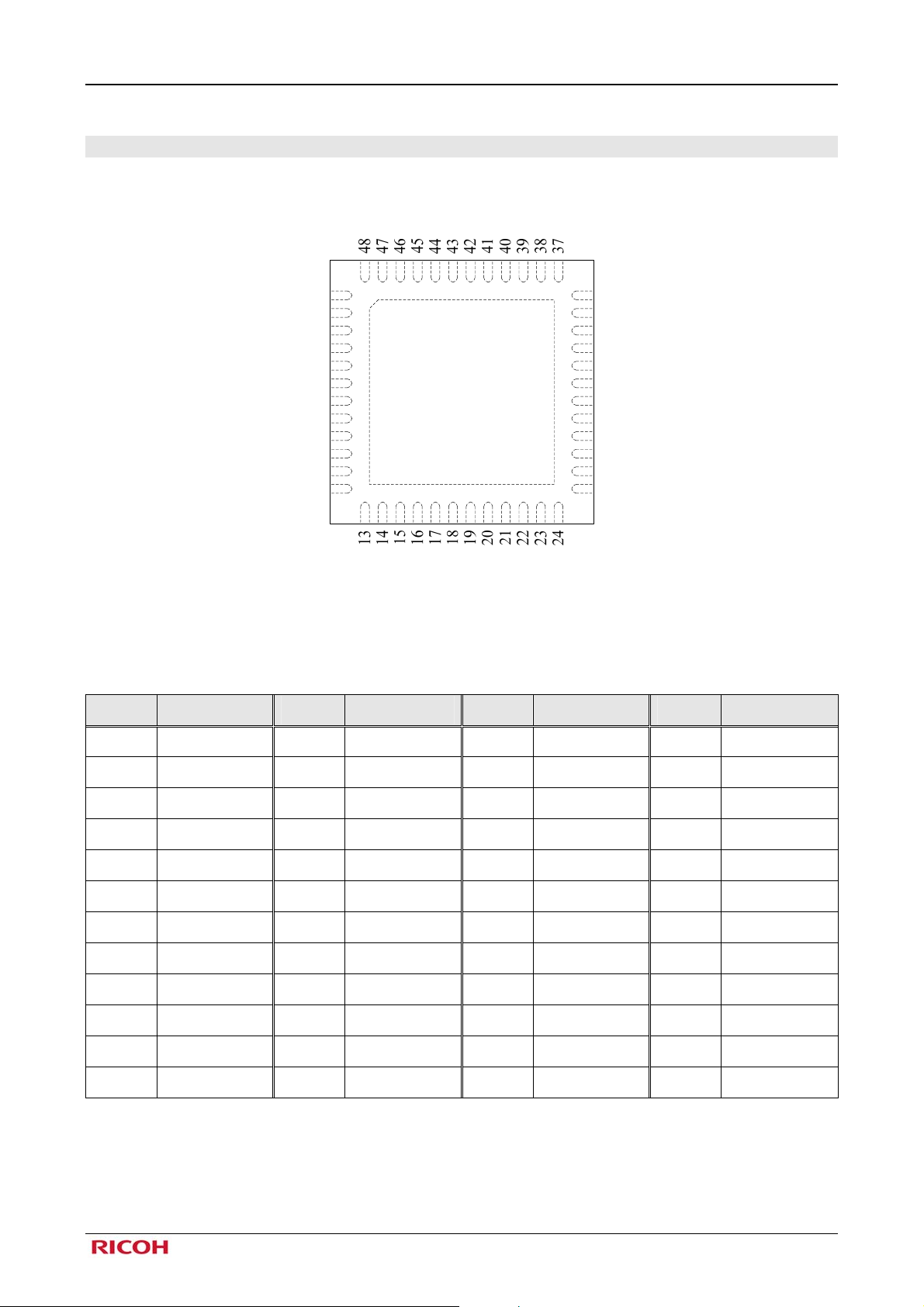
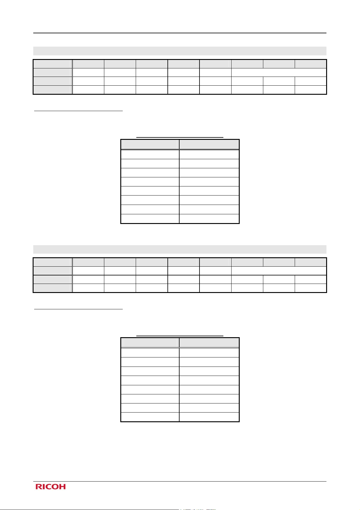
3. Pin Configuration
1
2
3
4
5
6
7
8
9
10
11
12
Fig 3-1 Package Information (QFN0606-48pin)
Pin No. Name Pin No. Name Pin No. Name Pin No. Name
1 VOUT5 13 TEST1 25 DCDCEN12 37 VSYS1
Top View
QFN0606-48
GND *1
36
35
34
33
32
31
30
29
28
27
26
25
2 VIN2 14 TEST2 26 INTB 38 VSYS2
3 VOUT6 15 VFB1 27 PSHOLD 39 VSYS3
4 VOUT7 16 LX1 28 VDDIO 40 VCHG
5 VIN3 17 VINP1 29 SDA 41 CHGLED
6 VOUT8 18 VINP2 30 SCL 42 VOUTD
7 VINA 19 LX2 31 THERMBAT 43 VREF
8 RESETO 20 VFB2 32 VTHM 44 VOUT3
9 BATDET 21 VINP3 33 VCHGREG 45 VOUT2
10 EXTON 22 LX3 34 IMONI 46 VIN1
11 PWRON 23 VFB3 35 VBAT1 47 VOUT4
12 ONOB 24 DCDCEN3 36 VBAT2 48 VOUT1
Note*1: Tab on the bottom side must be connected to GND.
©2010-2011 Rev. 1.0 Page 6
RN5T614 POWER MANAGEMENT SYSTEM DEVICE
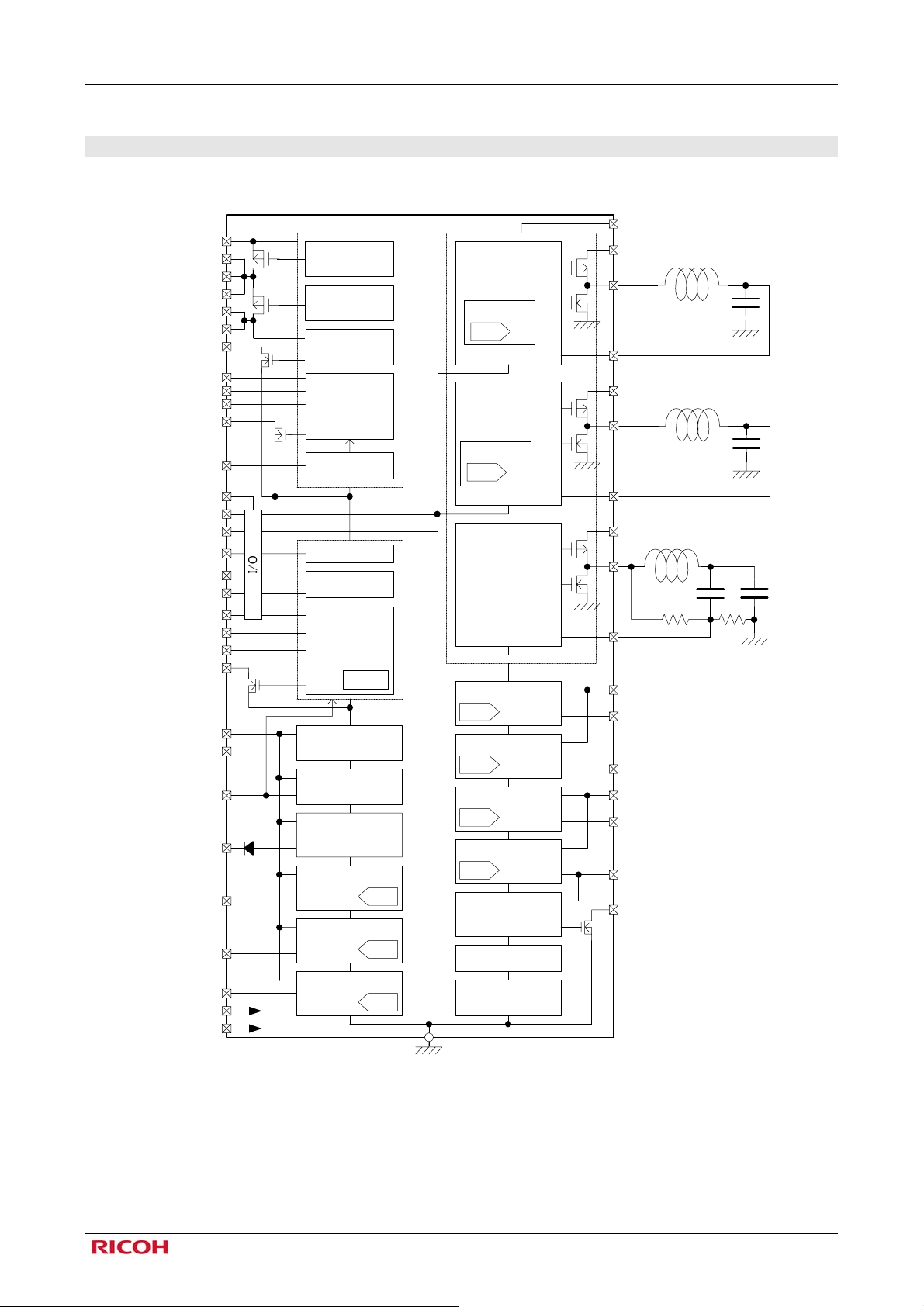
4. Block Diagram
VCHG
VSYS1
VSYS2
VSYS3
VBAT1
VBAT2
BATDET
THERMBAT
VTHM
IMONI
CHGLED
VCHGREG
VDDIO
DCDCEN12
DCDCEN3
INTB
SDA
SCL
PSHOLD
EXTON
PWRON
ONOB
VIN1
VREF
VOUTD
VOUT1
VOUT2
VOUT3
Li-ion Battery Charge
*1
Power Pass
Control
Li-ion Battery
Charger
VD1
Charge
Control logic
Charge REG
INTC
I2CIF
Power ON
Sequence
OSC
VREF
LDODIG
(for Internal Use)
(Always ON)
LDO1(10mA)
(Always ON)
LDO2(30mA)
DAC
LDO3(30mA)
DAC
DC/DC1
for Core
(1200mA)
RAMP Control
DAC
ON/OFF
DC/DC2
for Logic
(1000mA)
RAMP Control
DAC
ON/OFF
DC/DC3
for Memory
(500mA)
ON/OFF
LDO5(300mA)
DAC
LDO6(150mA)
DAC
LDO7(150mA)
DAC
LDO8(150mA)
DAC
VD2
UVLO
VINA
VINP1
LX1
VFB1
VINP2
LX2
VFB2
VINP3
LX3
VFB3
VIN2
VOUT5
VOUT6
VIN3
VOUT7
VOUT8
RESETO
L1
C1
L2
C2
L3
Cf
R1 R2
GND
GND
C3
GND
VOUT4
TEST1
LDO4(300mA)
DAC
Thermal
Shut-Down
TEST2
GND
Note*1 : Input pins become valid after RESETO is released. DCDCEN3 pin is invalid.
Fig 4-1 Block Diagram
©2010-2011 Rev. 1.0 Page 7
RN5T614 POWER MANAGEMENT SYSTEM DEVICE
5. Pin Description
No. Name I/O Function I/F Level Notes
VOUT5 O LDO5 output -
1
VIN2 PWR Power supply for LDOs
2
VOUT6 O LDO6 output -
3
VOUT7 O LDO7 output -
4
VIN3 PWR Power supply for LDOs
5
VOUT8 O LDO8 output -
6
VINA PWR
7
RESETO O Reset output. Voltage detection of VOUT8 output
8
BATDET O Battery monitor output
9
10 EXTON I External power on signal input VIN
PWRON I External power on signal input
11
ONOB O
12
TEST1 - For TEST - Connect to GND
13
TEST2 - For TEST - Connect to GND
14
VFB1 I DC/DC1 Output voltage feedback input -
15
Power supply for DC/DC’s Analog Block &
Interface IO
PWRON monitor. Inverted open-drain output signal
of PWRON
VIN
VIN
VIN
VIN
VIN
VIN
VIN
Nch Open Drain
Nch Open Drain
Nch Open Drain
LX1 O DC/DC1 switch output -
16
VINP1 PWR Power supply for DC/DC1
17
VINP2 PWR Power supply for DC/DC2
18
LX2 O DC/DC2 switch output -
19
VFB2 I DC/DC2 Output voltage feedback input -
20
VINP3 PWR Power supply for DC/DC3
21
LX3 O DC/DC3 switch output -
22
VFB3 I DC/DC3 Output voltage feedback input -
23
DCDCEN3 I DC/DC3 ON/OFF input
24
DCDCEN12 I DC/DC1,2 ON/OFF input
25
INTB O Interrupt request output
26
PSHOLD I Power on maintenance signal input VDDIO
27
Power supply for Interface IO
VDDIO PWR
28
SDA I/O I2C-Bus Data I/O
29
Note*: Supply the power before the point where
2ms after the power-on sequence starts.
VIN
VIN
VIN
VDDIO
VDDIO
VDDIO
VDDIO
VDDIO
Nch Open Drain
Nch Open Drain
©2010-2011 Rev. 1.0 Page 8
RN5T614 POWER MANAGEMENT SYSTEM DEVICE
No. Name I/O Function I/F Level Notes
SCL I I2C-Bus Clock input
30
THERMBAT I Battery thermistor input -
31
VDDIO
Thermistor temperature detection output & phase
VTHM O
32
-
compensation
Connect only
VCHGREG O Capacitor connection for built-in Regulator -
33
Capacitor load
IMONI O SW2 current monitor -
34
VBAT1 PWR Li-ion battery input/output1 VBAT
35
VBAT2 PWR Li-ion battery input/output2 VBAT
36
VSYS1 PWR System power supply1 VSYS
37
VSYS2 PWR System power supply2 VSYS
38
VSYS3 PWR System power supply3 VSYS
39
VCHG PWR Connected to AC Adapter VCHG
40
CHGLED O Charge status indicator VSYS Nch Open Drain
41
Connect only
VOUTD O Capacitor connection for built-in Regulator -
42
Capacitor load
VREF O Bypass capacitor connecting pin -
43
VOUT3 O LDO3 output -
44
VOUT2 O LDO2 output -
45
VIN1 PWR Power supply for LDOs
46
VOUT4 O LDO4 output -
47
VOUT1 O LDO1 output -
48
VIN
Connect only
Capacitor load
Tab Ground.
GND GND
-
-
Tab on the bottom side must be connected to GND.
Table 5-1 Pin Description
©2010-2011 Rev. 1.0 Page 9
RN5T614 POWER MANAGEMENT SYSTEM DEVICE
6. Power Control
6.1 Power Control Block Diagram
to <Reset Control>
L level
detector
rSLEEP (default0)
(↑2.8V)
EN
Over Heat
(Power Off)
※Select by Trimming
Charge
Control
rLDO2ON (default1)
rLDO3ON (default1)
※Select by Trimming
rLDO4ON (default1)
※Select by Trimming
rLDO5ON (default1)
※Select by Trimming
rLDO6ON (default0)
rLDO7ON (default0)
Interrupt
Flag
STRC
※Select by Trimming
Power ON/OFF
Internal
OSC
※Select by Trimming
CLK32K from internal clk
Voltage Cont.
Voltage Cont.
Voltage Cont.
Voltage Cont.
Voltage Cont.
Voltage Cont.
Voltage Cont.
soft reset by <PSHOLD L level detector>
reset by <DC/DC_limit current detector>
Reset
Control
VOUT8 x85%
H:ON
H:ON
H:ON
H:ON
H:ON
H:ON
H:ON
H:ON
rDD1ON (default0)
rDD1ENCTL (default0)
rDD2ON (default0)
rDD2ENCTL (default0)
rDD3ON (default1)
Fix_H
※Select by Trimming
MUX
RAMP Cotroller
MUX
RAMP Cotroller
H:ON
H:ON
H:ON
©2010-2011 Rev. 1.0 Page 10
RN5T614 POWER MANAGEMENT SYSTEM DEVICE
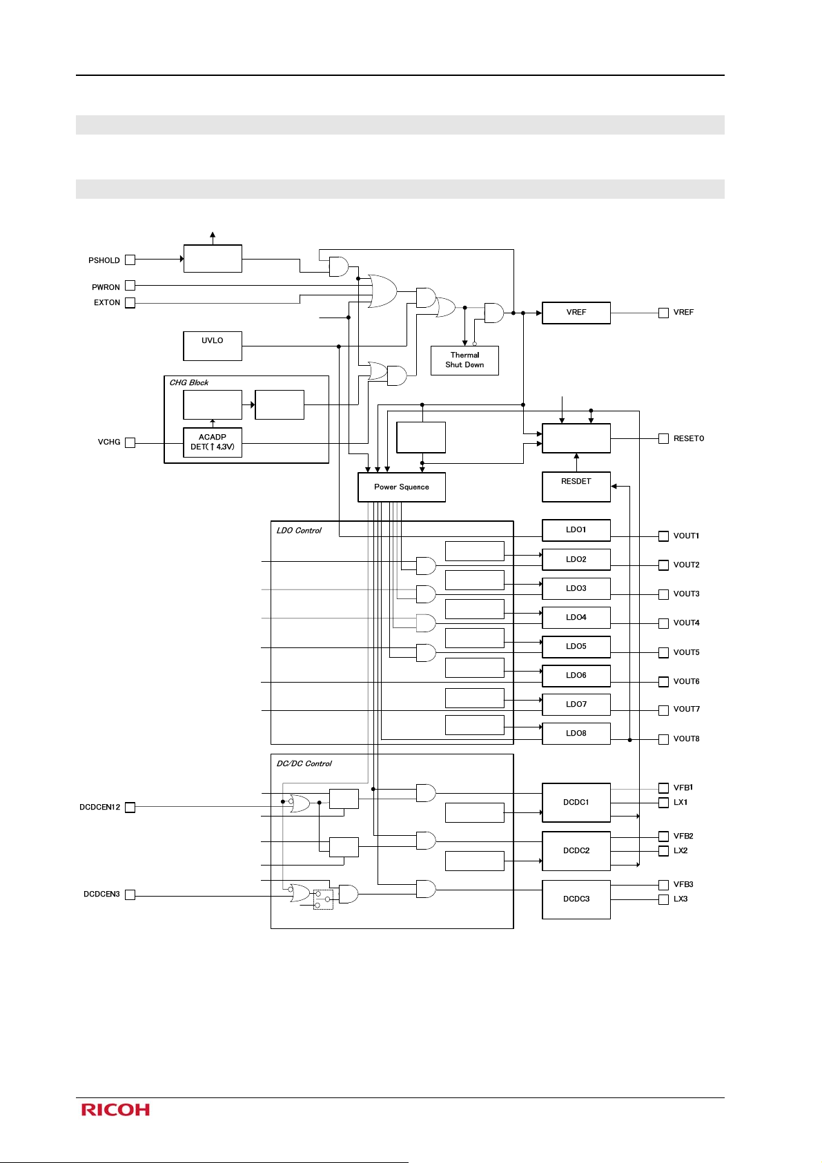
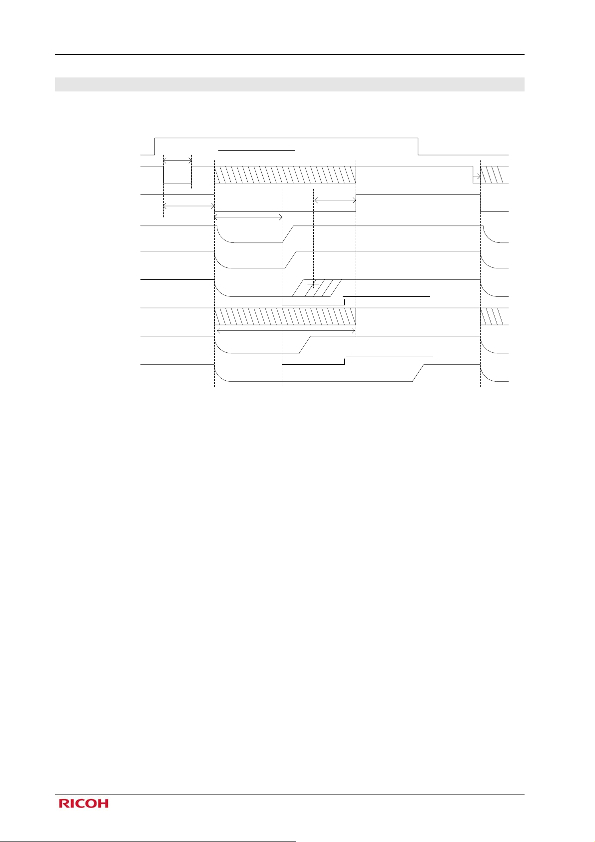
6.2 Power on and off
RN5T614 can be powered on by factors as below.
1. PWRON (external pin)
2. EXTON (external pin)
3. Charging (Shift to Rapid-Charge state)
(a) Power-on by external signal: PWRON (or EXTON) pin
When PWRON pin becomes “H”, the power-on sequence starts synchronizing with the internal clock (32 kHz).
At the same time, ONOB pin becomes “L”.
VREF, DCDC3, LDO2, DCDC1/2, LDO8, LDO5, LDO3, and LDO4 power on following the power-on
sequence in the timing chart below. RESETO released 120ms after LDO8 turns on. After RESETO is released,
PSHOLD is turned to “H” and the power-on state is maintained while PWRON is “H”.
VIN*
VOUT1
PWRON
(or EXTON)
(or Charging)
PSHOLD
VREF
DCDC3(*1)
VOUT8
VOUT5
VOUT3
VOUT4
VOUT2
DCDCEN12
from AP
DCDC1/2
UVLO
Power-on by PWRON(or EXTON or Charging)
0.5ms
12clk
12clk
4clk
4clk
(invalid) (valid)
The power needs to be supplied to VDDIO.
8clk
4clk
0.2ms or more
Holding Power-on
by PSHOLD
Power-on by PWRON
(or EXTON or Charging)
(invalid)
LDO6,7
RESETO
120ms
I2C Enabled
Note*: Internal clk (32kHz±20%)
Note*1: DCDCEN3 pin is invalid by trimming
Fig 6-1 Power-on/off Timing (Sequence2)
©2010-2011 Rev. 1.0 Page 11
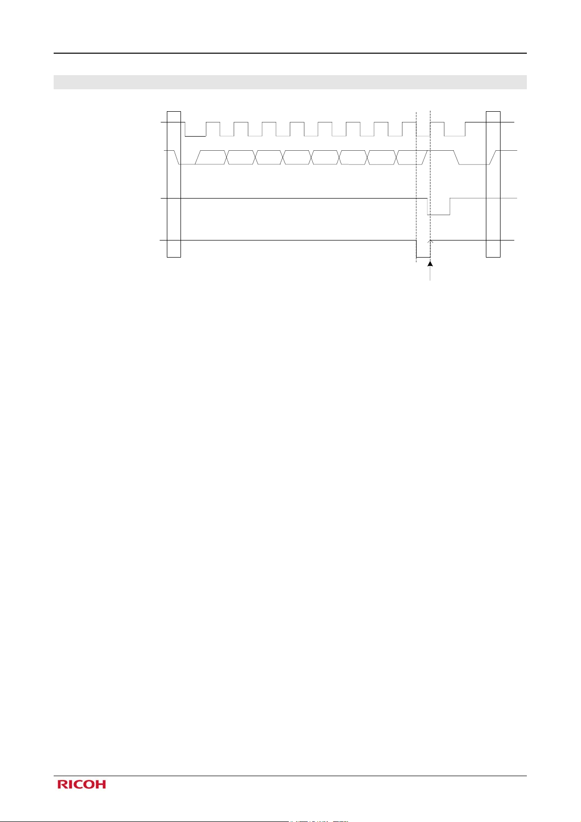
RN5T614 POWER MANAGEMENT SYSTEM DEVICE
PSHOLD can only hold PMIC powered-on but cannot turn on at the timing shown below.
PWRON
Power-on by PWRON(or EXTON or Charging)
(or EXTON)
(or Charging)
PSHOLD
0.5ms
Power-on cannot be carried out
DCDC3
12clk
VOUT8
12clk
VOUT5
4clk
VOUT3
4clk
VOUT4
4clk
VOUT2
8clk
DCDC1,2
by PSHOLD
RESETO
120ms
Note*: Internal clk (32kHz±20%)
(b) Power-off operation
When power-on factor and PSHOLD become "L", all DC/DC and LDO turn off except LDO1 and LDODIG.
©2010-2011 Rev. 1.0 Page 12
RN5T614 POWER MANAGEMENT SYSTEM DEVICE
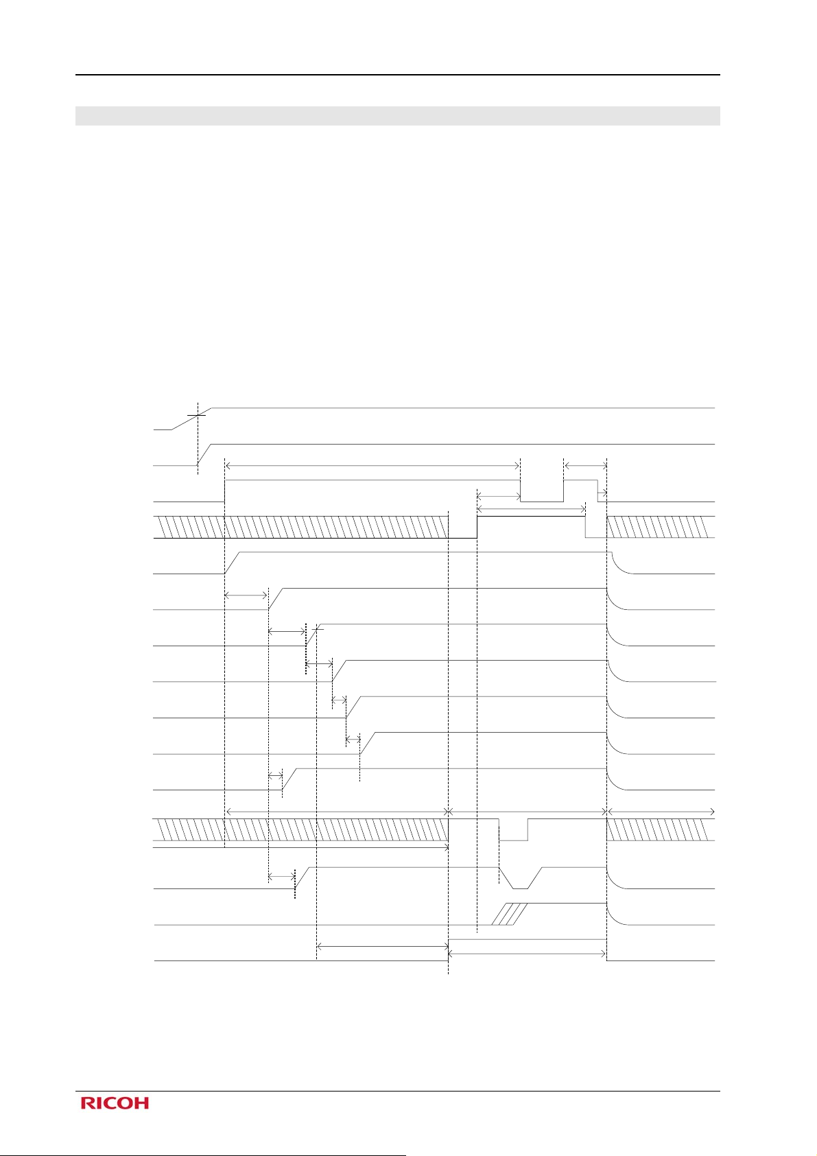
6.3 Soft Reset Operation
PWRON
(or EXTON)
(or Charging)
PSHOLD
0.2ms or more
Soft reset by PSHOLD
RESETO
80ms
320ms
120ms
VREF
DCDC3
8532
4
VOUT8/5/3/4/
2
Power-on Sequence Start
DCDCEN12
DCDC1/2
(invalid)
Power-on Sequence Start
VOUT6/7
Note*: Internal clk (32kHz±20%)
Fig 6-2 Soft Reset Timing
When PWRON becomes “H”, soft reset can be performed by turning PSHOLD to “L”.
When PSHOLD becomes “L”, RESETO outputs “L” after 80ms. And then, all DC/DC and LDO turn off except
LDO1 and LDODIG. DC/DC3 turns on again after 320ms. Then after that, each LDO turns on as the normal
power-on sequence.
©2010-2011 Rev. 1.0 Page 13
RN5T614 POWER MANAGEMENT SYSTEM DEVICE
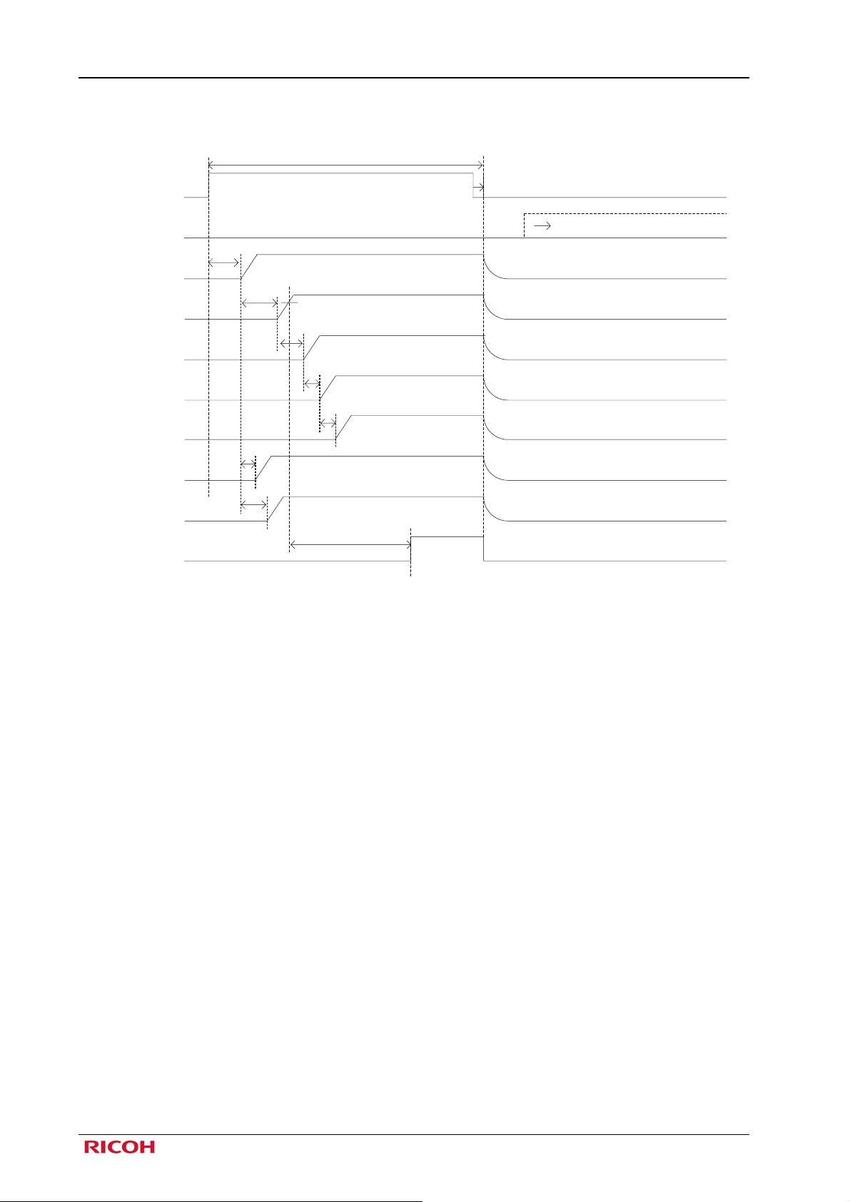
6.4 Stand-by Operation
Fig 6-3 Stand-by Timing
When SLEEP bit is “1”, and power-on factor and PSHOLD become “L”, all DC/DC and LDO turn off (except
LDO1 and LDODIG) with maintaining DC/DC3 turned on. (Note*)
When “H” signal is input to PWRON pin or EXTON pin, the normal power-on sequence starts. SLEEP bit is reset
by UVLO.
Note*: Stand-by operation will not be executed at the following conditions: Soft Reset, RESDET detection, and
latch protection of DC/DC.
©2010-2011 Rev. 1.0 Page 14
RN5T614 POWER MANAGEMENT SYSTEM DEVICE
6.5 UVLO (Under Voltage Lock Out) Electrical Characteristics
When the system cannot operate due to the low battery voltage, UVLO turns off the system (SLEEP bit is reset by
UVLO).
Operating Conditions (unless otherwise specified) T
Symbol Parameter Condition Min Ty p Max Units
V
Under voltage lock out threshold VIN rising 2.8 V
Release
V
Under voltage lock out threshold VIN falling -3% 2.7 +3% V
Detect
V
UVLO Hysteresis - 100 mV
HYS
= 25 degrees C
a
Table 6-1 UVLO Electrical Characteristics
6.6 TSHUT (Thermal Shutdown Circuit) Electrical Characteristics
The thermal shutdown circuit turns off the system and prevents the chip from damaging when overheating is
detected. When the temperature changes back to Return Temperature, the power-on sequence is started again if there
is power-on factor. If there is no power-on factor, the state remains power-off.
Operating Conditions (unless otherwise specified) VIN = 3.6V
Symbol Parameter Condition Min Ty p Max Units
T
DET
T
Return Temperature - 110 degrees C
RET
ISS Supply Current - 7 μA
Detected Temperature - 135 degrees C
Table 6-2 Thermal Shutdown Circuit Electrical Characteristics
©2010-2011 Rev. 1.0 Page 15
RN5T614 POWER MANAGEMENT SYSTEM DEVICE
7. Voltage Detector
7.1 VBAT Detector (VD1) Electrical Characteristics
After VBAT pin rises, BATDET signal turns to “H” after 100ms (Min.) from the VBAT Detector is released.
The default is 3.3V, but it can be changed by the register.
BATDET is Nch-opendrain output pin, and if it is used, pull up the pin with the voltage not exceeding VIN power.
VRelease1
VBAT
VDetect1
BATDET
130ms±30ms
Operating Conditions (unless otherwise specified) T
= 25 degrees C
a
Symbol Parameter Conditions Min. Typ. Max. Units
V
VD1 Threshold Voltage VBAT rising -3% 3.3 (*1) +3% V
Release1
V
VD1 Threshold Voltage VBAT falling 3.1 V
Detect1
V
VD1 Hysteresis - 0.2 V
Hys1
Note*1: The threshold voltage is set by setting the register.
Table 7-1 VD1 Electrical Characteristics
7.2 RESDET Detector (VD2) Electrical Characteristics
The RESDET Detector detects LDO8 voltage.
At the RESDET, “L” is output from RESETO pin. 120ms after RESDET is released, “H” is output.
After RESDET is released, DC/DC and LDO turn off except LDO1 and LDODIG when LDO8 voltage drops lower
than the detection voltage. After DC/DC and LDO are turned off, the power-on sequence is started again if there is
power-on factor. If there is no power-on factor, the state remains power-off.
Operating Conditions (unless otherwise specified) V
= 3.6V, Ta = 25 degrees C
IN
Symbol Parameter Condition Min Typ Max Units
Vout8
V
VD2 Threshold Voltage Vout8 rising
Release2
-3%
×85%
+3% V
(*1)
V
VD2 Hysteresis - 100 mV
Hys2
Note*1: The threshold voltage is set by setting the register.
Table 7-2 RESDET Electrical Characteristics
©2010-2011 Rev. 1.0 Page 16
p
p
(*4)
p
)
p
)
(
)
(
)
(
)
RN5T614 POWER MANAGEMENT SYSTEM DEVICE
8. Regulator
8.1 Regulator Table
DC/DC1 DC/DC2 DC/DC3
Initial Value 1.20V (*1) 1.15V (*2) 1.8V
Output Voltage Range 0.9~1.5V
12.5mVste
Output Current (MAX) 1200mA 1000mA 500mA
External Inductor
2.2μH2.2μH2.2μH
0.9~1.5V,1.8V
12.5mVste
1.8~3.3V
External Capacitor
S
ec-B(*4
Output Control I2C
(with RAMP Control)
ON/OFF Control I2C or DCDCEN12 I2C or DCDCEN12 I2C or DCDCEN3 (*3)
Initial State ON ON ON
For use (Core) (Logic) (Memory)
Note*1: Selected by trimming (Initial Value:1.00/1.10/1.20/1.25/1.30V/1.425V)
Note*2: Selected by trimming (Initial Value:0.95/1.05/1.15/1.20/1.50/1.80V)
Note*3: Selected by trimming (DCDCEN3 pin is valid or invalid)
Note*4: Recommended component
Bypass Capacitors for DC/DC1,2 10uF:C1608JB0J106M(TDK)
Bypass Capacitors for DC/DC3 4.7uF:C1608JB1A475KT(TDK)
Inductor For DCDC1,2 2.2uH:NRH2410T2R2MN(TAIYO-YUDEN)
Inductor For DCDC3 2.2uH:MLP2012S2R2M(TDK)
Input Capacitors for DC/DC 2.2uF:LMK107BJ225KA-T(TAIYO-YUDEN)
10μF10μF4.7μF
I2C
(with RAMP Control)
External R
Table 8-1 Regulator Table (DC/DC)
LDO1 LDO2 LDO3 LDO4 LDO5 LDO6 LDO7 LDO8
Initial Value 3.0V (*1) 1.2V 1.2V 3.3V 1.8V (*1) 2.6V 3.0V 3.3V (*1)
Output Voltage Range - 0.9~1.3V 0.9~1.3V 1.8~3.3V 1.8~3.3V 1.2~3.3V 1.2~3.3V 1.8~3.3V
Output Current (MAX) 10mA 30mA 30mA 300mA 300mA 150mA 150mA 150mA
External Capacitor
S
ec-B(*4
Output Control - I2C I2C I2C I2C I2C I2C I2C
ON/OFF - I2C I2C I2C I2C I2C I2C -
Initial State Keep ON ON (*2) ON (*3) ON (*3) ON (*3) OFF OFF ON
For use (RTC) (Alive)
Note*1: Selected by trimming (LDO1:3.0/1.8V, LDO5:3.0V/1.8V, LDO8:3.0V/3.3V)
Note*2: Selected by trimming (Initial State:Power_on or Keep ON)
Note*3: Selected by trimming (Initial State:Power_on or OFF)
Note*4: Recommended component
Bypass Capacitors for LDO 1uF:GRM155B31A105KE15
1.0μF1.0μF1.0μF1.0μF1.0μF1.0μF1.0μF1.0μF
PLL
(USB OTG) (Memory)
Peripheral
(USB)
MMC
(Host I/F) (LCD) (System)
Table 8-2 Regulator Table (LDO)
©2010-2011 Rev. 1.0 Page 17
RN5T614 POWER MANAGEMENT SYSTEM DEVICE
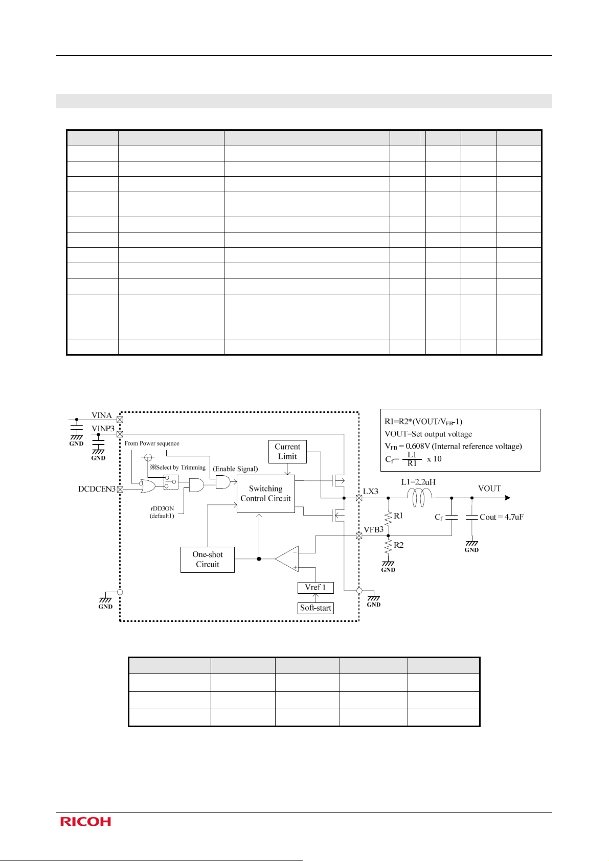
8.2 Step-down DC/DC Converter
RN5T614 has two PWM/PFM/PSM step-down DC/DC converters and one One-shot PWM DC/DC converter. They
employ external inductor and capacitor for smoothing output voltage. DC/DC3 sets output voltage by the external
resistance.
8.2.1 Step-down DC/DC1 and DC/DC2 Converte r
RN5T614 has CMOS-based PWM/PFM/PSM step-down DC/DC1 (DC/DC2) converter with a low supply current.
PWM/PFM/PSM mode is controlled in two methods. One is AUTO mode that automatically switches PWM/PFM, and
the other is the register setting that sets AUTO/PWM/PSM through I2C. The output voltage is also programmable by
DD1DAC (DD2DAC) register.
Since DD1MODE (DD2MODE) bit and DD1DAC (DD2DAC) are reset when DC/DC1 (DC/DC2) turns off, the next
activation starts at 1.20V that is the default of DD1DAC (1.15V that is the default of DD2DAC).
DC/DC1 and DC/DC2 converters have RAMP control function.
RN5T614 integrates the latch protection function to avoid any malfunctions by over current. The current limit circuit
monitors over current with LX1 (LX2) clock cycle.
When over current is detected and continues for a certain time (10ms), RESETO outputs “L”. And then, all DC/DC and
LDO turn off except LDO1 and LDODIG.
After DC/DC and LDO are turned off, the power-on sequence is started again if there is power-on factor. If there is no
power-on factor, the state remains power-off.
DC/DC1 and DC/DC2 converters can be easily composed with only few external components such as inductor,
capacitor and etc. For the output capacitor, the ceramic type should be used for reducing the ripple voltage.
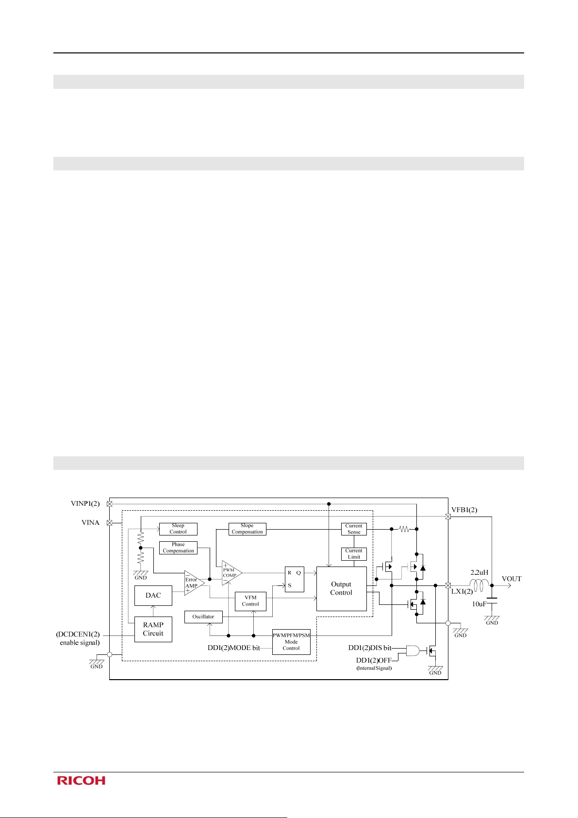
8.2.1.1 Step-down DC/DC1 and DC/DC2 Conve r te rs Bl ock Diagram
Fig 8-1 Step-down DC/DC1 and DC/DC2 Converter Block Diagram
©2010-2011 Rev. 1.0 Page 18
RN5T614 POWER MANAGEMENT SYSTEM DEVICE
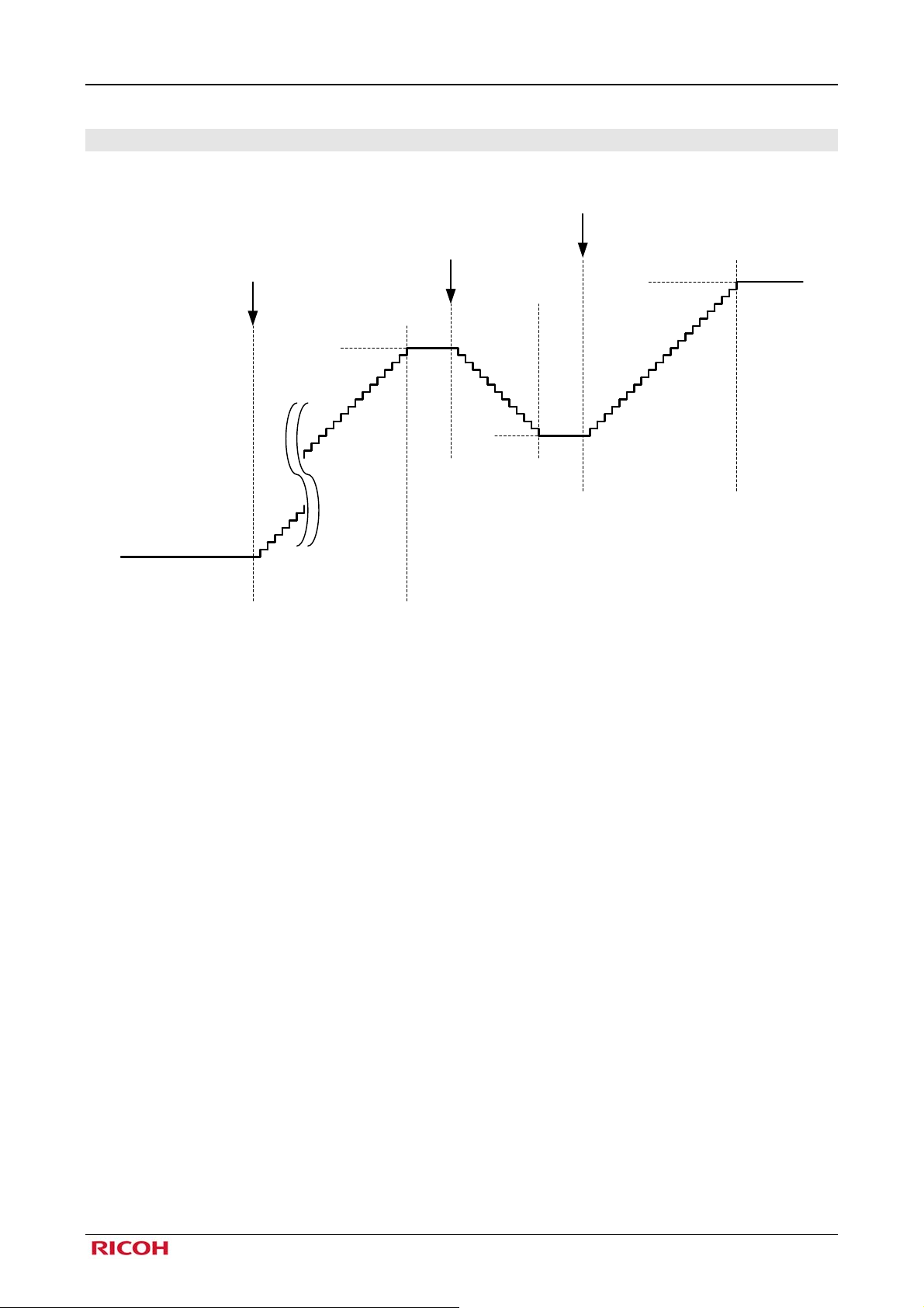
8.2.1.2 RAMP Control Operation
This function starts by setting DD1(2)DAC register. The ramp rate is controllable by RAMP1(2)SLOP bit.
Set DD1(2)DAC register
Set DD1(2)DAC register
Enable
DC/DC1(2)
Output Voltage
Output Ramp Rate
Output Ramp Rate
Soft Start Slew Rate
Fig 8-2 Ramp up/down Control Timing Chart
©2010-2011 Rev. 1.0 Page 19
RN5T614 POWER MANAGEMENT SYSTEM DEVICE
8.2.1.3 Step-down DC/DC1 and DC/DC2 Converter Electrical Characteristics
Operating Conditions (unless otherwise specified) V
= 3.6V, L=2.2μH, C
IN
= 10μF, Ta = 25 degrees C
OUT
Symbol Parameter Condition Min Typ Max Units
VIN Input voltage range - 3.1 3.6 5.5 V
V
OUT
Vaccu
-40 degrees C < T
Range of output voltage
Voltage setting step width
Output voltage accuracy
1mA < I
3.1V < V
< Ilx,
OUT
< 5.5V
IN
< 85 degrees
a
DC/DC1
DC/DC2
PFM/PSM
Mode
PWM
Mode
1mA < I
OUT
1mA < I
OUT
-
V
=0.9V~1.0V
OUT
V
=1.0V~1,5V,1.8V
OUT
V
=0.9V~1.0V
OUT
V
=1.0V~1.5V,1.8V
OUT
< 1200mA
< 1000mA
0.9 1.20 1.5
V
0.9
1.15
1.8
12.5 mV
-27 8.5 44 mV
-2.5 1 4.5 %
-35 35 mV
-3.5 3.5 %
Vrip Output ripple voltage PFM/PSM Mode Iout=1mA 25 mV
ΔV
OUT
/ΔTa
Output voltage temperature
coefficient
-40 degrees C < Ta < 85 degrees C ±100
ppm/
degreesC
Fosc Switching frequency - 2.2 MHz
Ilx Maximum output current
Ilim Limit current
Vpeak Output transition response
Tprot Protection delay time
Iss Consumption current
DC/DC1(AUTO/PWM Mode)
DC/DC2(AUTO/PWM Mode)
DC/DC1,2(PSM Mode)
DC/DC1
DC/DC2
10→500mA@ΔT=1μs, V
OUT
-
AUTO Mode I
PSM Mode I
V
= 1.20V, I
OUT
OUT
OUT
OUT
=0mA
=0mA
=1mA
=1.2V
1200 mA
1000 mA
10 mA
1800 mA
1500 mA
50 mV
10 ms
50 μA
25 μA
75 %
Η1 Efficiency peak
V
= 1.20V, Iout =η_peak
OUT
85 %
Table 8-3 DC/DC1 and DC/DC2 Electrical Characteristics
©2010-2011 Rev. 1.0 Page 20
RN5T614 POWER MANAGEMENT SYSTEM DEVICE
8.2.2 Step-down DC/DC3 Converter Electrical Characteristics
Operating Conditions (unless otherwise specified)
Symbol Parameter Condition Min Typ Max Units
VIN
V
OUT
Ilx Maximum output current
Iss
I
OFF
Ilim
VFB
ΔVFB/ΔVIN
ΔVFB/ΔIlx
ΔVFB/ΔTa
tr Soft-start Time - 120 μs
Input Voltage Range
Output Voltage Range
Consumption Current
Standby Current
Limit detection Current
FB Voltage
FB Line Regulation
FB Load Regulation
FB Voltage
Temperature Coefficient
V
OUT
-40 degrees C≦Ta≦+85 degrees C
VIN = 3.6V, L=2.2μH, C
3.1V≦VIN≦5.5V
= VFB =3.6V
V
IN
Ilx =0mA, no switching
OFF state
-
VIN = VFB =3.6V, Ilx =1mA
+0.5≦VIN≦5.5V, Ilx = Ilxmax / 2
1mA≦Ilx≦500mA
OUT
= 4.7μF, Ta = 25 degrees C
3.1 5.5 V
1.8 3.3 V
500 mA
70 μA
1 μA
800 mA
-1.5% 0.608 +1.5% V
10 mV
2 mV
±100
Table 8-4 DC/DC3 Electrical Characteristics
ppm/
degrees
C
Fig 8-3 DC/DC3 Block Diagram
Output Voltage R1 R2 Cf Notes
3.3V 120kΩ 27kΩ 180pF
2.5V 150kΩ 47kΩ 150pF
1.8V 220kΩ 110kΩ 100pF
Table 8-5 DC/DC3 External Components Example
©2010-2011 Rev. 1.0 Page 21
RN5T614 POWER MANAGEMENT SYSTEM DEVICE
8.3 LDO
RN5T614 has eight LDOs. LDO1 for RTC is always on, and it has the reverse-current prevention circuit.
VREF circuit is only for the internal reference voltage, so it cannot be used as the external reference voltage.
For optimized phase compensation, the bypass capacitor must be the ceramic type.
8.3.1 LDO Electrical Characteristics
8.3.1.1 LDO1 Electrical Characteristics
Operating Conditions (unless otherwise specified) V
Symbol Parameter Condition Min Typ Max Units
VIN Input Voltage Range - 3.1 3.6 5.5 V
V
Output Voltage (*2)
OUT
I
Output Current - 10 mA
OUT
I
SHT
ΔV
/ΔVIN Line Regulation
OUT
ΔV
/ΔI
OUT
OUT
Short Current
Load Regulation
Output Voltage
ΔV
OUT
/ΔTa
Temperature
Coefficient
ISS Supply Current (*1) ON 1 3 μA
IRR Reverse Current V
3.1V≦V
50μA≦I
+0.2V≦VIN≦5.5V
V
OUT
I
OUT=IOUTMAX
50μA≦I
-40 degrees C≦T
=3.0V & VIN =0V 0.15 μA
OUT
= 3.6V, C
IN
≦5.5V
IN
≦10mA
OUT
V
=0V 30 mA
OUT
/2
≦10mA
OUT
≦85 degrees C
a
= 1.0μF, Ta = 25 degrees C
OUT
-3%
3.0 /
1.8
3
30 mV
±100
+3% V
mV
degrees C
ppm/
Table 8-6 LDO1 Electrical Characteristics
Note*: Bypass capacitor: 1.0μF, in mounted state.
For optimized phase compensation, the bypass capacitor must be the ceramic type.
Note*1: The consumption current of the reverse protection is not included.
Note*2: Initial value selected by trimming (3.0V or 1.8V)
©2010-2011 Rev. 1.0 Page 22

RN5T614 POWER MANAGEMENT SYSTEM DEVICE
8.3.1.2 LDO2 and LDO3 Electrical Characteristics
Operating Conditions (unless otherwise specified) VIN = 3.6V, C
Symbol Parameter Condition Min Ty p Max Units
VIN Input Voltage Range - 3.1 3.6 5.5 V
V
OUT
I
OUT
I
Short Current
SHT
ΔV
/ΔVIN Line Regulation
OUT
ΔV
/ΔI
OUT
ΔV
OUT
Output Voltage Range
Output Current - 30 mA
OUT
Load Regulation 50μA≦I
Transient Response 50μA⇔I
3.1V≦V
50μA≦I
3.1V≦V
I
OUT
OUTMAX
V
= I
Output Voltage
ΔV
OUT
/ΔTa
Temperature
-40 degrees C≦Ta≦85 degrees C ±100
Coefficient
RR Ripple Rejection
EN Output Noise (RMS)
ISS Supply Current
I
Standby Current
OFF
Tr
Tf
V
SET
Rising Time
Falling Time
Programmable
Output Voltage
f=10kHz, I
BW=100Hz-100kHz, I
I
OUT
I
OUT
V
≧0.7×V
OUT
V
≦0.3×V
OUT
I
= I
OUT
= 1.0μF, Ta = 25 degrees C
OUT
≦5.5V,
IN
OUT≦IOUTMAX
=0V
OUT
≦5.5V,
IN
/2
OUTMAX
OUT≦IOUTMAX
-3%
65 mA
30 mV
0.9
~1.3
+3% V
/2 (⊿t=1us) 50 mV
OUT
= I
/ 2 60 dB
OUTMAX
OUT
= I
/ 2 50 μVr ms
OUTMAX
=0mA 20 μA
=0mA 1 μA
, I
OUT
OUT
=0mA 200 μs
OUT
, I
=0mA 500 μs
OUT
0.9
1.0
OUTMAX
/2
-3%
1.1
+3% V
1.2
1.3
10 mV
ppm/
degrees C
Table 8-7 LDO2 and LDO3 Electrical Characteristics
Note*: Bypass capacitor: 1.0μF, in mounted state.
For optimized phase compensation, the bypass capacitor must be the ceramic type.
©2010-2011 Rev. 1.0 Page 23

RN5T614 POWER MANAGEMENT SYSTEM DEVICE
8.3.1.3 LDO4 and LDO5 Electrical Characteristics
Operating Conditions (unless otherwise specified) VIN = 3.6V, C
Symbol Parameter Condition Min Typ Max Units
Input Voltage Range
Output Voltage Range
Output Current
Short Current V
Line Regulation
Load Regulation
OUT
Transient Response
Voltage difference
+0.3V≦VIN≦5.5V &
V
OUT
3.1V≦V
50μA≦I
+0.3V≦VIN≦5.5V &
V
OUT
3.1V≦V
50μA≦I
50μA⇔I
V
>3.1V, VIN = V
IN
OUT≦IOUTMAX
OUT
I
= I
OUT
OUT≦IOUTMAX
OUTMAX
ΔV
ΔV
VIN -V
V
I
OUT
OUT
ΔV
VIN
OUT
I
OUT
SHT
/ΔVIN
/ΔI
OUT
OUT
Output Voltage
ΔV
OUT
/ΔTa
Temperature
-40 degrees C≦Ta≦85 degrees C
Coefficient
≦3.0V, f=10kHz,
V
V
OUT
V
OUT
OUT
I
= I
OUT
I
OUT
I
OUT
≧0.7×V
≦0.3×V
= I
I
OUT
RR Ripple Rejection
EN Output Noise (RMS)
BW=100Hz-100kHz, I
ISS Supply Current
I
Standby Current
OFF
Tr
Tf
V
SET
Rising Time
Falling Time
Programmable
Output Voltage
= 1.0μF, Ta = 25 degrees C
OUT
-
≦5.5V,
IN
-
3.1 3.6 5.5 V
-3%
1.8
~3.3
+3% V
300 mA
= 0V 75 mA
≦5.5V,
IN
/2
OUTMAX
/2(⊿t=1us)
, I
SET
OUT
= I
OUTMAX
10 mV
60 mV
100 mV
0.3 V
±100
OUTMAX
OUT
=0mA
=0mA
, I
OUT
, I
OUT
/ 2
= I
OUT
OUT
OUTMAX
=0mA
=0mA
/ 2
60 dB
75 μVrms
20 μA
1 μA
200 μs
500 μs
1.80
2.50
2.60
OUTMAX
/2
-3%
2.80
+3% V
2.85
3.00
3.30
ppm/
degrees C
Table 8-8 LDO4 and LDO5 Electrical Characteristics
Note*: Bypass capacitor: 1.0μF, in mounted state.
For optimized phase compensation, the bypass capacitor must be the ceramic type.
©2010-2011 Rev. 1.0 Page 24

RN5T614 POWER MANAGEMENT SYSTEM DEVICE
8.3.1.4 LDO6, LDO7 and LDO8 Electrical Characteristics
Operating Conditions (unless otherwise specified) V
Symbol Parameter Condition Min Ty p Max Units
VIN Input Voltage Range -
V
Output Voltage Range
(*1)
Output Current -
Line Regulation
Load Regulation 50μA≦I
OUT
Transient Response 50μA⇔I
Voltage difference V
ΔV
ΔV
VIN -V
V
OUT
I
OUT
I
Short Current
SHT
/ΔVIN
OUT
/ΔI
OUT
ΔV
OUT
OUT
Output Voltage
ΔV
OUT
/ΔTa
Temperature
Coefficient
RR Ripple Rejection
EN Output Noise (RMS)
ISS Supply Current
I
Standby Current
OFF
Tr
Tf
Rising Time
Falling Time
Programmable
V
SET
Output Voltage
(*1)
OUT
50μA≦I
V
OUT
>3.1V, VIN = V
IN
-40 degrees C≦Ta≦85 degrees C
BW=100Hz-100kHz, I
V
OUT
V
OUT
= 3.6V, C
IN
OUT
+0.3V≦VIN≦5.5V &
3.1V≦V
≦5.5V,
IN
OUT≦IOUTMAX
= 0V 75
V
OUT
+0.3V≦VIN≦5.5V &
3.1V≦V
I
OUT
V
OUT
I
OUT
≧0.7×V
≦0.3×V
I
OUT
≦5.5V,
IN
= I
OUT≦IOUTMAX
OUTMAX
/2
OUTMAX
/2(⊿t=1us)
, I
SET
OUT
= I
≦3.0V, f=1kHz,
I
I
= I
OUT
OUT
= I
OUTMAX
OUT
=0mA
=0mA
, I
OUT
, I
OUT
OUTMAX
/ 2
= I
OUT
OUT
/2
=0mA
=0mA
OUTMAX
= 1.0μF, Ta = 25 degrees C
3.1 3.6 5.5
1.2
~3.3
150
10
40
50
0.3
±100
60
85
20
1
200
500
1.20
1.80
2.50
2.60
2.80
2.85
3.00
3.30
OUTMAX
-3%
/ 2
-3%
+3%
+3%
V
V
mA
mA
mV
mV
mV
V
ppm/
degrees C
dB
μVrm s
μA
μA
μs
μs
V
Table 8-9 LDO6, LDO7 and LDO8 Electrical Characteristics
Note*: Bypass capacitor: 1.0μF, in mounted state.
For optimized phase compensation, the bypass capacitor must be the ceramic type.
Note*1: 1.2V setteing except LDO8
©2010-2011 Rev. 1.0 Page 25
RN5T614 POWER MANAGEMENT SYSTEM DEVICE
9. Li-ion Battery Charger
RN5T614 integrates a Li-ion Battery charger.
---It supports AC adapter charging.
---With the current limit protection and charge current control, the limited power can be efficiently supplied to the
system and the battery.
---The system can power on even when Li-ion Battery is low voltage or open.
---The device can withstand up to 6.5V on VCHG pin. However, it can withstand high voltage by combining a high
voltage protection IC (up to 28V by using BD6040 of ROHM).
---Rapid timer and Trickle timer integrated.
---Monitor for the battery thermistor built in.
---No external MOSFET required.
---If the system loads over AC adapter current rating, the battery will supply the current to the system.
---Chip temperature detection circuit for over temperature protection integrated.
---Ibat maximum tolerant current: 1.2A
9.1 Li-ion Battery Charger Block Diagram
AC Adapter
OVP
(BD6040)
VCHG
VSYS
CHGLED
VCHGREG
GND
VCHGDET
REG
Fig 9-1 Li-ion Battery Charger Block Diagram
Itotal Isys
SW1
CURRENT
LIMIT
control
Charger SW
control
Charge
Control
Logic
Thermistor
Monitor
REG
SW2
VSYS
IbatIchg
VBAT
THERMBAT
VTHM
IMONI
To system load
(VINxx)
Li-ion Battery
T
©2010-2011 Rev. 1.0 Page 26

RN5T614 POWER MANAGEMENT SYSTEM DEVICE
9.2 Explanation of Charge Block Operating
If AC adapter is connected to VCHG pin, the charger detects the voltage on VCHG pin.
4.3V < V
If the voltage is as above, the charger will operate.
If the voltage is other than the above, the charger will not operate.
When (1), the charger switches the power source between VCHG and VBAT when it is in the state of Charge-Ready or
Trickle Charge or Rapid-Charge and also it satisfies the following conditions.
Temperature < 125 degrees C (Programmable)
The charger implements the means of checking the presence of the battery. If it detects no battery, the power of VSYS is
supplied by VCHG until the battery is detected.
It is assumed that AC adapter voltage is 5V within 10%. Other values of voltage are not recommended because the die
temperature rises due to the generated heat by increasing the voltage of AC adapter.
The current limit of SW1 is set by the register as below.
Ilim > Ichg
The value of the register set for the current limit of SW1 is set lower than the current capacity of AC Adapter.
Note*: Initial value of current limit of SW1 is 720mA.
CHGLED pin is the Nch-open-drain output.
It turns on at the Rapid-Charge state and turns off at the Charge Complete.
At the Trickle-Charge or Abnormal state, it flashes on and off at 1-2Hz.
< 6.2V (1)
VCHG
©2010-2011 Rev. 1.0 Page 27

RN5T614 POWER MANAGEMENT SYSTEM DEVICE
Li-ion Battery Charger state Diagram
Charge Off
Adapter Connection
(4.3V < VCHG < 6.2V)
Charge Ready
<CHGSTART>=”1”
No Adapter
(VCHG<4.0V)
<SUSPENDB>=”1”
<SUSPENDB>=”0”
SUSPEND
<CHGSTART>=”0”
VBAT>3.0V VBAT<2.9V
<CHGSTART>=”0”
Rapid Timer Time-up
or
Charge Complete
( VBAT>4.1V & Ichg<Icomp
& Die temperature not detected )
<CHGSTART>=”0”
Fig 9-2 Li-ion Battery Charger State Flow (Normal State)
Trickle Charge
Rapid Charge
Charge Complete
Charging Normal State
<SUSPENDB>=”0”
<SUSPENDB>=”0”
Not Full Battery
(VBAT<4.0V)
<SUSPENDB>=”0”
©2010-2011 Rev. 1.0 Page 28

RN5T614 POWER MANAGEMENT SYSTEM DEVICE
Li-ion Battery Charger state Diagram (Abnormal)
Adapter Over Voltage
Normal State
SUSPEND
Normal State
(VCHG > 6.2V)
<SUSPENDB>=”0”
Battery Over Voltage
(VBAT>4.6V)
Adapter Over
Voltage
Battery Over
Voltage
Adapter Over Voltage
(VCHG > 6.2V)
No Battery
Trickle Charge
Charge Ready
Normal State
Charging State
Previous Charging State
(SUSPEND state
changes back to
Charge Ready state)
Trickle Timer Time-up
Battery Connection
No Battery
Battery Temperature NG
Battery Temperature OK
Battery Error
No Battery
No Battery
No Battery
Battery Temperature
Error
Adapter Over Voltage
(VCHG > 6.2V)
Adapter Over Voltage
(VCHG > 6.2V)
Adapter Over Voltage
(VCHG > 6.2V)
Fig 9-3 Li-ion Battery Charger State Flow (Abnormal State)
©2010-2011 Rev. 1.0 Page 29

RN5T614 POWER MANAGEMENT SYSTEM DEVICE
[Charge-Off]
The power is supplied by battery through VSYS pin:
・When a power supply device is not connected to VCHG pin.
・When V
is lower than 4.3V.
VCHG
[SUSPEND]
The state changes to SUSPEND by writing "0" into SUSPENDB bit when the state is Charge Ready, Trickle charge,
Rapid Charge, or Charge Complete. When the state is SUSPEND, the battery is not charged and VSYS is supplied by
the current from the battery.
The state changes to Charge Ready by writing "1" into SUSPENDB bit.
SUSPENDB bit is set to "1" automatically and unable to set to "0" except when the state is Charge-Off,
Adapter-Over-Voltage, SUSPEND, Charge-Ready, Trickle-Charge, Rapid-Charge and Charge-Complete.
[Charge-Ready]
When VCHG pin voltage exceeds 4.3V, the state shifts from Charge-Off to Charge-Ready.
When "0" is set to CHGSTART bit at Trickle-Charge, Rapid-Charge, or Charge-Complete state, it returns to
Charge-Ready state, and the charging stops.
[Trickle-Charge]
When CHGSTART bit is “1”, the state shifts form Charge-Ready to Trickle-Charge.
If the battery voltage is less than 3.0V in Rapid-Charge, the state shifts to Trickle-Charge.
In Trickle-Charge state, Ichg is limited to 100mA.
The battery charging continues until V
becomes over 3.0V or Trickle-Timer is up. If the battery voltage becomes
VBAT
over 3.0V, the state shifts to Rapid-Charge. If Trickle-Timer is up before completing the trickle charge, the state shifts to
Battery-Error, and the charger outputs the interrupt signal.
[Rapid-Charge]
Even when the power is supplied to the system through VCHG pin, the battery charging is still performed. The battery
charge current is adjusted depending on the system load. If Itotal is lower than Ilim, the charger automatically increases
Ichg gradually to the value set by register. On the other hand, if Itotal is higher than Ilim, the charger decreases Ichg
immediately. The battery charging continues until three conditions as below are all met or Rapid-Timer is up.
1. Ichg < Icomp
2. V
VBAT
> 4.1V
3. Die temperature not detected
In Rapid-Charge state, the battery charging is automatically performed.
When the charger detects the die temperature higher than the setting value during charging, Ichg is decreased to the
lowest current.
[Charge-Complete]
When the charging is completed, the state shifts to Charge-Complete.
When V
becomes under 4.0V, the state shifts to Rapid-Charge.
VBAT
In the state of Charge-Complete, the power is supplied to VSYS pin only by VCHG pin.
©2010-2011 Rev. 1.0 Page 30

RN5T614 POWER MANAGEMENT SYSTEM DEVICE
[Battery-Error]
User must confirm whether the connection situation of battery is right or not.
[No-Battery]
In any states except Adapter-Over-Voltage and Charge-Off state, when the thermistor monitoring circuit detects no
battery, the state shifts to No-Battery, and the power is supplied only through VCHG pin until the battery is detected.
[Adapter-Over-Voltage]
The charger integrates a detector for the power supply device voltage. If the charger detects that V
6.2V at any states, it supplies the power only from the battery to VSYS pin until V
becomes lower than 4.0V.
VCHG
is higher than
VCHG
However, if the conditions for the transition to Battery-Over-Voltage, Battery-Error, No-Battery, and
Battery-Temperature-Error state are satisfied at the same time, the power is supplied only through VCHG pin. And
SUSPENDB bit is set to “1” automatically and unable to set to “0”.
[Battery-Over-Voltage]
The charger integrates a detector for the battery voltage. If the charger detects that V
is higher than 4.6V at any
VBAT
states except Charge-Off, it supplies the power only through VCHG pin until the battery is disconnected.
[Battery-Temperature-Error]
The voltage of THERMBAT pin is always monitored. If the voltage becomes over 73% or under 23% of VTHM voltage
set by VBTEMP, the battery temperature is determined as abnormal, and the state shifts to Battery-Temperature-Error.
In Battery-Temperature-Error state, except Charge-Off and Adapter-Over-Voltage, both charging for the battery and
power supply from the battery to VSYS stop and the current supply for VSYS is only from the adapter.
If the voltage of THERMBAT pin recovers to the normal range, the state shifts to the one before the transition to
Battery-Temperature-Error state.
©2010-2011 Rev. 1.0 Page 31

RN5T614 POWER MANAGEMENT SYSTEM DEVICE
9.3 Charge Interrupt Request
The charger outputs INTB pin. All interrupt requests can be masked/unmasked by setting the register.
Interrupt request list and details
・ADPDET Adapter insert & remove
・DIEOT Die abnormal temperature by SW1 or SW2 in charger
・VBTERR Battery abnormal temperature
・NOBATT No Battery detect
・VCOV Adapter over voltage (V
・VBOV Battery over voltage (V
・STCR Shift to Charge-Ready state
・STRC Shift to Rapid-Charge state
・CHGCMP Charge complete
・TIMEOUT Time out of Trickle Time or Rapid Timer
Note*: DIEOT, VBTERR and NOBATT are Level interrupt requests.
On the other hand, the other interrupts are generated only when the interrupts appear.
For the details of interrupt, refer to Chapter 10 Interrupt Controller (INTC).
VCHG
VBAT
>6.2V)
> 4.6V)
©2010-2011 Rev. 1.0 Page 32

RN5T614 POWER MANAGEMENT SYSTEM DEVICE
9.4 Li-ion Battery Charger Electrical Characteristics
Operating Conditions (unless otherwise specified) V
VCHG
= 5.0V, V
= 4.8V, V
VSYS
= 3.6V, Ta = -40~85 degrees C
VBAT
Symbol Parameter Setting Condition Min Typ Max Unit
POWER INPUT
V
AC Adapter Input Voltage
VCHG
V
VSYS Regulation Voltage
VSYS
Operating voltage 4.3 6.2 V
Recommended voltage 4.5 5 5.5 V
V
=5.5V,
VCHG
Itotal=500mA,
4.65 4.8 4.95 V
Ta=-10~60 degrees C
Ilim Current Limit
V
V
ADET
R
AOV
SW1
AC Adapter Detection
AC Adapter Over Voltage
Voltage
detection
Hysteresis
Dropout Resistance
120mA
240mA
360mA
480mA
V
=5V,
600mA
720mA *
VCHG
V
=4V,
VSYS
Ta=-10~60 degrees C
840mA
960mA
1080mA
1200mA
Rising 4.15 4.3 4.45
-
- 5.8 6.2 6.5 V
V
=4.7V,
VCHG
Itotal=500mA,
84 102 120
192 216 240
288 324 360
384 432 480
480 540 600
576 648 720
672 756 840
768 864 960
864 972 1080
960 1080 1200
0.3
200 500 mohm
Ta=-10~60 degrees C
VOL
“L” Output Voltage
IOZ Off Leakage Current
CHGLED
I
= 10mA
SINK
VIN=0~V
VSYS
,
Pin= CHGLED
0.4 V
-3 3 μA
mA
V
Table 9-1 Battery Charger Electrical Characteristics (POWER INPUT)
Note*: “*” is the initial value. The set value is changed by setting the register.
©2010-2011 Rev. 1.0 Page 33

RN5T614 POWER MANAGEMENT SYSTEM DEVICE
Operating Conditions (unless otherwise specified) V
VCHG
= 5.0V, V
= 4.8V, V
VSYS
= 3.6V, Ta = -40~85 degrees C
VBAT
Symbol Parameter Setting Condition Min Typ Max Unit
BATTERY CHARGER
V
Battery Charge Voltage
BCHG
Ichg Rapid Charge Current
Itri Trickle Charge Current
Icomp Charging Completion Current
V
V
V
V
RCHG
CCMP
BOV
BTEMP
Rapid Charging Threshold
Charging Completion Voltage
Voltage
(Re-Charging Voltage)
Battery Over Voltage detection
THERMBAT Threshold
4.2V *
4.12V
4.07V
100mA
200mA
300mA
400mA
500mA *
600mA
700mA
800mA
900mA
100mA
25mA *
50mA
75mA
100mA
125mA
150mA
175mA
200mA
Rising
Hysteresis
Rising
Hysteresis
Low Temperature
High Temperature
Ta=-10~60 degrees C,
Ichg=25mA
Ta=-10~60 degrees C
Ta=-10~60 degrees C
Ta=-10~60 degrees C
Ta=-10~60 degrees C
Ta=-10~60 degrees C
- 4.5 4.6 4.7 V
Ratio of VTHM Voltage
4.17 4.2 4.23 V
4.085 4.12 4.155 V
4.035 4.07 4.105 V
70 85 100 mA
100 150 200 mA
200 250 300 mA
300 350 400 mA
400 450 500 mA
400 500 600 mA
500 600 700 mA
600 700 800 mA
700 800 900 mA
70 85 100 mA
25 mA
50 mA
75 mA
100 mA
125 mA
150 mA
175 mA
200 mA
2.9 3 3.1
0.1
4.05 4.1 4.15
0.1
73 %
23 %
105
115
125
degrees C
135
T
DTEMP
Die Temperature Control
Threshold
Detection Temperature
(Programmable)
V
V
R
On Resistance
SW2
Ttri
Timer
Trap
Ibatmax Ibat maximum tolerant current
Trickle Timer
Rapid Timer
Power supply
current from Li-ion
battery
Hysteresis 20
V
=4.2V, Ibat=1A 60 120 mohm
VBAT
Ta=-10~60 degrees C
3.4V < V
VBAT
Table 9-2 Battery Charger Electrical Characteristics (BATTERY CHARGE)
Note*: “*” is the initial value. The set value is changed by setting the register.
©2010-2011 Rev. 1.0 Page 34
40 min
120 * min
< 4.2V 1.2 A

RN5T614 POWER MANAGEMENT SYSTEM DEVICE
10. Interrupt Controller (INTC)
RN5T614 has an interrupt controller (INTC).
CPU can read all the permitted interrupt request flags coming from different functional blocks. When an interrupt
occurs, CPU is informed by asserting INTB pin and reading Monitor register (MON_***) to identify which block is
producing the interrupt. Monitor register is read-only. OR gate signal of each permitted interrupt request flag (IR_***)
will be output from INTB pin.
CPU can figure out the current state of RN5T614 by reading Monitor register at power-on. To enable interrupt output
through INTB pin, it is necessary to write “1” in Enable register (EN_***).
10.1 Interrupt Controller Block Diagram
Local Block
10
Both Edge Type
Interrupt Request
Clear Pulse
Rising Edge Type
Interrupt Request
Clear Pulse
ADPDET,DIEOT,VBTERR,NOBATT,
VCOV,VBOV,STCR,STRC,CHGCMP,
TIMEOUT
Monitor
(MON_***)
Both Edge
Detector
Monitor
(MON_***)
Rising Edge
Detector
INTC
Both Edge Type
Rising Edge Type
Level Type
Request Flag
(IR_***)
Enable
(EN_***)
Request Flag
(IR_***)
INTBCharger
Enable
Level Type
Monitor
(MON_***)
(EN_***)
Interrupt Request
Request Flag
Clear Pulse
Fig 10-1 INTC Block Diagram
©2010-2011 Rev. 1.0 Page 35
(IR_***)
Enable
(EN_***)

RN5T614 POWER MANAGEMENT SYSTEM DEVICE
10.2 Interrupt Timing Chart
Both Edge Type
Interrupt Request
MON_***
IR_***
EN_***
INTB pin
Rising Edge Type
Interrupt Request
MON_***
IR_***
EN_***
INTB pin
clear the flag
by writing register
clear clear
set set
clear the flag
by writing register
clear clear
set set
clear the flag
by writing register
set
clear the flag
by writing register
Level Type
Interrupt Request
MON_***
IR_***
EN_***
INTB pin
not accept
clear command
by register access
set set
clear the flag
by writing register
clear clear
clear the flag
by writing register
Fig 10-2 Interrupt Timing Chart
©2010-2011 Rev. 1.0 Page 36

RN5T614 POWER MANAGEMENT SYSTEM DEVICE
10.3 Interrupt Request List
CHARGER
Block Interrupt Request
ADPDET Both Edge EN_ADPDET MON_ADPDET IR_ADPDET
DIEOT Level EN_DIEOT MON_DIEOT IR_DIEOT
VBTERR Level EN_VBTERR MON_VBTERR IR_VBTERR
NOBATT Level EN_NOBATT MON_NOBATT IR_NOBATT
VCOV Rising Edge EN_VCOV MON_VCOV IR_VOOV
VBOV Rising Edge EN_VBOV MON_VBOV IR_VBOV
STCR Rising Edge EN_STCR --- IR_STCR
STRC Rising Edge EN_STRC --- IR_STRC
CHGCMP Rising Edge EN_CHGCMP --- IR_CHGCMP
TIMEOUT Rising Edge EN_TIMEOUT --- IR_TIMEOUT
Detect condition
Level/Edge
Enable
(EN_***)
Table 10-1 Interrupt Request List
Monitor
(MON_***)
Request Flag
(IR_***)
©2010-2011 Rev. 1.0 Page 37

RN5T614 POWER MANAGEMENT SYSTEM DEVICE
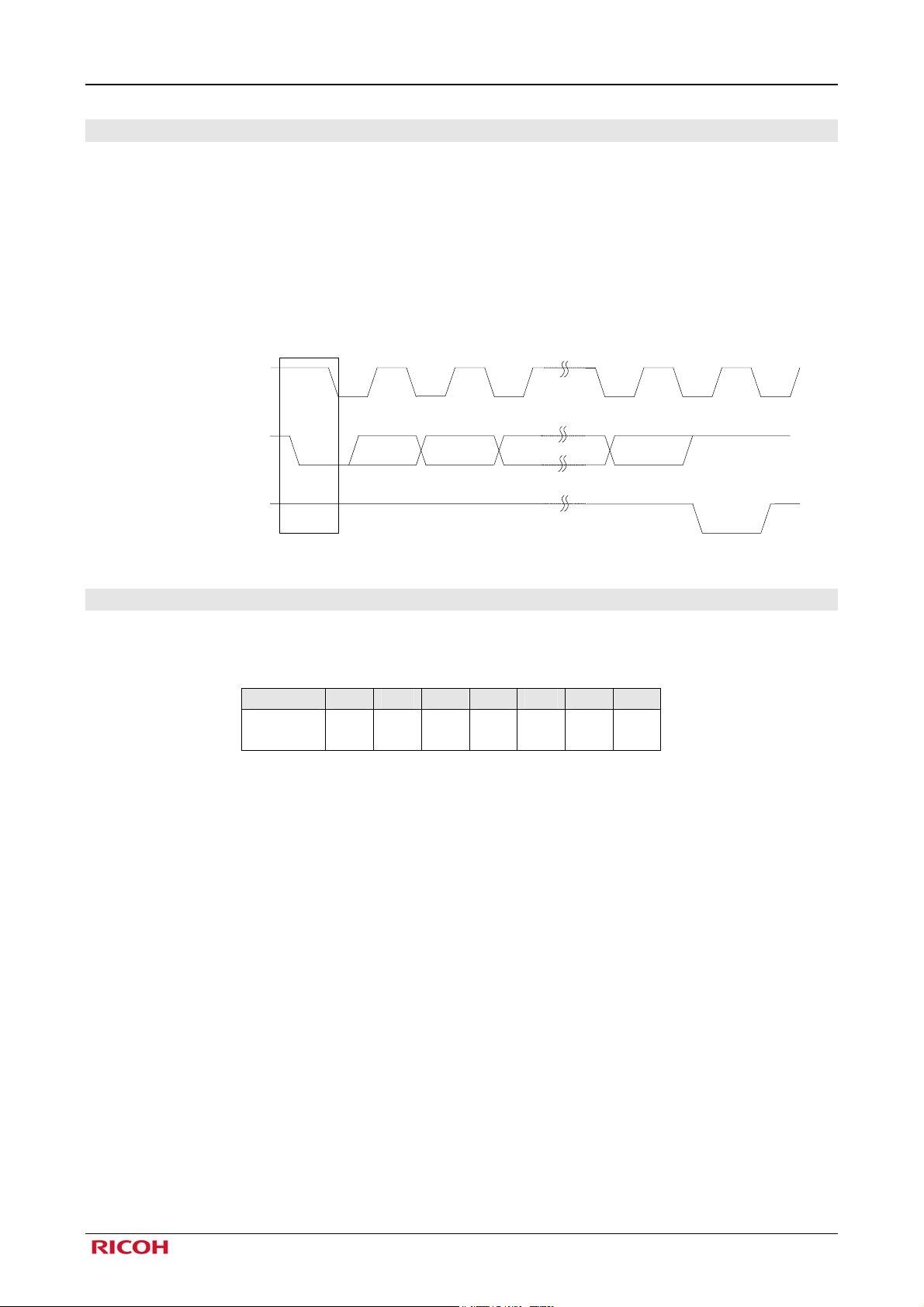
11. CPU Interface
RN5T614 uses I2C-Bus system for CPU connection through two wires. Connection and transfer system of I2C-Bus are
described in the following sections.
11.1 I2C-Bus Operation
Within the procedure of I2C-Bus, unique situations arise which are defined as Start and Stop conditions.
SCL
SDA
Fig 11-1 I2C-Bus Data Transmission
An “H” to “L” transition on SDA line while SCL is “H” indicates a Start condition. An “L” to “H” transition on SDA
line while SCL is “H” defines a Stop condition. Start and Stop conditions are always generated by master (refer to the
figure below). The bus is considered to be busy after Start condition. The bus is considered to be free again a certain
time after the stop condition.
SCL
SDA
Start Condition Stop Condition
Fig 11-2 I2C-Bus Start and Stop Condition
©2010-2011 Rev. 1.0 Page 38
RN5T614 POWER MANAGEMENT SYSTEM DEVICE
11.2 I2C-Bus Data Transmission and its Acknowledge
After start condition, data is transmitted by 1byte (8bits). The number of bytes that can be transmitted per transfer is
unrestricted. Each byte has to be followed by an acknowledge bit.
Data transmission with acknowledge is obligatory. The acknowledge-related clock pulse is generated by the master. The
transmitter releases SDA line during the acknowledge clock pulse.
The receiver must pull down SDA line during the acknowledge clock pulse so that SDA line remains stable “L” during
the “H” period of the acknowledge clock pulse.
If a master–receiver is involved in a transfer, it must signal the end of the data to the slave-transmitter by not generating
acknowledge on the last byte that was clocked out of the slave. The slave-transmitter must release the data line to allow
the master to generate a Stop condition.
SCL from
Master
SDA from
Transmitter
SDA from
Receiver
Start Condition
12 89
Acknowledge Signal
Fig 11-3 I2C-Bus Data Transmission and its Acknowledge
11.3 I2C-Bus Slave Address
After Start condition, a slave address is sent. The address is 7 bits long followed by an 8th bit which is data direction bit
(Read/Write). The slave address of RN5T614 is specified at “0110010b”.
A7 A6 A5 A4 A3 A2 A1
Setting
value
0 1 1 0 0 1 0
A7~A1: Slave Address
Table 11-1 Slave Address of RN5T614
©2010-2011 Rev. 1.0 Page 39

RN5T614 POWER MANAGEMENT SYSTEM DEVICE
11.4 I2C-Bus Data Transmission Read Format
In order to read the internal register data:
- Specify an internal address pointer (8bit).
- Generate the repeated Start condition to change the data transmission direction to read.
With a Start of read mode, automatic increment in address pointers will be made. Read-mode is repeated until Stop
condition is initiated.
R/W="0" (Write)
Repeated Start Condition
R/W="1"(Read)
0S 1 1 0 0 1 0 0 A A
Transmission of
Slave Address
(0011010)
Master to Slave
S Start Condition
P Stop Condition
Setting of Address to
the Internal Address
Pointer (n)
Reading of Data to the
Internal Address (n
Slave to Master AA Acknowledge Signal
Sr Repeated Start Condition
+1)h
AInternal Address (8bit)
Sr
0 1 1 0 0 1 0 1
Transmission of
Slave Address
(0011010)
Reading of Data to the
Internal Address (n
A
Reading of Data to the
Internal Address (n)h
....
ARead Data (8bit)ARead Data (8bit) Read Data (8bit)
Reading of Data to the
+2)h
Internal Address (n
+X)h
ARead Data (8bit)
P
A
Fig 11-4 I2C-Bus Data Transmission Read Format
11.5 I2C-Bus Data Transmission Write Format
The transmission format for the slave address allocated to each IC is defined by I2C-Bus standard. However
transmission method of address information of each IC is not defined. RN5T614 transmits command data. For the data
transmission, please transmit MSB first from Master and following data in sequence.
W="0"(Write)
0S 1 1 0 0 1 0 0 A AData
Transmission of
Slave Address
(01100100)
Master to Slave
S Start Condition
P Stop Condition
Setting of Address to the
Internal Address Pointer
(n)
Writing of Data to the
Internal Address (n
Slave to Master AAA Acknowledge Signal
+2)h
AData
Writing of Data to the
Internal Address (n)h
Writing of Data to the
Internal Address (n
Fig 11-5 I2C-Bus Data Transmission Write Format
Writing of Data to the
Internal Address (n
....
ADataAData AData
+3)h
AData
+1)h
Writing of Data to the
Internal Address (n
+X)h
P
©2010-2011 Rev. 1.0 Page 40
RN5T614 POWER MANAGEMENT SYSTEM DEVICE
11.6 I2C-Bus Internal Register Write-in Timing
SCL from Master
SDA from Master
SDA from Slave
Internal Register Write-in
Signal (WRB)
Start Condition
198765423
Fig 11-6 I2C-Bus Internal Register Write-in Timing
Acknowledge
Stop Condition
Writing to Internal Register
©2010-2011 Rev. 1.0 Page 41

RN5T614 POWER MANAGEMENT SYSTEM DEVICE
11.7 AC Characteristics of I2C-Bus
Operating Conditions (unless otherwise specified) VDDIO = 1.7~3.4V, Ta = 25 degrees C
Symbol Parameter Condition Min Typ Max Units
f
SCL Clock Frequency
SCL
t
BUF
t
Low
t
HIGH
t
SU;STA
t
HD;STA
t
SU;STO
t
HD;DAT
t
SU;DAT
tR
tF
Bus Free Time Between
a Precedent and Start
SCL Clock “L” Time
SCL Clock “H” Time
Start Condition Setup Time
Start Condition Hold Time
Stop Condition Setup Time
Data Hold Time
Data Setup Time
Rising Time of SCL and SDA (Input)
Falling Time of SCL and SDA (Input)
- 400 kHz
- 1.3 - μs
- 1.3 - μs
- 0.6 - μs
- 0.6 - μs
- 0.6 - μs
- 0.6 - μs
- 0 μs
- 100 (*1) - ns
- 300 ns
- 300 ns
Table 11-2 I2C-Bus AC Characteristics
Note*: All the above-mentioned values are corresponding to V
min and V
IH
max level.
IL
Note*1: Standard mode is allowed in I2C-bus standard. For Standard mode, it needs to satisfy the condition;
t
>=250ns.
SU;DAT
SDA
t
SCL
BUF
t
HD;STA
PS Sr P
t
LOW
t
R
t
HD;DAT
t
HIGHtF
t
SU;DAT
t
SU;STA
t
HD;STA
t
SU;STO
Fig 11-7 I2C-Bus Interface Timing Chart
©2010-2011 Rev. 1.0 Page 42
T
RN5T614 POWER MANAGEMENT SYSTEM DEVICE
12. Registers
Address Register R/W bit7 bit6 bit5 bit4 bit3 bit2 bit1 bit0
Power Contro l 00 PCCNT R/W --- --- --- --- --- --- --- SLEEP 0000 0000
DET 02 VDCTRL R/W --- --- --- 011* 0010
LDO 03 LDOON R/W --- LDO7ON LDO6ON LDO5ON LDO4ON LDO3ON LDO2ON --- 000* **10
06
07
08
09
0A
0B
DCDC 10 DDCTL1 R/W --- --- --- --- --- DD3ON DD2ON DD1ON 0000 0100
CHARGER 20 CHGSTART R/W --- --- --- --- --- --- --- CHGSTART 0000 0001
INTC 28 CHGEN1 R/W EN_VBOV EN_VCOV EN_NOBATT --- --- EN_VBTERR E N_DIEOT EN_ADPDET 0000 0001
01 PCST R --- --- --- --- --- --- EXTONMON PWRONMON 0000 00--
04 LDO2DAC R/W --- --- --- --- --- 0000 0011
05 LDO3DAC R/W --- --- --- --- --- 0000 0011
LDO4DAC R/W --- --- --- --- --- 0000 0110
LDO5DAC R/W --- --- --- --- --- 0000 0*0*
LDO6DAC R/W --- --- --- --- --- 0000 0011
LDO7DAC R/W --- --- --- --- --- 0000 0110
LDO8DAC R/W --- --- --- --- --- 0000 011*
0C --- --- --- --- --- --- --- --- --- --- ---- ---0D --- --- --- --- --- --- --- --- --- --- ---- ---0E --- --- --- --- --- --- --- --- --- --- ---- ----
1A --- --- --- --- --- --- --- --- --- --- ---- ----
1B
1C --- --- --- --- --- --- --- --- --- --- ---- ---1D --- --- --- --- --- --- --- --- --- --- ---- ---1E --- --- --- --- --- --- --- --- --- --- ---- ----
2A CHGMONI R MON_VBOV MON_VCOV MON_NOBAT
2B --- --- --- --- --- --- --- --- --- --- ---- ---2C CHGEN2 R/W --- --- --- EN_TIMEOUT EN_CHGCMP EN_STRC --- EN_STCR 0000 0000
2D CHGIR2 R/W --- --- --- IR_TIMEOUT IR_CHGCMP IR_STRC --- IR_STCR 0000 0000
2E --- --- --- --- --- --- --- --- --- --- ---- ----
--- --- --- --- --- --- --- --- --- --- ---- ----
0F --- --- --- --- --- --- --- --- --- --- ---- ----
11 DDCTL2 R/W --- --- --- --- --- --- DD2DIS DD1DIS 0000 0011
12 RAMP1CTL R/W --- --- DD1ENCTL --- 0001 1000
13 RAMP2CTL R/W --- --- DD2ENCTL --- 0001 1000
14 DD1DAC R/W --- 00** ***0
15 DD2DAC R/W --- 0*** **00
16 --- --- --- --- --- --- --- --- --- --- ---- ---17 --- --- --- --- --- --- --- --- --- --- ---- ---18 --- --- --- --- --- --- --- --- --- --- ---- ---19 --- --- --- --- --- --- --- --- --- --- ---- ----
--- --- --- --- --- --- --- --- --- --- ---- ----
1F --- --- --- --- --- --- --- --- --- --- ---- ----
21 FET1CNT R/W --- --- --- --- 0000 **0*
22 FET2CNT R/W --- --- 0000 **00
23 TSET R/W --- --- --- --- 0010 0000
24 CMPSET R/W --- --- --- --- --- 0000 0000
25 SUSPEND R/W --- --- --- CRCC2 --- --- --- SUSPENDB 0000 0001
26 CHGSTATE R --- --- --- --- 0000 0000
27 --- --- --- --- --- --- --- --- --- --- ---- ----
29 CHGIR1 R/W IR_VBOV IR_VCOV IR_NOBATT --- --- IR_VBTERR IR_DIEOT IR_ADPDET 0000 0000
2F --- --- --- --- --- --- --- --- --- --- ---- ----
VD2SEL[2:0]
LDO2DAC[2:0]
LDO3DAC[2:0]
LDO4DAC[2:0]
LDO5DAC[2:0]
LDO6DAC[2:0]
LDO7DAC[2:0]
LDO8DAC[2:0]
RAMP1SLOP[1:0] D D1MODE[1:0]
RAMP2SLOP[1:0] D D2MODE[1:0]
DD1DAC[6:0]
DD2DAC[6:0]
ILIM[3:0]
CVSET[1:0] ICHGSET[3:0]
TEMPSET[1:0] RTIMSET[1:0]
CMPSET[2:0]
RDSTATE[3:0]
--- --- MON_VBTERRMON_DIEOT MON_ADPDET---0 0---
VD1SEL[1:0]
Initial value
(*1)
Note*: Do not set "1" to reserved bits. Do not write "1" or "0" to undefined registers.
Note*1: Reset condition of register:
- PCCNT register (00h) and CHGIR1-2 registers (29h, 2Dh) are reset by UVLO or TSHUT.
- When VCHG power supply is turned off, CHARGER's registers (20h-26h) and CHGIR1-2 registers (29h, 2Dh) except IR_ADPDET bit are cleared.
- Other registers are reset by RESETO="L".
Also, when DC/DC1(2) turns off, DD1(2)MODE[1:0] bits and DD1(2)DAC[6:0] bits are reset.
"*" selected by trimming .
©2010-2011 Rev. 1.0 Page 43

RN5T614 POWER MANAGEMENT SYSTEM DEVICE
12.1 Power Control
12.1.1 PCCNT: Power Control Register (Address 00h)
Bit 7 6 5 4 3 2 1 0
Symbol - - - - - - - SLEEP
R/W R R R R R R R R/W
Default 0 0 0 0 0 0 0 0
Bit 0: SLEEP bit
12.1.2 PCST: Power Control Status Register (Address 01h)
“0”: Stand-by Operation is invalid
“1”: Stand-by Operation is valid
Note*: SLEEP bit is reset by UVLO or THSUT.
Bit 7 6 5 4 3 2 1 0
Symbol - - - - - - EXTON
MON
R/W R R R R R R R R
Default 0 0 0 0 0 0 - -
PWRON
MON
Bit 1: EXTON pin input monitor bit
“0”: EXTON=”L”
“1”: EXTON=”H”
Bit 0: PWRON pin input monitor bit
“0”: PWRON=”L”
“1”: PWRON=”H”
©2010-2011 Rev. 1.0 Page 44

RN5T614 POWER MANAGEMENT SYSTEM DEVICE
12.2 Voltage Detector
12.2.1 VDCTRL: Detection Circuit Control Register (Address 02h)
Bit 7 6 5 4 3 2 1 0
Symbol - VD2SEL[2:0] - - VD1SEL[1:0]
R/W R R/W R/W R/W R R R/W R/W
Default 0 1 1 1 0 0 1 0
Bit 6 ~ Bit 4: VD2SEL [2:0] bit
The release voltage setting of VD2
Bit 1 ~ Bit 0: VD1SEL[1:0] bit
The release voltage setting of VD1
The release voltage table of VD2
VD2SEL [2:0] Release voltage [V]
000 (0h) Prohibit
001 (1h) 1.53
010 (2h) 2.13
011 (3h) 2.21
100 (4h) 2.38
101 (5h) 2.42
110 (6h)
111 (7h) 2.81 (Default)
Note*: Initial value selected by trimming (2.55V or 2.81V)
Note*: Hysteresis of VD2 is 100mV.
The detection voltage is determined by this register setting.
The release voltage table of VD1
2.55
VD1SEL [1:0] Release voltage [V]
00 (0h) 3.1
01 (1h) 3.2
10 (2h)
3.3 (Default)
11 (3h) 3.5
Note*: Hysteresis of VD1 is 0.2V.
The detection voltage is determined by this register setting.
©2010-2011 Rev. 1.0 Page 45

RN5T614 POWER MANAGEMENT SYSTEM DEVICE
12.3 Regulator
12.3.1 LDOON: LDO Output Control Register (Address 03h)
Bit 7 6 5 4 3 2 1 0
Symbol - LDO7ON LDO6ON LDO5ON LDO4ON LDO3ON LDO2ON -
R/W R R/W R/W R/W R/W R/W R/W R
Default 0 0 0 1 1 1 1 0
Bit 7-1: LDOnON bit (n=2, 3, 4, 5, 6, 7)
LDOn on/off control bit
“0”: off
“1”: on
Note*: Initial value selected by trimming (LDO3, 4, 5)
12.3.2 LDO2DAC: LDO2 Output Voltage Control Register (Address 04h)
Bit 7 6 5 4 3 2 1 0
Symbol - - - - - LDO2DAC [2:0]
R/W R R R R R R/W R/W R/W
Default 0 0 0 0 0 0 1 1
Bit 2 ~ Bit 0: LDO2DAC [2:0] bit
Set the output voltage to LDO2
The output voltage table of LDO2
LDO2DAC [2:0] Output voltage [V]
000 (00h) 0.90
001 (01h) 1.00
010 (02h) 1.10
011 (03h)
1.20 (Default)
100 (04h) 1.30
101 (05h) Prohibit
110 (06h) Prohibit
111 (07h) Prohibit
©2010-2011 Rev. 1.0 Page 46

RN5T614 POWER MANAGEMENT SYSTEM DEVICE
12.3.3 LDO3DAC: LDO3 Output Voltage Control Register (Address 05h)
Bit 7 6 5 4 3 2 1 0
Symbol - - - - - LDO3DAC [2:0]
R/W R R R R R R/W R/W R/W
Default 0 0 0 0 0 0 1 1
Bit 2 ~ Bit 0: LDO3DAC [2:0] bit
Set the output voltage to LDO3
The output voltage table of LDO3
LDO3DAC [2:0] Output voltage [V]
000 (00h) 0.90
001 (01h) 1.00
010 (02h) 1.10
011 (03h)
1.20 (Default)
100 (04h) 1.30
101 (05h) Prohibit
110 (06h) Prohibit
111 (07h) Prohibit
12.3.4 LDO4DAC: LDO4 Output Voltage Control Register (Address 06h)
Bit 7 6 5 4 3 2 1 0
Symbol - - - - - LDO4DAC [2:0]
R/W R R R R R R/W R/W R/W
Default 0 0 0 0 0 1 1 0
Bit 2 ~ Bit 0: LDO4DAC [2:0] bit
Set the output voltage to LDO4
The output voltage table of LDO4
LDO4DAC [2:0] Output voltage [V]
000 (00h) 1.80
001 (01h) 2.50
010 (02h) 2.60
011 (03h) 2.80
100 (04h) 2.85
101 (05h) 3.00
110 (06h)
3.30 (Default)
111 (07h) Prohibit
©2010-2011 Rev. 1.0 Page 47
RN5T614 POWER MANAGEMENT SYSTEM DEVICE
12.3.5 LDO5DAC: LDO5 Output Voltage Control Register (Address 07h)
Bit 7 6 5 4 3 2 1 0
Symbol - - - - - LDO5DAC [2:0]
R/W R R R R R R/W R/W R/W
Default 0 0 0 0 0 0 0 0
Bit 2 ~ Bit 0: LDO5DAC [2:0] bit
Set the output voltage to LDO5
The output voltage table of LDO5
LDO5DAC [2:0] Output voltage [V]
000 (00h) 1.80 (Default)
001 (01h) 2.50
010 (02h) 2.60
011 (03h) 2.80
100 (04h) 2.85
101 (05h)
3.00
110 (06h) 3.30
111 (07h) Prohibit
Note*: Initial value selected by trimming (3.0V or 1.8V)
12.3.6 LDO6DAC: LDO6 Output Voltage Control Register (Address 08h)
Bit 7 6 5 4 3 2 1 0
Symbol - - - - - LDO6DAC [2:0]
R/W R R R R R R/W R/W R/W
Default 0 0 0 0 0 0 1 1
Bit 2 ~ Bit 0: LDO6DAC [2:0] bit
Set the output voltage to LDO6
The output voltage table of LDO6
LDO6DAC [2:0] Output voltage [V]
000 (00h) 1.20
001 (01h) 1.80
010 (02h) 2.50
011 (03h)
2.60 (Default)
100 (04h) 2.80
101 (05h) 2.85
110 (06h) 3.00
111 (07h) 3.30
©2010-2011 Rev. 1.0 Page 48

RN5T614 POWER MANAGEMENT SYSTEM DEVICE
12.3.7 LDO7DAC: LDO7 Output Voltage Control Register (Address 09h)
Bit 7 6 5 4 3 2 1 0
Symbol
R/W R R R R R R/W R/W R/W
Default 0 0 0 0 0 1 1 0
- - - - -
LDO7DAC [2:0]
Bit 2 ~ Bit 0: LDO7DAC [2:0] bit
Set the output voltage to LDO7
The output voltage table of LDO7
LDO7DAC [2:0] Output voltage [V]
000 (00h) 1.20
001 (01h) 1.80
010 (02h) 2.50
011 (03h) 2.60
100 (04h) 2.80
101 (05h) 2.85
110 (06h)
3.00 (Default)
111 (07h) 3.30
12.3.8 LDO8DAC: LDO8 Output Voltage Control Register (Address 0Ah)
Bit 7 6 5 4 3 2 1 0
Symbol - - - - - LDO8DAC [2:0]
R/W R R R R R R/W R/W R/W
Default 0 0 0 0 0 1 1 1
Bit 2 ~ Bit 0: LDO8DAC [2:0] bit
Set the output voltage to LDO8
The output voltage table of LDO8
LDO8DAC [2:0] Output voltage [V]
000 (00h) Prohibit
001 (01h) 1.80
010 (02h) 2.50
011 (03h) 2.60
100 (04h) 2.80
101 (05h) 2.85
110 (06h)
3.00
111 (07h) 3.30 (Default)
Note*: Initial value selected by trimming (3.0V or 3.3V)
©2010-2011 Rev. 1.0 Page 49

RN5T614 POWER MANAGEMENT SYSTEM DEVICE
12.3.9 DDCTL1: DC/DC Control Register1 (Address 10h)
Bit 7 6 5 4 3 2 1 0
Symbol - - - - - DD3ON DD2ON DD1ON
R/W R R R R R R/W R/W R/W
Default 0 0 0 0 0 1 0 0
Bit 2-0: DDnON bit (n=1,2,3)
DC/DCn on/off bit
“0”: off
“1”: on
12.3.10 DDCTL2: DC/DC Control Register2 (Address 11h)
Bit 7 6 5 4 3 2 1 0
Symbol - - - - - - DD2DIS DD1DIS
R/W R R R R R R R/W R/W
Default 0 0 0 0 0 0 1 1
Bit 2-0: DDnDIS bit (n=1, 2)
DC/DCn Discharge control bit
“0”: off
“1”: on (This bit is invalid when DC/DCn state is on.)
DC/DCnOFF
(Internal Signal)
DDnDIS bit
Discharge Tr
GND
©2010-2011 Rev. 1.0 Page 50

RN5T614 POWER MANAGEMENT SYSTEM DEVICE
12.3.11 RAMP1CTL: DC/DC1 RAMP Control Register (Address 12h)
Bit 7 6 5 4 3 2 1 0
Symbol - - RAMP1SLOP [1:0] DD1MODE [1:0] DD1ENCTL -
R/W R R R/W R/W R/W R/W R/W R
Default 0 0 0 1 1 0 0 0
Bit 5-4: RAMP1SLOP [1:0] bit
DC/DC1 RAMP up/down slope setting bit
RAMP1SLOP[1:0] Voltage Slope
00 15 mV /μs
01 30 mV /μs (Default)
10 60 mV /μs
11 Prohibit
Bit 3-2: DD1MODE bit
DC/DC1 AUTO(PWM/PFM) / PWM / PSM mode setting bit
DD1MODE [1:0] Operation Mode
00 PSM
01 PWM
10 AUTO (Default)
11 AUTO
DD1MODE bit is reset when DC/DC1 turns off and changed to AUTO mode.
Bit 1: DD1ENCTL bit
DC/DC1 Control select bit
“0”: DCDCEN12 pin is valid
“1”: DD1ON bit is valid
©2010-2011 Rev. 1.0 Page 51

RN5T614 POWER MANAGEMENT SYSTEM DEVICE
12.3.12 RAMP2CTL: DC/DC2 RAMP Control Register (Address 13h)
Bit 7 6 5 4 3 2 1 0
Symbol - - RAMP2SLOP [1:0] DD2MODE [1:0] DD2ENCTL -
R/W R R R/W R/W R/W R/W R/W R
Default 0 0 0 1 1 0 0 0
Bit 5-4: RAMP2SLOP [1:0] bit
DC/DC2 RAMP up/down slope setting bit
RAMP2SLOP[1:0] Voltage Slope
00 15 mV /μs
01 30 mV /μs (Default)
10 60 mV /μs
11 Prohibit
Bit 3-2: DD2MODE bit
DC/DC2 AUTO(PWM/PFM)/PWM / PSM mode setting bit
DD2MODE [1:0] Operation Mode
00 PSM
01 PWM
10 AUTO (Default)
11 AUTO
DD2MODE bit is reset when DC/DC2 turns off and changed to AUTO mode.
Bit 1: DD2ENCTL bit
DC/DC2 Control select bit
“0”: DCDCEN12 pin is valid
“1”: DD2ON bit is valid
©2010-2011 Rev. 1.0 Page 52
RN5T614 POWER MANAGEMENT SYSTEM DEVICE
12.3.13 DD1DAC: DC/DC1 Output Voltage Control Register (Address 14h)
DD1DAC (14h)
Bit 7 6 5 4 3 2 1 0
Symbol - DD1DAC [6:0]
R/W R R/W R/W R/W R/W R/W R/W R/W
Default 0 0 0 1 1 0 0 0
Note*: The register value is reset when DC/DC1 turns off. (Initial value selected by trimming)
The output voltage table of DC/DC1 (Step=12.5mV)
DD1DAC [6:0] Output voltage [V]
0000000 (00h) 0.9000
0000001 (01h) 0.9125
0000010 (02h) 0.9250
~ ~
0001000 (08h) 1.00
~ ~
0010000 (10h) 1.10
~ ~
0011000 (18h) 1.20 (Default)
~ ~
0011100 (1Ch) 1.25
~ ~
0100000 (20h) 1.3
~ ~
0101010 (2Ah) 1.4250
~ ~
0101110 (2Eh) 1.4750
0101111 (2Fh) 1.4875
0110000 (30h) 1.5000
~
Prohibit
1111111 (7Fh) Prohibit
©2010-2011 Rev. 1.0 Page 53

RN5T614 POWER MANAGEMENT SYSTEM DEVICE
12.3.14 DD2DAC: DC/DC2 Output Voltage Control Register (Address 15h)
DD2DAC (15h)
Bit 7 6 5 4 3 2 1 0
Symbol - DD2DAC [6:0]
R/W R R/W R/W R/W R/W R/W R/W R/W
Default 0 0 0 1 0 1 0 0
Note*: The register value is reset when DC/DC2 turns off. (Initial value selected by trimming)
The output voltage table of DC/DC2 (Step=12.5mV)
DD2DAC [6:0] Output voltage [V]
0000000 (00h) 0.9000
0000001 (01h) 0.9125
0000010 (02h) 0.9250
~ ~
0000100 (04h) 0.95
~ ~
0001100 (0Ch) 1.05
~ ~
0010100 (14h) 1.15 (Default)
~ ~
0011000 (18h) 1.20
~ ~
0101110 (2Eh) 1.4750
0101111 (2Fh) 1.4875
0110000 (30h) 1.5000
~
Prohibit
1001000 (48h) 1.8
~
Prohibit
1111111 (7Fh) Prohibit
©2010-2011 Rev. 1.0 Page 54
RN5T614 POWER MANAGEMENT SYSTEM DEVICE
12.4 Li-ion Battery Charger
12.4.1 CHGSTART: Charging Start Setting Register (Address 20h)
Bit 7 6 5 4 3 2 1 0
Symbol - - - - - - - CHGSTART
R/W
Default
Bit 0: CHGSTART bit
Battery Charging enables
“0”: Disable charging
“1”: Enable charging (default)
12.4.2 FET1CNT: SW1 Limit Current Setting Register (Address 21h)
R R R R R R R
0 0 0 0 0 0 0
R/W
1
Bit 7 6 5 4 3 2 1 0
Symbol - - - - ILIM[3:0]
R/W
Default
R R R R
0 0 0 0
R/W R/W R/W R/W
0 1 0 1
Bit 3 ~ Bit 0: ILIM bit
SW1 Limit Current Selection
Control Bit
SW1 Limit Current [mA]
D3 D2 D1 D0
0 0 0 0 120
0 0 0 1 240
0 0 1 0 360
0 0 1 1 480
0 1 0 0 600
0 1 0 1 720 (default)
0 1 1 0 840
0 1 1 1 960
1 0
0
0 1080
other 1200
Note*: Initial value selected by trimming (120mA or 720mA or 1200mA)
©2010-2011 Rev. 1.0 Page 55

RN5T614 POWER MANAGEMENT SYSTEM DEVICE
12.4.3 FET2CNT: SW2 Control Setting Register (Address 22h)
Bit 7 6 5 4 3 2 1 0
Symbol - CVSET[1:0] - ICHGSET[3:0]
R/W R R/W R/W R R/W R/W R/W R/W
Default 0 0 0 0 0 1 0 0
Bit 6 ~ Bit 5: CVSET bit
Battery Charge Voltage Selection
Control Bit
Charge voltage [V]
D1 D0
0 0 4.2 (default)
0 1 4.12
1 0 4.07
1 1 4.07
Bit 3 ~ Bit 0: ICHGSET bit
Rapid Current Selection
Control Bit
Rapid Current [mA]
D3 D2 D1 D0
0 0 0 0 100
0 0 0 1 200
0 0 1 0 300
0 0 1 1 400
0 1 0 0 500 (default)
0 1 0 1 600
0 1 1 0 700
0 1 1 1 800
other 900
Note*: Initial value selected by trimming (100mA or 500mA or 900mA)
©2010-2011 Rev. 1.0 Page 56

RN5T614 POWER MANAGEMENT SYSTEM DEVICE
12.4.4 TSET: Temperature and Charging Timer Setting Register (Address 23h)
Bit 7 6 5 4 3 2 1 0
Symbol
R/W
Default
- - TEMPSET[1:0]
R R R/W R/W R R R R
0 0 1 0 0 0 0 0
RTIMSET[1:0] - -
Bit 5 ~ Bit 4: TEMPSET bit
Die over temperature threshold value selection
Control Bit Die Temperature [degrees C]
D5 D4 Detection Recovery
0 0 105 85
0 1 115 95
1 0
125 (default)
105
1 1 135 115
Bit 3 ~ Bit 2: RTIMSET bit
Rapid Timer setting
Control Bit
Rapid Timer [min]
D3 D2
0 0 120 (default)
0 1 180
1 0 240
1 1 300
©2010-2011 Rev. 1.0 Page 57
RN5T614 POWER MANAGEMENT SYSTEM DEVICE
12.4.5 CMPSET: Charge Complete Current Setting Register (Address 24h)
Bit 7 6 5 4 3 2 1 0
Symbol
R/W
Default
- - - -
R R R R R R/W R/W R/W
0 0 0 0 0 0 0 0
- CMPSET[2:0]
Bit 2 ~ Bit 0: CMPSET bit
Charge complete Current selection
Control Bit
D2 D1 D0
Charge Complete
Current [mA]
0 0 0 25 (default)
0 0 1 50
0 1 0 75
0 1 1 100
1 0 0 125
1 0 1 150
1 1 0 175
1 1 1 200
12.4.6 SUSPEND: Charge Ready Current / Suspend Setting Register (Address 25h)
Bit 7 6 5 4 3 2 1 0
Symbol
R/W
Default
- - - CRCC2
R R R R/W R R R R/W
0 0 0 0 0 0 0 1
- - - SUSPENDB
Bit 4: CRCC2 bit
Charge Ready Current Selection
“0”: 0mA (default)
“1”: 10mA
In Charge-Ready state, if the power source switches from the adapter to the battery, the transient under-shoot
might appear on VSYS pin because SW2 is fully off.
This under-shoot is able to be reduced by setting “1” to CRCC2 as SW2 is on even in Charge-Ready state.
Bit 0: SUSPENDB bit
Suspend Selection
“0”: Suspend
“1”: Not suspend (default)
(This bit is automatically set depending on the charge state).
SUSPENDB bit is set to “1” automatically and unable to set to “0” except when the state is Charge-Off,
Adapter-Over-Voltage, SUSPEND, Charge-Ready, Trickle-Charge, Rapid-Charge and Charge-Complete.
©2010-2011 Rev. 1.0 Page 58
RN5T614 POWER MANAGEMENT SYSTEM DEVICE
12.4.7 CHGSTATE: Current Charger State Register (Address 26h)
Bit 7 6 5 4 3 2 1 0
Symbol - - - - RDSTATE[3:0]
R/W R R R R R R R R
Default 0 0 0 0 0 0 0 0
Bit 0 ~ Bit 3: RDSTATE bit
Charger current state (read only)
Control Bit
Charger current state
D3 D2 D1 D0
0 0 0 0 Charge-Off
0 0 0 1 Charge-Ready
0 0 1 0 -
0 0 1 1 -
0 1 0 0 Rapid-Charge
0 1 0 1 Charge-Complete
0 1 1 0 Battery-Error
0 1 1 1 Battery-Over-Voltage
1 0 0 0 Adapter-Over-Voltage
1 0 0 1 No-Battery
1 0 1 0 Battery-Temperature-Error
1 0 1 1 SUSPEND
other -
©2010-2011 Rev. 1.0 Page 59

RN5T614 POWER MANAGEMENT SYSTEM DEVICE
12.5 Interrupt Controller
12.5.1 CHGEN1: Charge Interrupt Request Output Enable Register (Address 28h)
Bit 7 6 5 4 3 2 1 0
Symbol
R/W R/W R/W R/W R R R/W R/W R/W
Default 0 0 0 0 0 0 0 1
EN_VBOV EN_VCOV EN_NOBATT -
Bit 7: EN_VBOV bit
Battery over voltage interrupt enable (VVBAT > 4.6V)
“0”: Disable
“1”: Enable
Bit 6: EN_VCOV bit
Adapter over voltage interrupt enable (VVCHG>6.2V)
“0”: Disable
“1”: Enable
Bit 5: EN_NOBATT bit
No Battery detect interrupt enable
“0”: Disable
“1”: Enable
Bit 2: EN_VBTERR bit
Battery abnormal temperature interrupt enable
“0”: Disable
“1”: Enable
Bit 1: EN_DIEOT bit
Die abnormal temperature by SW1 or SW2 in charger interrupt enable
“0”: Disable
“1”: Enable
Bit 0: EN_ADPDET bit
Adapter insert & remove interrupt enable
“0”: Disable
“1”: Enable
-
EN_VBTERR EN_DIEOT EN_ADPDET
©2010-2011 Rev. 1.0 Page 60

RN5T614 POWER MANAGEMENT SYSTEM DEVICE
12.5.2 CHGIR1: Charge Interrupt Request Register (Address 29h)
Bit 7 6 5 4 3 2 1 0
Symbol
R/W R/W R/W R/W R R R/W R/W R/W
Default
IR_VBOV IR_VCOV IR_NOBATT -
0 0 0 0
-
0
IR_VBTERR IR_DIEOT
0 0
IR_ADPDET
Bit 7: IR_VBOV bit
Battery over voltage (VVBAT > 4.6V)
“0”: None
“1”: Requested
Bit 6: IR_VCOV bit
Adapter over voltage (VVCHG>6.2V)
“0”: None
“1”: Requested
Bit 5: IR_NOBATT bit
No Battery detect
“0”: None
“1”: Requested
Bit 2: IR_VBTERR bit
Battery abnormal temperature
“0”: None
“1”: Requested
Bit 1: IR_DIEOT bit
Die abnormal temperature by SW1 or SW2 in charger
“0”: None
“1”: Requested
Bit 0: IR_ADPDET bit
Adapter insert & remove
“0”: None
“1”: Requested
Note*: Each bit can be cleared by writing “0”, but cannot be set by writing “1”.
These bits are not cleared by RESETO=“L”.
These bits are cleared by UVLO or TSHUT.
Also, these bits are cleared when VCHG power supply is turned off.
0
©2010-2011 Rev. 1.0 Page 61
RN5T614 POWER MANAGEMENT SYSTEM DEVICE
12.5.3 CHGMONI: Charge Interrupt Monitor Signal Read Register (Address 2Ah)
Bit 7 6 5 4 3 2 1 0
Symbol MON_
VBOV
R/W R R R R R
Default - - - 0 0
MON_
VCOV
MON_
NOBATT
- - MON_
VBTERR
R R R
- - -
MON_
DIEOT
Bit 7: MON_VBOV bit
Battery over voltage (VVBAT > 4.6V) (Read Current Value)
“0”: Normal voltage
“1”: Over voltage
Bit 6: MON_VCOV bit
Adapter over voltage (VVCHG>6.2V) (Read Current Value)
“0”: Normal voltage
“1”: Over voltage
Bit 5: MON_NOBATT bit
No Battery detect (Read Current Value)
“0”: Battery is connected
“1”: Battery has come off
Bit 2: MON_VBTERR bit
Battery abnormal temperature (Read Current Value)
“0”: Normal temperature
“1”: Abnormal temperature
Bit 1: MON_DIEOT bit
Die abnormal temperature by SW1 or SW2 in charger (Read Current Value)
“0”: Normal temperature
“1”: Abnormal temperature
Bit 0: MON_ADPDET bit
Adapter insert & remove (Read Current Value)
“0”: Adapter has come off
“1”: Adapter is connected
MON_
ADPDET
©2010-2011 Rev. 1.0 Page 62
RN5T614 POWER MANAGEMENT SYSTEM DEVICE
12.5.4 CHGEN2: Charge Interrupt Request Output Enable Register (Address 2Ch)
Bit 7 6 5 4 3 2 1 0
Symbol - - -
R/W R R R R/W R/W R/W R R/W
Default 0 0 0 0 0 0 0 0
EN_TIMEOUT EN_CHGCMP EN_STRC
-
EN_STCR
Bit 4: EN_TIMEOUT bit
Timer time out interrupt enable
“0”: Disable
“1”: Enable
Bit 3: EN_CHGCMP bit
Charge complete interrupt enable
“0”: Disable
“1”: Enable
Bit 2: EN_STRC bit
Shift to Rapid-Charge state interrupt enable
“0”: Disable
“1”: Enable
Bit 0: EN_STCR bit
Shift to Charge-Ready state interrupt enable
“0”: Disable
“1”: Enable
©2010-2011 Rev. 1.0 Page 63

RN5T614 POWER MANAGEMENT SYSTEM DEVICE
12.5.5 CHGIR2: Charge Interrupt Request Register (Address 2Dh)
Bit 7 6 5 4 3 2 1 0
Symbol - - -
R/W R R R R/W R/W R/W R R/W
Default 0 0 0 0 0 0 0 0
IR_TIMEOUT IR_CHGCMP IR_STRC
-
IR_STCR
Bit 4: IR_TIMEOUT bit
Timer time out
“0”: None
“1”: Requested
Bit 3: IR_CHGCMP bit
Charge complete
“0”: None
“1”: Requested
Bit 2: IR_STRC bit
Shift to Rapid-Charge state
“0”: None
“1”: Requested
Bit 0: IR_STCR bit
Shift to Charge-Ready state
“0”: None
“1”: Requested
Note*: Each bit can be cleared by writing “0”, but cannot be set by writing “1”.
These bits are not cleared by RESETO=“L”.
These bits are cleared by UVLO or TSHUT.
Also, these bits are cleared when VCHG power supply is turned off.
©2010-2011 Rev. 1.0 Page 64

RN5T614 POWER MANAGEMENT SYSTEM DEVICE
13. Electrical Characteristics
13.1 Absolute Maximum Ratings
Exposure to the condition exceeded Absolute Maximum Ratings may cause the permanent damages and affects the
reliability and safety of both device and systems using the device. The functional operations cannot be guaranteed
beyond specified values in the recommended conditions.
VDD=V
Symbol Parameter Condition Rated value Units
VIN Power Supply Voltage VIN1-3 pins -0.3~6.0 V
V
Power Supply Voltage VSYS1-2 pins -0.3~6.0 V
VSYS
V
Power Supply Voltage VCHG1-2 Pins -0.3~6.5 V
VCHG
V
Power Supply Voltage VDDIO pin -0.3~4.5 V
DDIO
Vin Input Voltage Range All Input Pins -0.3~VDD+0.3 V
Vout Output Voltage Range -0.3~VDD+0.3 V
JEDEC substrate mounting state,
PD
T
Storage Temperature - -55~+125 degrees C
stg
Tj Junction Temperature 125 degrees C
Package
Allowable Dissipation
Wind velocity 0m/s Ta=25degrees C
Linear derating coefficient
= 0.03 W/ degrees C
3.0 W
, V
DDIO
IN
Table 13-1 Absolute Maximum Ratings
PD[W]
3.0
Linear derating coefficient
=0.03 [W/degrees C]
1.2
25 85 125 degrees C
Fig 13-1 Maximum Package Allowable Dissipation
13.2 Recommendation of Operating Conditions
Symbol Parameter Condition Min Ty p Max Units
VIN Power Supply Voltage VIN1-3 pins 3.1 3.6 5.5 V
V
Power Supply Voltage VSYS1-2 pins
VSYS
V
Power Supply Voltage VCHG1-2 Pins 4.5 5.0 5.5 V
VCHG
V
Power Supply Voltage VDDIO pin 1.7 3.4 V
DDIO
Ta Temperature of Operation - -40 +85 degrees C
4.65 4.8 4.95
V
Table 13-2 Recommendation of Operation Conditions
©2010-2011 Rev. 1.0 Page 65
RN5T614 POWER MANAGEMENT SYSTEM DEVICE
13.3 DC Characteristics
Digital part I/O
Operating Conditions (unless otherwise specified) T
Symbol Parameter Condition Min Ty p Max Units
VIH
V
V
V
V
V
V
V
V
VIL
HIS1
HIS2
OL1
OL2
IIL
IOZ
“H” input voltage (CMOS)
“L” input voltage (CMOS)
“H” input rising threshold
IH1
voltage1 (CMOS Schmitt)
“L” input rising threshold
IL1
voltage1 (CMOS Schmitt)
Schmitt hysteresis voltage1
“H” input rising threshold
IH2
voltage2 (CMOS Schmitt)
“L” input rising threshold
IL2
voltage2 (CMOS Schmitt)
Schmitt hysteresis voltage2
(SCL, SDA)
“L” Output Voltage1
“L” Output Voltage2
Input Leakage Current
Off Leakage Current
(SDA)
Pin=DCDCEN12, DCDCEN3
Pin=DCDCEN12, DCDCEN3
Pin=PWRON,EXTON,PSHOLD
Pin=PWRON,EXTON, PSHOLD
Pin=PWRON,EXTON, PSHOLD
Pin=SCL, SDA
Pin=SCL, SDA
VDD>2.0V
VDD<2.0V
I
Pin=ONOB, BATDET, RESETO, INTB
IOL= 3mA
I
VIN=0~VDD
VIN=0~VDD,
Pin=ONOB, BATDET, RESETO, INTB
= 25 degrees C, VDD = VIN/V
a
= 2mA,
OL
= 6mA
OL
DDIO
VDD×0.7 V
VDD×0.3 V
VDD×0.5 VDD×0.8 V
VDD×0.2 VDD×0.5 V
VDD×0.15 V
VDD×0.7 V
VDD×0.3 V
VDD×0.05
VDD×0.1
0.4 V
0.4 V
0.6 V
-3 3 μA
-3 3 μA
V
Table 13-3 DC Characteristics
Consumption Current
Operating Conditions (unless otherwise specified) T
Symbol Parameter Condition Min Ty p Max Units
I
ST1
I
ST2
IOP
Standby current1
Standby current2
Operating
current1
(UVLO,VD1,LDO1,LDODIG=ON)
(UVLO,VD1,2,VREF,LDO1,LDODIG,DCDC3,TSHUT=ON)
Not powered – on
powered – on (Standby mode)
powered – on (Normal mode)
(LDO,DC/DC = all ON)
= 25 degrees C, VIN =3.6V, No-load
a
5 μA
100
320
Table 13-4 Consumption Current
μA
μA
©2010-2011 Rev. 1.0 Page 66

RN5T614 POWER MANAGEMENT SYSTEM DEVICE
14. Appendix
◎External Components
VDDIO
OVPAdapter
(1608/6.3V)
Li-ion
Battery
NTCG103JF103GT
(TDK)
10 kΩ±1%
HOST
Interface
4.7 uF
4.7 uF
(2012/10V)
10 kΩ
1.0 uF
10 uF
(1608/6.3V)
1.0 uF
1.0 uF
1.0 uF
1.0 uF
2.2 uF
(1608/6.3V)
2.2 uF
(1608/6.3V)
2.2 uF
(1608/6.3V)
0.1 uF
VCHG
VBAT1
VBAT2
THERMBAT
IMONI
VCHGREG
CHGLED
VOUT1
VTHM
VOUT2
VSYS1
VOUT3
VSYS2
VSYS3
VIN1
VIN2
RN5T614
VOUT4
VOUT5
VOUT6
VIN3 VOUT7
VINA
VINP1
VOUT8
VREF
VOUTD
VINP2
VINP3
VDDIO
DCDCEN12
LX1
VFB1
LX2
VFB2
DCDCEN3
PSHOLD
SCL
VDDIO level
Interface
LX3
VFB3
SDA
PWRON
EXTON
TEST1
TEST2
VDDIO level
Interface
INTB
BATDET
ONOB
RESETO
1kΩ
1.0 uF
1.0 uF
1.0 uF
1.0 uF
1.0 uF
1.0 uF
1.0 uF
1.0 uF
1.0 uF
1.0 uF
1.0 uF
2.2 uH
2.2 uH
2.2 uH
VSYS
10 uF
10 uF
CfR14.7 uF
R2
HOST
Interface
GND
©2010-2011 Rev. 1.0 Page 67

RN5T614 POWER MANAGEMENT SYSTEM DEVICE
◎Selectable by Trimming(Sequence1~4)
・Sequence1
VIN*
VOUT1
PWRON
(or EXTON)
(or Charging)
PSHOLD
VREF
DCDC3
VOUT8
VOUT5
VOUT3
VOUT4
VOUT2
UVLO
Power-on by PWRON(or EXTON or Charging)
0.5ms
12clk
12clk
4clk
4clk
4clk
Power-on by PWRON
(or EXTON or Charging)
0.2ms or more
Holding Power-on
by PSHOLD
2ms (invalid)
(valid)
(invalid)
DCDCEN12
from AP
DCDC1/2
The power needs to be supplied to VDDIO.
LDO6,7
RESETO
120ms
I2C Enabled
Note*: Internal clk (32kHz±20%)
Note*: The trimming setting of this sequence:
- DCDCEN12 pin is valid 2ms after the start of power-on. DCDCEN3 pin is invalid.
- LDO2 and VREF turn on following the power-on sequence.
- Default of LDOnON bit is “on”. (n=3, 4, 5)
- Power-on by Charging is valid.
(Initial value of ILIM[3:0] bits is 720mA.)
(Initial value of ICHGSET[3:0] bits is 500mA.)
©2010-2011 Rev. 1.0 Page 68

RN5T614 POWER MANAGEMENT SYSTEM DEVICE
・Sequence2
VIN*
VOUT1
PWRON
(or EXTON)
(or Charging)
PSHOLD
VREF
DCDC3
VOUT8
VOUT5
VOUT3
VOUT4
VOUT2
UVLO
Power-on by PWRON(or EXTON or Charging)
Holding Power-on by PSHOLD
0.2ms or more
0.5ms
12clk
12clk
4clk
4clk
4clk
(invalid)
(valid)
DCDCEN12
from AP
8clk
DCDC1/2
LDO6,7
RESETO
120ms
Note*: Internal clk (32kHz±20%)
I2C Enabled
Note*: The trimming setting of this sequence:
- DCDCEN12 pin is valid after RESETO is released. DCDCEN3 pin is invalid.
- LDO2 and VREF turn on following the power-on sequence.
- Default of LDOnON bit is “on”. (n=3, 4, 5)
- Power-on by Charging is valid.
(Initial value of ILIM[3:0] bits is 720mA.)
(Initial value of ICHGSET[3:0] bits is 500mA.)
(invalid)
©2010-2011 Rev. 1.0 Page 69

RN5T614 POWER MANAGEMENT SYSTEM DEVICE
・Sequence3
VIN*
VOUT1
PWRON
(or EXTON)
(or Charging)
PSHOLD
VREF
DCDC3
VOUT4
VOUT8
VOUT5
VOUT3
VOUT2
UVLO
Power-on by PWRON(or EXTON or Charging)
Holding Power-on by PSHOLD
0.2ms or more
4clk
8clk
0.5ms+12clk
12clk
4clk
8clk
(invalid)
(valid)
DCDCEN12
from AP
DCDC1/2
0.5ms+8clk
LDO6,7
RESETO
120ms
Note*: Internal clk (32kHz±20%)
I2C Enabled
Note*: The trimming setting of this sequence:
- DCDCEN12 pin is valid after RESETO is released. DCDCEN3 pin is invalid.
- LDO2 and VREF turn on following the power-on sequence.
- Default of LDOnON bit is “on”. (n=3, 4, 5)
- Power-on by Charging is valid.
(Initial value of ILIM[3:0] bits is 1200mA.)
(Initial value of ICHGSET[3:0] bits is 900mA.)
(invalid)
©2010-2011 Rev. 1.0 Page 70

RN5T614 POWER MANAGEMENT SYSTEM DEVICE
・Sequence4
VIN*
UVLO
VOUT1,2
VREF
Power-on by PWRON(or EXTON)
Holding Power-on by PSHOLD
PWRON
(or EXTON)
0.2ms or more
PSHOLD
(valid)
0.5ms
DCDC3
12clk
VOUT8
DCDCEN12
(invalid)
(valid) (invalid)
DCDCEN3
from AP
8clk
DCDC1/2
LDO3,4,5,6,7
RESETO
Note*: Internal clk (32kHz±20%)
120ms
I2C Enabled
Note*: The trimming setting of this sequence:
- DCDCEN12 pin and DCDCEN3 pin are valid after RESETO is released.
- LDO2 and VREF are always on.
- Default of LDOnON bit is “off”. (n=3, 4, 5)
- Power-on by Charging is invalid.
(Initial value of ILIM[3:0] bits is 720mA.)
(Initial value of ICHGSET[3:0] bits is 500mA.)
©2010-2011 Rev. 1.0 Page 71
 Loading...