


7-channel Power Management IC
RN5T564
Development Specifications
Rev. 1.4
2009.06.25
RICOH COMPANY, LTD.
Electronic Devices Company
This specification is subject to change without notice.

RN5T564 7-channel Power Management IC
Table of Contents
1. Outline..................................................................................................................................................... 3
2. Feature .................................................................................................................................................... 3
3. Pin Configuration .................................................................................................................................... 4
4. Block diagram.......................................................................................................................................... 5
5. Pin Description ........................................................................................................................................ 6
6. Power ON/OFF Operation ....................................................................................................................... 7
6.1 Power ON/OFF Operation ..................................................................................................................................7
6.2 UVLO (Under Voltage Lock Out) Electrical Characteristics .............................................................................8
6.3 Thermal Shutdown Circuit Electrical Characteristics .........................................................................................8
7. Reset Function ............................................................................................................................... ..........9
8. FUNCTION Blocks ................................................................................................................................10
8.1 LDO, DCDC Table ...........................................................................................................................................10
8.2 LDO ..................................................................................................................................................................11
8.2.1 LDO1, 2, 3 Electrical Characteristics ...................................................................................................... 12
8.2.2 LDO4, 5 Electrical Characteristics .......................................................................................................... 13
8.3 Step-down DC/DC Converter...........................................................................................................................14
8.3.1 Step-down DC/DC Converter1 Electrical Characteristics ....................................................................... 14
8.3.2 Step-down DC/DC Converter2 Electrical Characteristics ....................................................................... 15
8.3.3 Step-down DC/DC Converter2 Output Voltage Setting........................................................................... 16
9. CPU Interface ........................................................................................................................................ 17
9.1 I2C BUS............................................................................................................................................................17
9.1.1 Method of I2C-Bus Transfer.................................................................................................................... 17
9.1.2 I2C-Bus Slave Address ............................................................................................................................ 18
9.1.3 I2C-Bus Data Transmission Format ........................................................................................................19
9.1.4 I2C-Bus SDA and SCL Bus Line characteristics..................................................................................... 21
10. Register.................................................................................................................................................. 23
10.1 Register Map.....................................................................................................................................................23
10.2 Register Description..........................................................................................................................................24
10.2.1 PWRON Register (Address: 00h)............................................................................................................ 24
©2009 Rev. 1.4 Page 1

RN5T564 7-channel Power Management IC
10.2.2 MODE Register (Address: 01h) ..............................................................................................................24
10.2.3 LDO Setting Voltage Register (Address: 02h)......................................................................................... 25
11. Electrical Characteristics .......................................................................................................................26
11.1 Absolute Maximum Ratings .............................................................................................................................26
11.2 Recommendation of Operation Conditions.......................................................................................................26
11.3 System Consumption Current ...........................................................................................................................26
12. Electrical Characteristics of Digital Input/Output Pin............................................................................ 27
12.1 VDD system CMOS Schmitt Input Pin.............................................................................................................27
12.2 VDD system Nch Open Drain Output Pin ........................................................................................................27
12.3 VIND system CMOS Schmitt Input Pin ...........................................................................................................27
12.4 VDD system CMOS Input pin..........................................................................................................................27
12.5 VIND system NchOpen Drain Output Pin........................................................................................................27
13. Package Information.............................................................................................................................. 28
©2009 Rev. 1.4 Page 2

RN5T564 7-CHANNEL POWER MANAGEMENT IC
1. Outline
RN5T564 is the power management IC for GPS. It integrates 2 high-efficiency Step-down DCDC controllers,
5 Low dropout regulators, Power control logic, Reset Detection, I2C interface and etc.
2. Feature
● High Efficiency Synchronous Step-down DCDC Converters
・DC/DC1 0.9 to 1.6V by trimming @ 500mA (for Core) PWM/VFM mode
・DC/DC2 0.9 to 3.3V by external resistor @ 500mA (for Memory)
* When DCDC1 is OFF, DCDC2 must not be loaded the current of 50mA or more
● Low Drop Voltage Regulator
・LDO1,LDO2,LDO3 1.2 to 3.3V by trimming @ 150mA
・LDO4,LDO5 Programmable 1.2 to 3.3V @ 300mA with ECO Mode
・Over current Protection (All Regulators)
● I2C-Bus (Max 400kHz)
・Address = 64h
・ON/OFF control
・Individual LDOs voltage value setting
● Others
・Soft-start circuit (DCDC1,2)
・Short-circuit Protection and Thermal Protection
・UVLO Function
● Package
・28pin Thin QFN package (Body size: 4 x 4 x 0.8mm)
● Process
・CMOS process
©2009 Rev. 1.4 Page 3
RN5T564 7-CHANNEL POWER MANAGEMENT IC
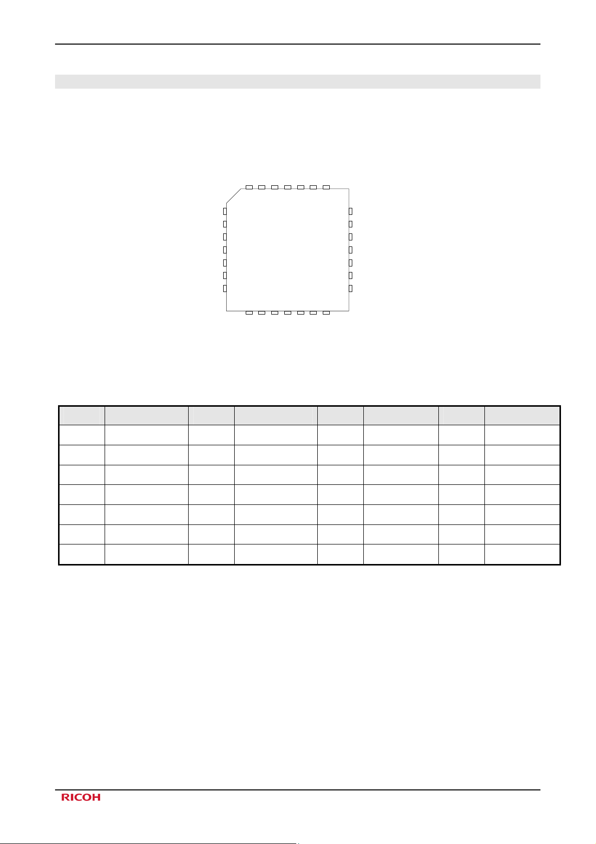
3. Pin Configuration
(TOP VIEW)
VFB2
SCL
SDA
VDD
VO5
1
2
3
4
5
6
7
GNDD
PSHOLD
Pin No. Name Pin No. Name Pin No. Name Pin No. Name
VINP2
LX2
27
28
RN5T564
9
8
VO4
VINL2
GNDP2
VINA
26
25
10
11
VREF
GNDA
VINP1
24
12
VO3
LX1
23
13
VO2
GNDP1
22
21
20
19
18
17
16
15
14
VINL1
QFN0404-28 pin
VFB1
PWRON
DC1EXON
RESETO
RESETI
VIND
VO1
1 GNDD 8 VINL2 15 VO1 22 GNDP1
2 VFB2 9 VO4 16 VIND 23 LX1
3 PSHOLD 10 VREF 17 RESETI 24 VINP1
4 SCL 11 GNDA 18 RESETO 25 VINA
5 SDA 12 VO3 19 DC1EXON 26 GNDP2
6 VDD 13 VO2 20 PWRON 27 LX2
7 VO5 14 VINL1 21 VFB1 28 VINP2
Fig 3-1 Pin Configuration
©2009 Rev. 1.4 Page 4
RN5T564 7-CHANNEL POWER MANAGEMENT IC
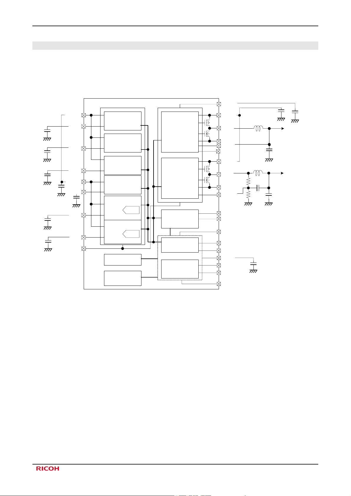
4. Block diagram
VINA
GND
GND
GND
GND
GND
1.0uF
1.0uF
1.0uF
1.0uF
2.2uF
2.2uF
GND
VINL1
VO1
VO2
VO3
VINL2
VREF
GND
VO4
VO5
GNDA
1.0uF
LDO1 150mA
Normal
LDO2 150mA
Normal
LDO3 150mA
Normal
VREF
LDO4 300mA
DAC
Normal /ECO
LDO5 300mA
DAC
Normal /ECO
UVLO
Thermal
Shutdown
Step-down
DC/DC
Converter 1
Step-down
DC/DC
Converter 2
RESET_DET
I2CI/F
Power ON
Sequence
VINP1
LX1
GNDP1
VFB1
DC1EXON
VINP2
LX2
GNDP2
VFB2
RESETO
RESETI
VIND
SDA
SCL
VDD
PWRON
PSHOLD
GNDD
4.7uH
GND
2.2uH
R1
C
R2
GND GND
(Opendrain)
0.1uF
GND
GND
10uF
4.7uF
2.2uF
1.0uF
GND
Fig 4-1 Block Diagram
©2009 Rev. 1.4 Page 5
RN5T564 7-CHANNEL POWER MANAGEMENT IC
5. Pin Description
No. Name I/O
1 GNDD G Ground GND
2 VFB2 I Output voltage feedback input of DCDC converter -
3 PSHOLD I Input signal to maintain power on VDD
4 SCL I I2C interface clock input VDD
5 SDA I/O I2C interface data input VDD
6 VDD PWR Power supply for Interface VDD
7 VO5 O LDO5 output -
8 VINL2 PWR Power supply VIN
9 VO4 O LDO4 output -
10 VREF O Bypass capacitor connecting pin -
11 GNDA G Ground GND
12 VO3 O LDO3 output -
13 VO2 O LDO2 output -
14 VINL1 PWR Power supply VIN
15 VO1 O LDO1 output -
16 VIND PWR Power supply VIN
17 RESETI I RESET in VIN
18 RESETO O RESET out VIN Open Drain
19 DC1EXON I DCDC1 ON/OFF input VIN
20 PWRON I Power ON signal input VIN
21 VFB1 I Output voltage feedback input of DCDC converter -
22 GNDP1 G Ground GND
23 LX1 O DCDC converter switch output -
24 VINP1 PWR Power supply for LDOs VIN
25 VINA PWR Power supply VIN
26 GNDP2 G Ground GND
27 LX2 O DCDC converter switch output -
28 VINP2 PWR Power supply VIN
Function I/F Level Notes
Connect only
Capacitor load
Table 5-1 Pin Description
©2009 Rev. 1.4 Page 6
RN5T564 7-CHANNEL POWER MANAGEMENT IC
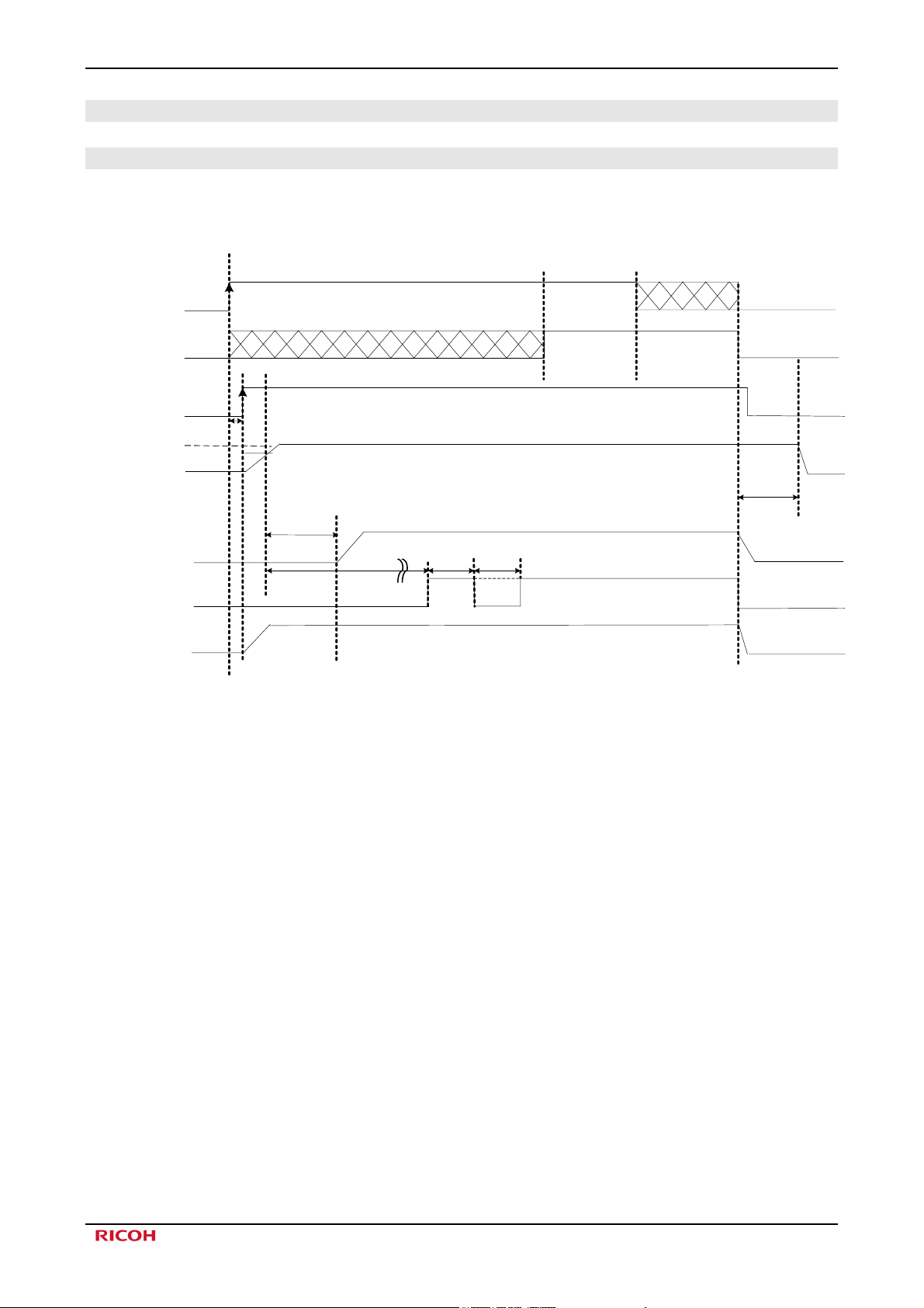
6. Power ON/OFF Operation
6.1 Power ON/OFF Operation
Power on/off Operation: Both “1ms” and “10ms” period of the following timing are min standards.
PWRON
Pull PS_HOLD "H" to keep power on before power-on factor goes low.
PSHOLD
Sync
PWRON
100us(max)
VCC33
(DCDC2 output )
90%
100us
10ms
Vcore
(DCDC1 output )
RESETO
LDO1,2,3
Note*1: Generating “L” pulse can be selected by trimming.
100ms
1ms 1ms
*1
Fig 6-1 Power ON/OFF Timing
(a) Power ON by external signal: PWRON pin
When PWRON pin becomes “H” in synchronization with the internal clock, the power-on sequence starts.
DCDC1, DCDC2, LDO1, LDO 2 and LDO 3 power on following the power-on sequence in the above timing chart.
After “L”pulse output of RESETO signal for 1ms, it need to push PSHOLD signal “H”.
The power-on state can be held by PSHOLD signal= “H” during PWRON=“H”
Note*: The default of DC1ON (Refer to Table 10-1, 2) is “H".
When both DC1ON and DC1EXON are “H”, DCDC1 turns on.
The power-on sequence will be the following. (Refer to Fig. 6-1)
(b) Power OFF operation
If PSHOLD signal goes “L”, Power-off sequence will be asserted, and then DCDC1, LDO1, LDO2, LDO3, LDO4
and LDO5 turn off immediately. However, DCDC2 will turn off with 100 us of delay time.
©2009 Rev. 1.4 Page 7
RN5T564 7-CHANNEL POWER MANAGEMENT IC
6.2 UVLO (Under Voltage Lock Out) Electrical Characteristics
Operating Conditions (unless otherwise specified) Ta = 25℃
Symbol Parameter Condition Min Typ Max Units
V
V
V
Release
Detect
HYS
Under voltage lock out threshold VCCVIN rising 2.80 V
Under voltage lock out threshold VCCVIN falling 2.70 V
UVLO Hysteresis - 100 mV
Table 6-1 UVLO Electrical Characteristics
6.3 Thermal Shutdown Circuit Electrical Characteristics
Operating Conditions (unless otherwise specified) VIND = 3.6V
Symbol Parameter Condition Min Typ Max Units
T
DET
Detected
Temperature
- 140 ℃
T
RET
Return Temperature - 110 ℃
Table 6-2 Thermal Shutdown Circuit Electrical Characteristics
©2009 Rev. 1.4 Page 8

RN5T564 7-CHANNEL POWER MANAGEMENT IC
7. Reset Function
After DCDC2 output is rising, RESETO signal will be “H” after 100ms from the detection voltage detected.
(Refer to 6.1.1 Power ON/OFF Operation)
RESETI
Hysteresis
Comparator
*1
RESETO
100ms
Note*1: Generating “L” pulse can be selected by trimming .
Fig 7-1 RESETO Timing
When it is generated either of the following 3 states, the power-on sequence and the register will be forced to be reset
and 5T564 can not power on as long as this state is released.
In addition, if it is generated either one of the above-mentioned 3 states during the power-on, 5T564 will power off
immediately.
・ When VIND pin voltage is below UVLO detection voltage.
・ When the thermal shutdown detects overheating.
・ When the over current detection state of DCDC1 and 2 continues over the protection delay time (1.5ms).
The power-on sequence circuit and the register are forced to be reset if:
・ VDD voltage decreases and RESETI pin is under 2.70V.
In order to power on 5T564 again, it needs to input “H” to PWRON pin.
If the above case is generated during the power-on, 5T564 will power off immdeately.
Once PWRON sequence or PWROFF sequence has started, the sequence operation will not be affected by PWRON and
PSHOLD signals.
©2009 Rev. 1.4 Page 9

RN5T564 7-CHANNEL POWER MANAGEMENT IC
8. FUNCTION Blocks
8.1 LDO, DCDC Table
LDO1 LDO2 LDO3 LDO4 LDO5 DCDC1 DCDC2
Current Capability 150mA 150mA 150mA 300mA 300mA 500mA
Initial Value 1.2V 1.3V 3.3V 3.0V 3.0V 1.30V 3.3V
Mode Normal Normal Normal Normal / ECO Normal / ECO PWM / VFM One Shot PWM
Output Voltage
Range
(PLL) (AVDD I/O) (CPU Core) (-) (-) (CPU Core) (CPU I/O)
1.2~3.3V by trimming
1.2/1.3/1.4/1.8/
2.5/2.7/3.0//3.3
by register
1.2/1.3/1.4/1.8/
2.5/2.7/3.0//3.3
by register
0.9~1.6V
by trimming
500mA
(*1)
0.9~3.3V
by external
resistor
Initial State
ON/OFF Control
Bypass Capacitance
)
(C
OUT
I2C I2C I2C I2C I2C I2C /Pin I2C
1.0uF 1.0uF 1.0uF 2.2uF
Note*1: Refer to page3
ON ON ON OFF OFF ON ON
2.2uF
10uF
4.7uH
4.7uF
2.2uH
Table 8-1 LDO, DCDC Table
©2009 Rev. 1.4 Page 10

RN5T564 7-CHANNEL POWER MANAGEMENT IC
8.2 LDO
Outline
LDO1, 2, 3 in Normal mode, LDO4, 5 in Normal and ECO mode and VREF circuit are integrated.
LDO1, 2, 3 are default ON and turned on power on sequence.
LDO integrates the limit circuit and controls the current under Ioutmax at short-circuited
ECO mode is only for light load such as standby and it operates at low current.
The switching between Normal mode and ECO mode is performed after the period of the overlap (150 us).
During the overlap period, LDO will operate with the characteristics of ECO mode. And also it is prohibited to change
the mode during this term.
VREF circuit is only for the internal reference voltage, so it can not be used as the external reference voltage.
The timing operation mode switching is shown below.
Mode
Normal Mode ECO Mode Normal Mode
Normal_ON
ECO_ON
Normal
Output
ECO Output
Overlap Overlap
Table 8-2 LDO4, 5 Mode Change Timing
©2009 Rev. 1.4 Page 11

RN5T564 7-CHANNEL POWER MANAGEMENT IC
8.2.1 LDO1, 2, 3 Electrical Characteristics
Operating Conditions (unless otherwise specified) VINL
= 3.6V, C
= 1.0μF, Ta = 25℃
REFO
Symbol Parameter Condition Min Typ Max Units
VOUT1,2,3 Output Voltage
Iload=50uA & VINL=4.5V
Iload=150mA & VINL=3.1V
VOUT1,2,3+0.3V≦VINL≦4.5V
-3%
1.2~
3.30*
+3% V
1
IOUT1,2,3 Output Current - 150 mA
ILIM1,2,3 Current Limit VOUT1,2,3=1.2V 400 mA
VDRP1,2,3 Drop-out Voltage
ΔVOUT1,2,3
ΔVIN
ΔVOUT1,2,3
Line Regulation
Load Regulation
IOUT1,2,3=150mA, T
VOUT1,2,3+0.3V≦V
IOUT1,2,3=75mA
50μA<IOUT1,2,3<150mA
=85℃
a
(VIN)≦4.5V
BATT
300 mV
3 mV
25 mV
ΔIOUT1,2,3
ΔVOUT1,2,3
ΔT
a
RR1,2,3 Ripple Rejection
ISS1,2,3 Supply Current
Output Voltage
Temperature
Coefficient
-40℃≦T
f=10Hz-10kHz, C
≦85℃
a
out
=1.0μF
IOUT1,2,3=30mA,VOUT≦3.0V
Normal
+100
ppm/
℃
60 dB
70
μA
OFF 1
Table 8-3 LDO1, 2, 3 Electrical Characteristics
Note*1: The output voltage will be fixed (with 0.05V step) by trimming at shipment.
Note*: Bypass capacitor: 1.0uF, in mounted state.
For optimized phase compensation, the bypass capacitor must be ceramic type.
©2009 Rev. 1.4 Page 12

RN5T564 7-CHANNEL POWER MANAGEMENT IC
8.2.2 LDO4, 5 Electrical Characteristics
Operating Conditions (unless otherwise specified) VINL
= 3.6V, C
= 2.2μF, Ta = 25℃
REFO
Symbol Parameter Condition Min Typ Max Units
VOUT4,5 Output Voltage
Iload=50uA & VINL=4.5V
Iload=150mA & VINL=3.1V
VOUT4,5+0.3V≦VINL≦4.5V
-3%
1.2~
3.30
+3% V
IOUT4,5 Output Current - 300 mA
ILIM4,5 Current Limit VOUT4,5=3.3V 500 mA
VDRP4,5 Drop-out Voltage IOUT4,5=300mA, Ta =85℃ 300 mV
ΔVOUT4,5
ΔVIN
ΔVOUT4,5
ΔIOUT4,5
ΔVOUT4,5
ΔT
a
Line Regulation
Load Regulation 50μA<IOUT4,5<300mA 35 mV
Output Voltage
Temperature
Coefficient
RR4,5 Ripple Rejection
ISS4,5 Supply Current
VOUT4,5+0.3V≦V
(VIN)≦4.5V
BATT
IOUT4,5=150mA
-40℃≦T
f=10Hz-10kHz, C
≦85℃ +100 ppm/℃
a
=2.2μF
out
IOUT4,5=30mA, VOUT≦3.0V
Normal 50
OFF 1
3 mV
60 dB
μA
1.2
1.3
1.4
POUT4,5
Programmable
Output Voltage
IOUT4, 5=300mA -3%
1.8
+3% V
2.5
2.7
3.0
3.3
Table 8-4 LDO4, 5 Normal Mode Electrical Characteristics
Note*: Bypass capacitor: 2.2uF, in mounted state.
For optimized phase compensation, the bypass capacitor must be ceramic type.
2) ECO mode
Operating Conditions (unless otherwise specified) VINL
= 3.6V, Ta = 25℃
Symbol Parameter Condition Min Typ Max Units
VOUT4,5 Output Voltage IOUT4,5= 5mA -3% 3.3 +3% V
IOUT4,5 Output Current - 5 mA
Iss Supply Current IOUT= 0mA 5 uA
Table 8-5 LDO4, 5 ECO Mode Electrical Characteristics
©2009 Rev. 1.4 Page 13

RN5T564 7-CHANNEL POWER MANAGEMENT IC
8.3 Step-down DC/DC Converter
8.3.1 Step-down DC/DC Converter1 Electrical Characteristics
PWM Mode Vin=3.6V, Cout=10μF, L=4 .7μH
Symbol Parameter Condition Min Typ Max Units
Vin Input Voltage - 3.1 4.5 V
Vout Output Voltage Range - 0.9 1.3 1.6 V
Vacc Output Voltage Accuracy 10μA≦Iout≦600mA
Vo u t
-35
Vstep Setup Voltage Step - 5 mV
ΔV/ΔT
Output Voltage
Temperature Coefficient
-40℃≦Ta≦85℃ ±40 ±150
Fosc Switching Frequency - 1.2 1.5 1.8 MHz
Iout Maximum Output Current - 600 mA
Ilimit Limit Current Peak Current 800 1000 1200 mA
Vpeak Load Transient Response
Iout=1mA⇔600mA、Δt=3μs
Vo u t = 1 . 3 V
±50 mV
VripO Ripple Voltage Iout=300mA ±5 mV
Vo u t
+35
mV
ppm
/℃
Eff Efficiency Vout=1.3V, Iout=100mA 80 %
Tprot Protect Delay Time Vin=3.6V 1.5 msec
Tri Rising Time Vout=1.3V(0→90%), Iout=0mA 0.2 msec
Tfa Falling Time Vout=1.3V(1.3→0.3V), Iout=0mA 0.5 msec
Iss Supply Current
Open Loop(VFB=Vin)
Iout=0mA
200 uA
Isd Standby Current OFF state 0.1 uA
Table 8-6 Step-down DC/DC Converter1 PWM Mode Electrical Characteristics
VFM Mode Vin=3.1V~4.5V, Cout=10μF, L = 4.7μH
Symbol Parameter Condition Min Typ Max Units
Vin Input Voltage - 3.1 4.5 V
Vout Output Voltage Range - 0.9 1.3 1.6 V
Vacc Output Voltage Accuracy 10μA≦Iout≦50mA Vout-35 Vout+35 mV
Vstep Setup Voltage Step - 5 mV
ΔV/ΔT
Output Voltage
Temperature Coefficient
-40℃≦Ta≦85℃ ±40 ±150
ppm
/℃
Iout Maximum Output Current - 50 mA
VripO Ripple Voltage Iout=25mA -50 +50 mV
Eff Efficiency Vout=1.3V, Iout=1mA 60 %
Ilimit Limit Current Vin=3.6V 300 mA
Tfa Falling Time
Iss Supply Current
Vo u t = 1 . 3 V (1.3→0.3V),
Iout=0mA
Open Loop(VFB=Vin)
Iout=0mA
0.5 msec
20 μA
Table 8-7 Step-down DC/DC Converter1 VFM Mode Electrical Characteristics
©2009 Rev. 1.4 Page 14

RN5T564 7-CHANNEL POWER MANAGEMENT IC
8.3.2 Step-down DC/DC Converter2 Electrical Characteristics
Operating Conditions (unless otherwise specified) VINA, VINP = 3.6V, T
= 25℃ L1=2.2uH, C
a
OUT
=4.7uF
Symbol Parameter Condition Min Typ Max Units
- Input Voltage Range VINA, VINP pin 3.1 4.5 V
DVOUT1
Output Voltage
Range
- 0.9 3.3 V
DIOUT1 Output current VINA=VINP=3.1~4.5V 500 mA
DISS1
Consumption
Current
DIOFF1 Standby Current
DILIM1
Limit detection
Current
VINA=VINP=VFB=3.6V
DIOUT1=0mA, no switching
VINA=VINP=4.5V
OFF state
- 800 mA
70 uA
1 uA
VFB1 FB Voltage DIOUT1=1mA~500mA -1.5% 0.608 +1.5% V
ΔVFB1
ΔVIN
ΔVFB1
ΔT
*1
t
r
T
Onmin
FB Line Regulation
FB Voltage
Temperature
Coefficient
Soft-start Time - 120 us
Minimum-On-Time - 120 ns
VINA=VINP=3.1~4.5V
DIOUT=DIOUTmax / 2
TBD mV
-40℃≦Ta≦+85℃ ±100 ppm/℃
Table 8-8 Step-down DC/DC Converter2 Electrical Characteristics
Note*: Load Regulation, which is determined by DC resistance (DCR) on inductor, is given by:
Load Regulation (Typ) = DCR (Ω) ×DIOUT (A).
Note*1: When all regulators are off, Soft-start time will be added up with UVLO output delay time for release.
t
(Typ)= 120 us + 10us(UVLO output delay time for release).
r
©2009 Rev. 1.4 Page 15

RN5T564 7-CHANNEL POWER MANAGEMENT IC
8.3.3 Step-down DC/DC Converter2 Output Voltage Setting
VINA
VINP2
DCDC Enable Signal
Current
Limit
R1=R2*(DVOUT/V
-1)
FB
DVOUT=Set output voltage
V
= 0.6V (Internal reference voltage)
FB
L
R1
x 10
=
C
f
GND
L2=2.2uH
R1
R2
C
f
DVOUT
Cout= 4.7uF
GND
- DVOUT=1.2V.
R1=220kΩ, R2=220kΩ, C
- DVOUT=1.8V.
R1=220kΩ, R2=110kΩ, C
- DVOUT=3.3V.
R1=220kΩ, R2=48.9kΩ, C
=100pF
f
=100pF
f
=100pF
f
GNDA
GND
One-shot
Circuit
Sw itchin g
Control Circuit
+
Vref
Soft-start
LX 2
VFB2
GNDP2
GND
External components example
Table 8-9 Step-down DC/DC Converter 2 Output Voltage Setting
©2009 Rev. 1.4 Page 16

RN5T564 7-CHANNEL POWER MANAGEMENT IC
9. CPU Interface
RN5T564 uses I2C-Bus system for CPU connection through 2-wires.
9.1 I2C BUS
I2C-Bus is the interface which is communicated by 2-wire of SCL (Serial Clock) and SDA (Serial Data).
Connection and transfer system of I2C-Bus are described in the following sections.
9.1.1 Method of I2C-Bus Transfer
(1) Availability of Data
When data transmission, SDA should be kept in the certain state during SCL=“H”. Only when SCL is “L”, SDA state
can be changed its state except the start condition and the stop condition.
SCL
SDA
Fig 9-1 I2C-Bus Data Transmission
(2) Start condition and Stop condition
When the data transmision is not performed, both SCL and SDA are “H”. At that time, if SDA state is changed “H” to
“L”, it will be the start condition then start transmitting data. And also if SDA state is changed “L” to “H” during
SCL=“H”, it will be the stop condition then the master can stop the transmitting data. Only the master can generate the
start and stop conditions.
SCL
SDA
Start Condition
Fig 9-2 Start Condition and Stop Condition
©2009 Rev. 1.4 Page 17
Stop Condition

RN5T564 7-CHANNEL POWER MANAGEMENT IC
(3) Data Transmitting
After the start condition, the data is transmitted by 1 byte (8bits). The receiver must send an acknowledge signal to the
transmitter whenever 8bit data is transmitted.
When the master is the transmitter, it will release SDA after sending a byte and then the slave will pull SDA down to
“L” as an acknowledge signal. And, when the slave is the transmitter, it will release SDA (“H”) after sending a byte then
the master will pull SDA down to “L” as an acknowledge if it will keep receiving data.
If the master wants to stop receiving data from the slave, it will inform the end of the data transmission by not
generating acknowledge.
SCL from Master
SDA from Transmitter
SDA from Receiver
Start Condition
198765423
Acknowledge
Stop Condition
Fig 9-3 I2C-Bus Data Transmission and Acknowledge
9.1.2 I2C-Bus Slave Address
The slave address of I2C-Bus INTERFACE will be MSB first 7 bit of the first byte after the start condition (S) or the
retransmission (Sr).
The construction of address is shown below:
A7 A6 A5 A4 A3 A2 A1
A7~A1 Slave Address
The slave address of A7~A1 are specified at 0110010b.
©2009 Rev. 1.4 Page 18

RN5T564 7-CHANNEL POWER MANAGEMENT IC
9.1.3 I2C-Bus Data Transmission Format
When the data is transmitted through I2C-Bus, the transmission format is shown for each mode.
The transmitting data is performed by the 2 formats shown below. It should start at the start condition and stop at the
stop condition.
Note*: There is no high rate (Serial) R/W mixed format.
When the master transmits data, it needs to transmit a byte of the data from MSB first and the following data in
sequence.
When it receives the data from the slave, the slave needs to transmit the data from MSB first as well.
Note*: User register address should be specified within the range of 00h~02h.
It is prohibited to setting the invalid address 03h~FFh.
(1) Normal Writing Format
R/W=0(Writing)
SXXXXXXX0AXXXXXXXXAXXXXXXXXAP
Transfer of slave
address(7bit)
Selection of user
address(8bit)
Data writing in user
register(8bit)
Master is Transmitter. Master is Receiver
S Start Condition P Stop Condition
A /A A Acknowledge Signal Sr Retransmission Start Condition
Fig 9-4 I2C-Bus Data Transmission Format
©2009 Rev. 1.4 Page 19

RN5T564 7-CHANNEL POWER MANAGEMENT IC
(2) Normal Reading Format
R/W=0(Writing)
SXXXXXXX0AXXXXXXXXASr
Retransmission
start condition
Transfer of slave
address (7bit)
Selection of user
address (8bit)
R/W=1(Reading)
XXXXXXX1AXXXXXXXX/AP
Transfer of slave
Data reading (8bit)
address (7bit)
Master is Transmitter Master is Receiver
S Start Condition P Stop Condition
A /A A Acknowledge Signal Sr Retransmission Start Condition
Fig 9-5 I2C-Bus Data Read Format
©2009 Rev. 1.4 Page 20

RN5T564 7-CHANNEL POWER MANAGEMENT IC
9.1.4 I2C-Bus SDA and SCL Bus Line characteristics
AC Characteristics VDD=1.8~4.5V,Ta=-40~85℃
Parameter Symbol Condition Min Max Unit
SCL clock frequency fSCL - 0 400 kHz
Bus free time between stop condition and
start condition
Hold time (retransmission) start condition tHD;STA - 0.6 μs
Low state hold time of SCL clock tLOW - 1.3 μs
High state hold time of SCL clock tHIGH - 0.6 μs
Set up time of retransmission start
condition
Set up time of stop condition tSU;STO - 0.6 μs
Data hold time tHD;DAT - 0 μs
Data set up time tSU;DAT - 100 *1 ns
Rising time of SDA and SCL signal tR - 300 ns
Falling time of SDA and SCL signal tF - 300 ns
Rejection spike pulse range by input filter tSP - 50 ns
Capacitive load for each bus line Cb*2 - 400 pF
tBUF - 1.3 μs
tSU;STA - 0.6 μs
Table 9-1 I2C-Bus AC Characteristics
All of the above-mentioned values are corresponding to VIHmin and VILmaxlevel.
Note*1: This is the high rate mode I2C-Bus spec. The standard mode is allowed in I2C-Bus system, but it need to
satisfy the condition;
tSU;DAT≧250ns.
Note*2: Cb= Total capacitance of 1 bus line(Unit pF)
I2C-Bus Timing Chart
SDA
tBUF
tLOW
tR
tF
tHD;STA
SCL
tSP
tHD;STA tSU;DAT
tHD;DAT
tSU;STA
tSU;STO tHIGH
P S P
Sr
Fig 9-6 I2C-Bus Timing Chart
©2009 Rev. 1.4 Page 21

RN5T564 7-CHANNEL POWER MANAGEMENT IC
r
Internal Register Timing
Writing
SCL from Master
SDA from Master
SDA from Master
Internal Register
Writing Signal (WRB)
Start Condition
Reading
SCL from Master
SDA from Slave
SDA from Master
198765423
Writing data to user register
9
1
Reading data to user register
Acknowledge
Writing timing to
an internal register
9
8765423
Acknowledge
Stop Condition
Internal
Register
Latch Timing
Start Condition
When reading internal register
Latch timing
When reading next internal registe
Latching timing
Stop Condition
Fig 9-7 Internal Register Timing
(Codicil)
The 2 wires of SCL and SDA, which connected to I2C-Bus, are used for transmitting clock pulse and data individually.
All Ics connected to these two lines are designed not to be clamped even though the voltage, which exceeds its power
supply voltage, is supplied through the input and output. (The output is open-drain-circuited).
This construction allows the communication of signals between Ics, which have different supply voltages, by adding a
pull-up resistor to each signal line.
©2009 Rev. 1.4 Page 22
RN5T564 7-CHANNEL POWER MANAGEMENT IC
10. Register
The register, which is readable/ writable through I2C, controls and monitors the state of DCDC and LDO.
The register will be reset in the conditions below:
・ DCDC1, 2 over current detection
・ Overheating detection of thermal shutdown (TSHUT)
・ VIND voltage decrease detection of UVLO
・ VDD voltage decrease detection of RESET_DET
When PWRON pin is “L”, the writing register is prohibited.
The writing in the address 03h~FFh is prohibited.
10.1 Register Map
add Name R/W D7 D6 D5 D4 D3 D2 D1 D0
00h PWRON R/W DC2ON DC1ON - LDO5ON LDO4ON LDO3ON LDO2ON LDO1ON
01h MODE R/W - DC1MD - LDO5MD LDO4MD - - -
02h L45VSEL R/W - LDO5D2 LDO5D1 LDO5D0 - LDO4D2 LDO4D1 LDO4D0
Table 10-1 Register Map
©2009 Rev. 1.4 Page 23
RN5T564 7-CHANNEL POWER MANAGEMENT IC
10.2 Register Description
10.2.1 PWRON Register (Address: 00h)
The register controls ON/OFF of LDO 1-5 and DCDC1, 2.
Bit Name R/W Function 1 0
7 DC2ON
6 DC1ON
5
4 LDO5ON
3 LDO4ON
2 LDO3ON
1 LDO2ON
0 LDO1ON
- -
R/W
R/W
R/W
R/W
R/W
R/W
R/W
DCDC2 ON/OFF control bit ON OFF 1
DCDC1 ON/OFF control bit ON OFF 1
Reserved
- -
LDO5 ON/OFF control bit ON OFF 0
LDO4 ON/OFF control bit ON OFF 0
LDO3 ON/OFF control bit ON OFF 1
LDO2 ON/OFF control bit ON OFF 1
LDO1 ON/OFF control bit ON OFF 1
Table 10-2 PWRON Register
Initial
value
0
10.2.2 MODE Register (Address: 01h)
The register sets the operation mode of LDO and DCDC.
Bit Name R/W Function 1 0
7
6 DC1MD
5
4 LDO5MD
3 LDO4MD
0-2
- - - - -
R/W
DCDC1 Mode control bit
VFM PWM
- - - - -
R/W
R/W
LDO5 Mode control bit
LDO4 Mode control bit
ECO Normal
ECO Normal
- - - - -
Table 10-3 MODE Register
Initial value
0
0
0
0
0
000
©2009 Rev. 1.4 Page 24

RN5T564 7-CHANNEL POWER MANAGEMENT IC
10.2.3 LDO Setting Voltage Register (Address: 02h)
The register sets the output voltage of LDO4 and 5.
Bit Name R/W Function 1 0
7
6-4
3
2-0
- -
LDO5D[2:0] R/W
- -
LDO4D[2:0] R/W
Reserved
As below
Reserved
As below
As below
As below
Table 10-4 LDO Setting Voltage Register
LDO4D [2:0] LDO5D [2:0]
Initial
value
-
0
110
-
0
110
LDO4D[2] LDO4D[1]
1 1 1 3.3V 1 1 1 3.3V
1 1 0 3.0V 1 1 0 3.0V
1 0 1 2.7V 1 0 1 2.7V
1 0 0 2.5V 1 0 0 2.5V
0 1 1 1.8V 0 1 1 1.8V
0 1 0 1.4V 0 1 0 1.4V
0 0 1 1.3V 0 0 1 1.3V
0 0 0 1.2V 0 0 0 1.2V
LDO4D[0] LDO4 Voltage
LDO5D[2] LDO5D[1]
LDO5D[0] LDO5 Voltage
©2009 Rev. 1.4 Page 25

RN5T564 7-CHANNEL POWER MANAGEMENT IC
11. Electrical Characteristics
11.1 Absolute Maximum Ratings
The operation exceeding “Absolute Maximum Ratings”below may cause not only permanent damage to the device, but
also reliability and safeness of its equipment. The operation of the device within the stated ratings below is not
guaranteed.
Symbol Parameter Condition Rated Value Units
V
IN
V
PIN
PD
T
stg
11.2 Recommendation of Operation Conditions
Symbol Parameter Condition Min Typ Max Units
VIN Power Supply Voltage1 Battery Voltage Input Pins 3.1 3.6 4.5 V
VDD Power Supply Voltage
T
a
Power Input Voltage VINP*, VIN*, VDD -0.3~6.0 V
Signal Input
Voltage Range
Package
Allowable Dissipation
SCL, SDA, PSHOLD -0.3~VDD+0.3 V
PWRON, DC1EXON -0.3~VIND+0.3 V
Mounted on Board,
=70℃
T
a
1500 mW
Storage Temperature - -55~+125 ℃
Temperature of Operation
-
-
1.8 3.3 4.5 V
-40 +85 ℃
11.3 System Consumption Current
Operating Conditions (unless otherwise specified) VIND = 3.6V
Symbol Parameter Condition Min Typ Max Units
Iccd
Iccs
Consumption current
at power on
Consumption current
at power off
PWRON=H, VIND Input Current
(UVLO, RESET_DET, TSHUT,OSC)
PWRON=L, VIND Input Current
(Standby Current)
30 uA
1 uA
©2009 Rev. 1.4 Page 26

RN5T564 7-CHANNEL POWER MANAGEMENT IC
12. Electrical Characteristics of Digital Input/Output Pin
12.1 VDD system CMOS Schmitt Input Pin
Operating Conditions (unless otherwise specified) VIND = 3.6V, Ta = 25℃
Applicable pin: SCL, SDA
Parameter Symbol Condition Min Typ Max Unit
Input leakage ILI
Input rising threshold voltage VT+
Input falling threshold
voltage
Hysteresis range ΔVT
VT-
Vin =0~VDD
-
-
-
12.2 VDD system Nch Open Drain Output Pin
Applicable pin: SDA
Parameter Symbol Condition Min Typ Max Unit
Output voltage L level VOL Iout=-3mA 0.4 V
-1 1 μA
VDD×0.5 VDD×0.7 V
VDD×0.3 VDD×0.5 V
VDD×0.1 V
12.3 VIND system CMOS Schmitt Input Pin
Applicable pin: PWRON
Parameter Symbol Condition Min Typ Max Unit
Input leakage ILI
Input rising threshold voltage VT+ - VIND×0.5 VIND×0.8 V
Input falling threshold voltage VT- - VIND×0.2 VIND×0.5 V
Hysteresis range ΔVT - VIND×0.1 V
Applicable pin: DC1EXON
Parameter Symbol Condition Min Typ Max Unit
Input leakage ILI
Input rising threshold voltage VT+ -
Input falling threshold voltage VT- -
Hysteresis range ΔVT -
Vin =0~VIND
Vin =0~VIND
-1 1 μA
-1 1 μA
0.6 1.2 1.8
0.4 0.8 1.2
0.1 0.4 0.7
V
V
V
12.4 VDD system CMOS Input pin
Applicable pin: PSHOLD
Parameter Symbol Condition Min Typ Max Unit
Input leakage ILI
Input voltage H level VIH - VDD×0.7 V
Input voltage L level VIL - VDD×0.3 V
Vin =0~VDD
-1 1 μA
12.5 VIND system NchOpen Drain Output Pin
Applicable pin: RESETO
Parameter Symbol Condition Min Typ Max Unit
Output voltage L level VOL Iout=-3mA 0.4 V
©2009 Rev. 1.4 Page 27

RN5T564 7-CHANNEL POWER MANAGEMENT IC
13. Package Information
©2009 Rev. 1.4 Page 28
 Loading...