


Power Management System Device
RN5T561-0000
Development Specifications
Rev. 1.3
2009.05.19
RICOH COMPANY, LTD.
Electronic Devices Company
This specification is subject to change without notice.

RN5T561-0000 POWER MANAGEMENT SYSTEM DEVICE
Contents
1.
Outline....................................................................................................................................................................3
2. Feature ...................................................................................................................................................................3
3. Pin Configuration..................................................................................................................................................4
4. Block Diagram.......................................................................................................................................................5
5. Pin Description ......................................................................................................................................................6
6. Power On/Off Control ..........................................................................................................................................7
6.1 UVLO (Under Voltage Lock Out) ...................................................................................................................7
7. Functional Blocks.................................................................................................................................................. 8
7.1 Regulators..........................................................................................................................................................8
7.1.1 Operation Mode Control............................................................................................................................ 9
7.1.2 LDO1 Electrical Characteristics .............................................................................................................. 10
7.1.3 LDO2 Electrical Characteristics (IO/LCD) ............................................................................................. 11
7.1.4 LDO3 Electrical Characteristics (USB)................................................................................................... 12
7.1.5 LDO4 Electrical Characteristics (Analog/Audio).................................................................................... 13
7.1.6 VREF and IREF Electrical Characteristics.............................................................................................. 13
7.2 Step-down DC/DC Converter ........................................................................................................................14
7.2.1 Step-down DC/DC Converter Block Diagram.........................................................................................14
7.2.2 Target Electrical Characteristics .............................................................................................................. 15
7.2.3 Recommended External Component ....................................................................................................... 15
7.3 Thermal Shutdown Circuit ............................................................................................................................16
7.3.1 Thermal Shutdown Electrical Characteristics.......................................................................................... 16
7.4 CPU Interface..................................................................................................................................................17
7.4.1 Start and Stop Condition.......................................................................................................................... 17
7.4.2 Data Transmission and its Acknowledge ................................................................................................. 18
7.4.3 I2C-Bus Slave Address............................................................................................................................ 18
7.4.4 Data Transmission Write Format ............................................................................................................. 19
7.4.5 Internal Register Write-in Timing............................................................................................................ 19
7.4.6 AC Characteristics of I2C-Bus ................................................................................................................ 20
8. Register ................................................................................................................................................................21
8.1 Register Map ...................................................................................................................................................21
8.2 DC/DC Converter Control Register: DCCTL (Command 000b) ...............................................................21
©2009 Rev. 1.3 Page 1

RN5T561-0000 POWER MANAGEMENT SYSTEM DEVICE
8.3 LDO Control Register: LDOCTL (Command 001b)...................................................................................21
8.4 Mode Control Register: MODECTL (Command 010b)..............................................................................21
9. Electrical Characteristics ...................................................................................................................................22
9.1 Absolute Maximum Ratings...........................................................................................................................22
9.2 Recommended Operation Conditions ...........................................................................................................22
9.3 DC Characteristics..........................................................................................................................................23
10. Package Information...........................................................................................................................................24
©2009 Rev. 1.3 Page 2

RN5T561-0000 POWER MANAGEMENT SYSTEM DEVICE
1. Outline
RN5T561 is the power management IC, which contains the power supply, the power supply control function and etc. in
one-chip.
2. Feature
z Power Supply Function
9 Power supply control function
z One Step-down DC/DC converter
9 ON/OFF programmable through I2C
9 PWM control
9 DCDC output voltage settable by external resistor
z Four LDO Regulators
9 ON/OFF programmable through I2C (Except LDO2)
9 ECO-mode for LDO1, 2 and 3: Programmable through I2C
9 LDO1 output voltage: Selectable by trimming work
z I2C-Bus (Max 400kHz)
9 Slave address = 32h
9 LDO, DC/DC converter control
z UVLO
9 Monitoring VIN2 voltage
z Package
9 16pin QFN package (Body size: 3 x 3 x 0.85mm, Pin pitch: 0.4mm)
z Process
9 CMOS process
©2009 Rev. 1.3 Page 3
RN5T561-0000 POWER MANAGEMENT SYSTEM DEVICE
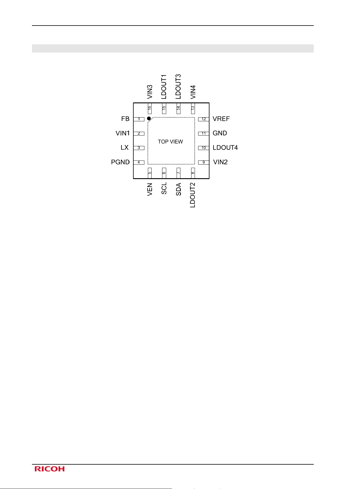
3. Pin Configuration
Fig 3-1 Pin Configuration
©2009 Rev. 1.3 Page 4
RN5T561-0000 POWER MANAGEMENT SYSTEM DEVICE
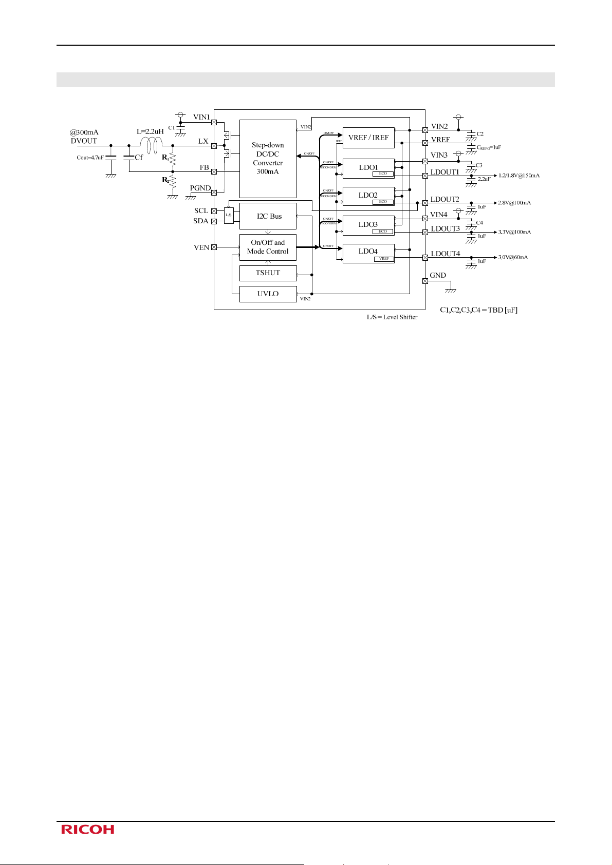
4. Block Diagram
Fig 4-1 Block Diagram
©2009 Rev. 1.3 Page 5
RN5T561-0000 POWER MANAGEMENT SYSTEM DEVICE
5. Pin Description
NO NAME I/O FUNCTION NOTES
1 FB I Output voltage feedback of DC/DC converter
2 VIN1 PWR Power supply for DC/DC converter
3 LX O Switch output of DC/DC converter circuit
4 PGND GND Power GND for DC/DC converter
5 VEN I Power-on signal Schmitt /pull-down
6 SCL I Clock input for I2C-Bus Schmitt
7 SDA I/O Data input/output for I2C-Bus Schmitt /Nch Open-drain
8 LDOUT2 O Output of LDO2
9 VIN2 PWR Power supply for VREF, LDO2 and 4
10 LDOUT4 O Output of LDO4
11 GND GND GND
12 VREF O Capacitor connection for reference Do not load this pin.
13 VIN4 PWR Power supply for LDO3
14 LDOUT3 O Output of LDO3
15 LDOUT1 O Output of LDO1
16 VIN3 PWR Power supply for LDO1
Table 5-1 Pin Description
©2009 Rev. 1.3 Page 6

RN5T561-0000 POWER MANAGEMENT SYSTEM DEVICE
6. Power On/Off Control
Fig 6-1 Power On/Off Timing
RN5T561 can be asserted power on by pushing VEN pin high but UVLO signal should be high by detecting the battery
voltage over 3.1V. Step-down DC/DC converter turns on 250us after VEN pin goes high and then LDO1and 2 turn on.
Then LDO3 and 4 are turned on with 120us of time interval.
When VEN goes low, all LDOs, DC/DC converter and logics are powered off and all register will be reset.
Note*: Wait more than 1ms to repower on by VEN= “H”.
6.1 UVLO (Under Voltage Lock Out)
Operating Conditions (unless otherwise specified) Ta = 25℃
Symbol Parameter Condition Min Typ Max Units
V
Under voltage lock out threshold VCCVIN rising 2.25 V
Release
V
Under voltage lock out threshold VCCVIN falling 2.05 2.20 2.35 V
Detect
V
UVLO Hysteresis - 50 mV
HYS
Table 6-1 UVLO
©2009 Rev. 1.3 Page 7
 Loading...