


LO W DROP-OUT AND LO W NOISE
V OLTA GE REGULAT OR
RN5RZ SERIES
NO.EA-039-9803
APPLICATION MANUAL
ELECTRONIC DEVICES DIVISION

NOTICE
1. The products and the product specifications described in this application manual are subject to change or discontinuation of production without notice for reasons such as improvement. Therefore, before deciding to use
the products, please refer to Ricoh sales representatives for the latest information thereon.
2. This application manual may not be copied or otherwise reproduced in whole or in part without prior written consent of Ricoh.
3. Please be sure to take any necessary formalities under relevant laws or regulations before exporting or otherwise taking out of your country the products or the technical information described herein.
4. The technical information described in this application manual shows typical characteristics of and example
application circuits for the products. The release of such information is not to be construed as a warranty of or a
grant of license under Ricoh's or any third party's intellectual property rights or any other rights.
5. The products listed in this document are intended and designed for use as general electronic components in
standard applications (office equipment, computer equipment, measuring instruments, consumer electronic
products, amusement equipment etc.). Those customers intending to use a product in an application requiring
extreme quality and reliability, for example, in a highly specific application where the failure or misoperation of
the product could result in human injury or death (aircraft, spacevehicle, nuclear reactor control system, traffic
control system, automotive and transportation equipment, combustion equipment, safety devices, life support
system etc.) should first contact us.
6. We are making our continuous effort to improve the quality and reliability of our products, but semiconductor
products are likely to fail with certain probability. In order prevent any injury to persons or damages to property
resulting from such failure, customers should be careful enough to incorporate safety measures in their design,
such as redundancy feature, fire-containment feature and fail-safe feature. We do not assume any liability or
responsibility for any loss or damage arising from misuse or inappropriate use of the products.
7. Anti-radiation design is not implemented in the products described in this application manual.
8. Please contact Ricoh sales representatives should you have any questions or comments concerning the products or the technical information.
June 1995

OUTLINE
......................................................................................................
1
FEATURES
....................................................................................................
1
APPLICATIONS
.............................................................................................
1
BLOCK DIAGRAMS
.......................................................................................
2
SELECTION GUIDE
.......................................................................................
2
PIN CONFIGURATION
...................................................................................
3
PIN DESCRIPTIONS
......................................................................................
3
ABSOLUTE MAXIMUM RATINGS
...................................................................
3
ELECTRICAL CHARACTERISTICS
................................................................
4
OPERATION
..................................................................................................
6
TEST CIRCUITS
............................................................................................
6
TYPICAL CHARACTERISTICS
.......................................................................
8
1) Output Voltage vs. Output Current
.....................................................................
8
2) Output Voltage vs. Input Voltage
.......................................................................
8
3) Dropout Voltage vs. Output Current
...................................................................
9
4) Output Voltage vs. Temperature
......................................................................
10
5) Supply Current vs. Input Voltage
.....................................................................
10
6) Supply Current vs. Temperature
......................................................................
11
7) Dropout Voltage vs. Set Output Voltage
.............................................................
12
8) Ripple Rejection vs. Frequency
......................................................................
12
9) Ripple Rejection vs. Input Voltage (DC bias)
.......................................................
14
10) Line Transient Response
..............................................................................
14
11) Load Transient Response
.............................................................................
15
FOR STABLE OPERATION
...........................................................................
17
POWER DISSIPATION
..................................................................................
19
PACKAGE DIMENSION
................................................................................
20
TAPING SPECIFICATION
..............................................................................
20
RN5RZ SERIES
APPLICATION MANUAL
CONTENTS

LOW DROP-OUT AND LOW NOISE
VOLTAGE REGULATOR
1
RN5RZ SERIES
OUTLINE
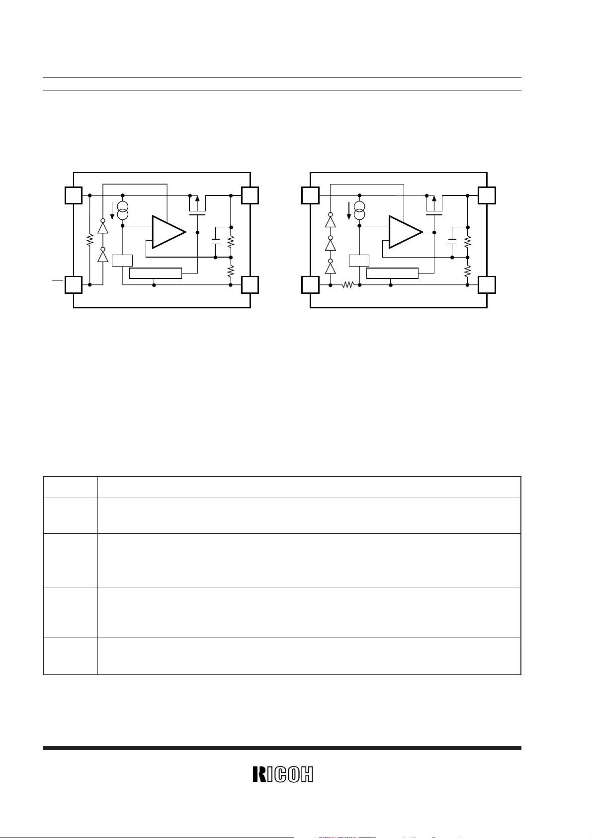
The RN5RZ Series are voltage regulator ICs with high output voltage accuracy, low supply current, low dropout
voltage and high ripple rejection developed through the use of a CMOS process. Each of these voltage regulator
ICs consists of a voltage reference unit, an error amplifier, output voltage setting resistors, a current limit circuit and
a chip enable circuit. (Provided two types of chip enable circuit ; “H” active and “L” active, that can be selected when
order.)
The output voltage of these ICs is fixed with high accuracy.
In addition to low supply current from CMOS process, the RN5RZ Series may lengthen battery life through low
dropout voltage and chip enable function thanks to the built-in low ON resistance transistor. Also when compared
with conventional regulators that employ CMOS process, these ICs have superior ripple rejection, input transient
response characteristic and load transient response characteristic thus making these product suitable for power sup-
ply for hand-held communication equipment.
Since the package for these ICs is the SOT-23-5 package, high density mounting of the ICs on boards is possible.
• Ultra-Low Supply Current
...........................................
TYP. 20µA
• Ultra-Low Supply Current (Standby)
.........................
TYP. 0.1µA
• High Accuracy Output Voltage
..................................
±2.0%
• High Ripple Rejection
.................................................
TYP.55dB (f=1kHz)
• Low Dropout Voltage
..................................................
TYP. 0.2V (I
OUT=60mA)
• Low Temperature-Drift Coefficient of Output Voltage
........
TYP. ±100ppm/˚C
• Excellent Line Regulation
...........................................
TYP. 0.05%/V
• Output Voltage
.............................................................
Stepwise setting with a step of 0.1V in the range of 2.0V to 6.0V
is possible (refer to Selection Guide).
• Built-in Short Current Limit Circuit
...........................
TYP. 50mA
• Small Package
..............................................................
SOT-23-5 (Mini-mold)
FEATURES
APPLICATIONS
• Power source for battery-powered equipment.
• Power source for cellular phones, cameras, VCRs, camcorders, hand-held audio instruments and hand-held com-
munication equipment.
• Power source for domestic appliances.
SELECTION GUIDE
RN5RZ
2
BLOCK DIAGRAMS
2
5
1
V
OUT
GND
V
DD
CE
Vref
3
Current Limit
2
5
1
V
OUT
GND
V
DD
CE
+
–
Vref
3
Current Limit
+
–
RN5RZ××A
RN5RZ
××B
RN5RZ ××××–××←Part Number
↑ ↑↑ ↑
a b c d
}
The output voltage, the active type of the chip enable circuit, the packing type, and the taping type for the ICs
can be selected at the user's request.
These selections can be made by designating the part number as shown below:
Code Contents
a
Setting Output Voltage (V
OUT) :
Stepwise setting with a step of 0.1V in the range of 2.0V to 6.0V is possible.
Designation of Active Type of The Chip Enable Circuit :
b A : “L” active type
B : “H” active type
Designation of Packing Type :
c A : Taping
C : Antistatic bag (for Samples only)
d
Designation of Taping Type :
Ex. TR, TL (refer to Taping Specifications ; TR type is the standard direction.)
}
For example, the product with Output Voltage of 5.0V, Specified Polarity of Chip Enable is “H” active and Taping
Type TR is designated by Part Number RN5RZ50BA-TR.
RN5RZ
3
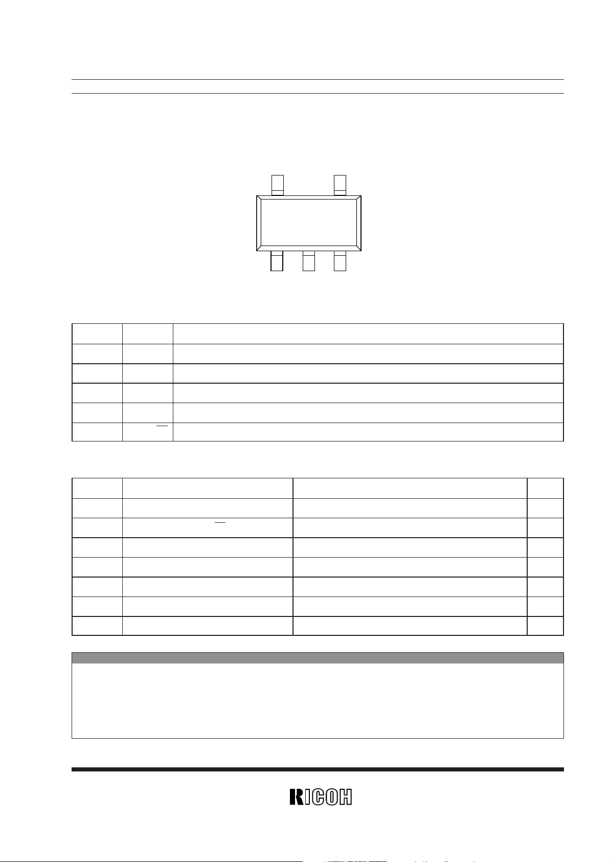
PIN CONFIGURATION
PIN DESCRIPTION
• SOT-23-5
1 2
3
5 4
(mark side)
Pin No. Symbol Description
1 GND Ground Pin
2 VDD
Input Pin
3 VOUT Output Pin
4 NC No Connection
5 CE or CE Chip Enable Pin
ABSOLUTE MAXIMUM RATINGS
ABSOLUTE MAXIMUM RATINGS
Absolute Maximum ratings are threshold limit values that must not be exceeded even for an instant under
any conditions. Moreover, such values for any two items must not be reached simultaneously. Operation
above these absolute maximum ratings may cause degradation or permanent damage to the device. These
are stress ratings only and do not necessarily imply functional operation below these limits.
Symbol Item Ratings Unit
VIN Input Voltage 9 V
VCE Input Voltage (CE or CE Pin) –0.3 to VIN +0.3 V
VOUT Output Voltage –0.3 to VIN +0.3 V
IOUT Output Current 200 mA
PD Power Dissipation 250 mW
Topt Operating Temperature –40 to +85 ˚C
Tstg Storage Temperature –55 to +125 ˚C
RN5RZ
4
ELECTRICAL CHARACTERISTICS
• RN5RZ××A Series
Symbol Item Conditions MIN. TYP. MAX. Unit
VOUT Output Voltage VIN=VOUT+1V, IOUT=30mA ×0.98 ×1.02 V
I
OUT Output Current
V
IN=VOUT+1V
100 mA
When VOUT=VOUT–0.1V
∆V
OUT
Load Regulation
V
IN=VOUT+1V
20 40 mV
∆I
OUT
1mA≤IOUT≤80mA
VDIF Dropout Voltage IOUT=60mA 0.2 0.3 V
ISS Supply Current VIN=VOUT+1V 20 40 µA
Istandby Supply Current (Standby) V
IN=VCE=VOUT+1V 0.1 1.0 µA
∆V
OUT
Line Regulation
I
OUT=30mA
0.05 0.20 %/V
∆VIN
VOUT+0.5V≤VIN≤8V
RR Ripple Rejection
f=1kHz, Ripple 0.5Vrms
55 dB
VIN=VOUT+1V
VIN Input Voltage 8 V
∆V
OUT
Output Voltage IOUT=30mA
±100
ppm/˚C
∆Topt
Temperature Coefficient –40˚C≤Topt≤85˚C
Ilim Short Current Limit VOUT=0V 50 mA
RPU CE Pull-up Resistance 2.5 5 10 MΩ
VCEH CE Input Voltage “H” 1.5 V
V
CEL CE Input Voltage “L” 0 0.25 V
Topt=25˚C

RN5RZ
5
• RN5RZ
××B Series
Symbol Item Conditions MIN. TYP. MAX. Unit
VOUT Output Voltage VIN=VOUT+1V, IOUT=30mA ×0.98 ×1.02 V
I
OUT Output Current
V
IN=VOUT+1V
100 mA
When VOUT=VOUT–0.1V
∆V
OUT
Load Regulation
V
IN=VOUT+1V
20 40 mV
∆IOUT
1mA≤IOUT≤80mA
VDIF Dropout Voltage IOUT=60mA 0.2 0.3 V
ISS Supply Current VIN=VOUT+1V 20 40 µA
Istandby Supply Current (Standby) VIN=VOUT+1V, VCE=GND 0.1 1.0 µA
∆V
OUT
Line Regulation
I
OUT=30mA
0.05 0.20 %/V
∆VIN
VOUT+0.5V≤VIN≤8V
RR Ripple Rejection
f=1kHz, Ripple 0.5Vrms
55 dB
VIN=VOUT+1V
VIN Input Voltage 8 V
∆V
OUT
Output Voltage IOUT=30mA
±100
ppm/˚C
∆Topt
Temperature Coefficient –40˚C≤Topt≤85˚C
Ilim Short Current Limit VOUT=0V 50 mA
RPU CE Pull-down Resistance 2.5 5 10 MΩ
VCEH CE Input Voltage “H” 1.5 V
V
CEL CE Input Voltage “L” 0 0.25 V
Topt=25˚C
 Loading...