

VFM STEP-UP DC/DC
CONVERTER CONTROLLER
RN5RY202
NO.EA-042-0006
1
OUTLINE
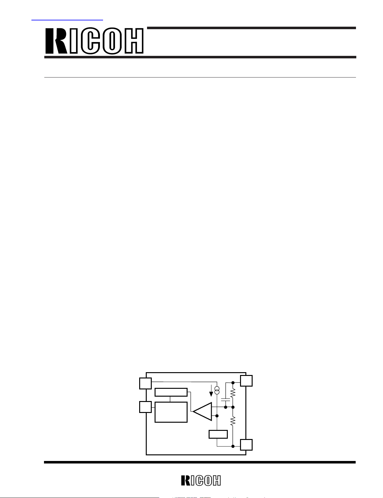
The RN5RY202 Series are VFM (chopper) Control ICs for step-up DC/DC converter with an external power transis-
tor featuring high output voltage accuracy and low supply current by CMOS process. Each of the RN5RY202
Series ICs consists of a voltage reference unit, an error amplifier, an oscillator, a VFM control circuit and feed back
resistors.
Output voltage is fixed at 2V in the IC.
A low ripple, high efficiency step-up DC/DC converter can be constructed by simply adding an inductor, a diode, a
capacitor, and a drive transistor and feed back resistors.
Although the series have no CE pins unlike RN5RY
××1A, high voltage (VOUT=30V) can be also output by using
external feed back resistors.
FEATURES
• Low Supply Current
............................................................................
TYP. 3µA
• Low Temperature-Drift Coefficient of Output Voltage
...................
TYP. ±50ppm/˚C
• High Accuracy Output Voltage
.........................................................
±2.5%
• Low Oscillation Start-up Voltage (no load)
......................................
MAX. 0.8V
• Any output voltage can be set with external resistors
• Small Package SOT-23-5 (Mini-Mold)
APPLICATIONS
• Constant voltage power source for battery-powered instruments.
• Constant power source for cameras, camcorders, pagers, and other hand-held communication tools.
• Constant power source for devices that require higher voltages than battery voltages.
BLOCK DIAGRAM
+
–
2
3
1
5
Vref
Oscillator
Output
Buffer
VOUT
VDD
GND
EXT
查询RN5RY202供应商
RN5RY202
2
SELECTION GUIDE
In the RN5RY202 Series, the taping type for the ICs can be selected at the user's request.
These selections can be made by designating the part number as shown below:
RN5RY202
×– ×× ←Part Number
↑↑↑ ↑
ab c d
{
{
Code Contents
a
20. Designation of Output Voltage (V
OUT)
V
OUT is fixed at 2.0V.
b2
Designation of Packing Type :
c A : Taping
C : Antistatic bag (for Samples only)
d
Designation of Taping Type :
Ex. TR, TL (refer to Taping Specifications ; TR type is prescribed as a standard.)
For example, Taping Type TR, is designated by Part Number RN5RY202A-TR.
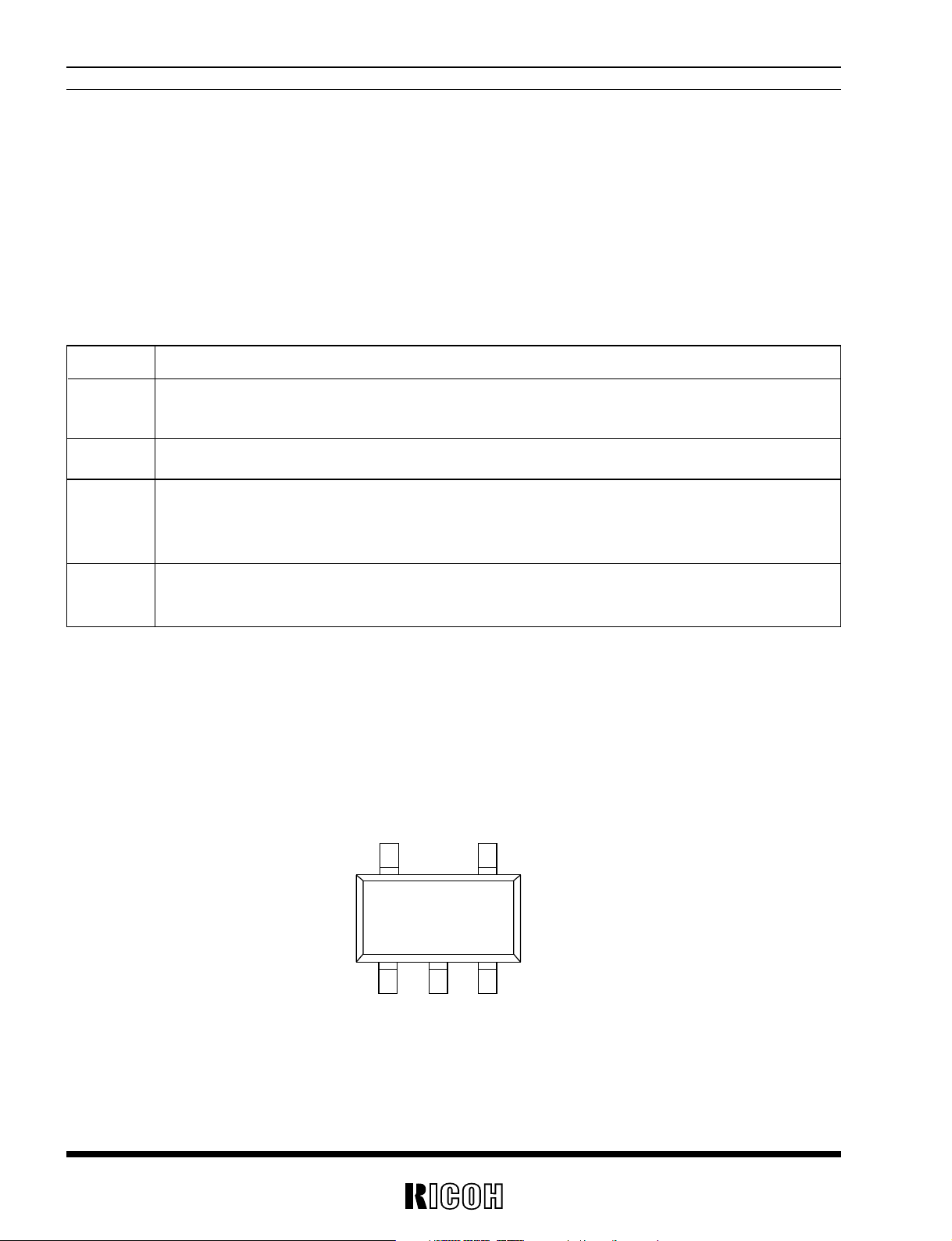
PIN CONFIGURATION
• SOT-23-5
12
3
54
mark side
RN5RY202
3
PIN DESCRIPTION
Pin No. Symbol Description
1 GND Ground Pin
2VDD Input Pin
3 EXT External Transistor Drive Pin (CMOS Output)
4 NC No Connection
5V
OUT Internal Voltage Output Pin (fixed at 2V)
ABSOLUTE MAXIMUM RATINGS
Symbol Item Ratings Unit
VDD Input Voltage 12 V
VOUT Output Pin Voltage 12 V
VEXT EXT Pin Output Voltage –0.3 to VDD+0.3 V
IEXT EXT Pin Output Current ±50 mA
PD Power Dissipation 150 mW
Topt Operating Temperature –40 to +85 ˚C
Tstg Storage Temperature –55 to +125 ˚C
Tsolder Lead Temperature (Soldering) 260˚C 10s (Lead part)
ABSOLUTE MAXIMUM RATINGS
Absolute Maximum ratings are threshold limit values that must not be exceeded even for an instant under
any conditions. Moreover, such values for any two items must not be reached simultaneously. Operation
above these absolute maximum ratings may cause degradation or permanent damage to the device. These
are stress ratings only and do not necessarily imply functional operation below these limits.
 Loading...