

RICOH RE5RL26AA-RR, RE5RL26AA-TZ, RE5RL26AC, RE5RL27AA-RF, RE5RL27AA-RR Datasheet
...
VOLTAGE REGULATOR
R×5RL SERIES
APPLICATION MANUAL
NO.EA-022-0006
VOLTAGE REGULATOR
R×5RL SERIES
1
OUTLINE
The R×5RL Series are voltage regulator ICs with high accuracy output voltage and ultra-low quiescent cur-
rent by CMOS process. Each of these ICs consists of a voltage reference unit, an error amplifier, a driver tran-
sistor, and resistors for setting output voltage. The output voltage is fixed with high accuracy.
Three types of packages, TO-92, SOT-89 (Mini-power Mold), SOT-23-5 (Mini-mold), are available.
• Ultra-low Quiescent Current
...........................
TYP. 1.1µA (R
×5RL30A, VIN=5.0V)
• Small Dropout Voltage
.....................................
TYP. 30mV (R
×5RL50A, IOUT=1mA)
• Low Temperature-Drift Coefficient of Output Voltage
...............
TYP. ±100 ppm/˚C
• Excellent Line Regulation
.................................
TYP. 0.1%/V
• Output Voltage
..................................................
Stepwise setting with a step of 0.1V in the range of 2.0V to 6.0V
is possible (refer to Selection Guide).
• High Accuracy Output Voltage
.........................
±2.5%
• Three Types of Packages
...................................
TO-92, SOT-89 (Mini-power Mold), SOT-23-5 (Mini-mold)
FEATURES
APPLICATIONS
• Power source for battery-powered equipment.
• Power source for cameras, video instruments such as camcorders, VCRs, and hand- held communication equipment.
• Precision voltage references.
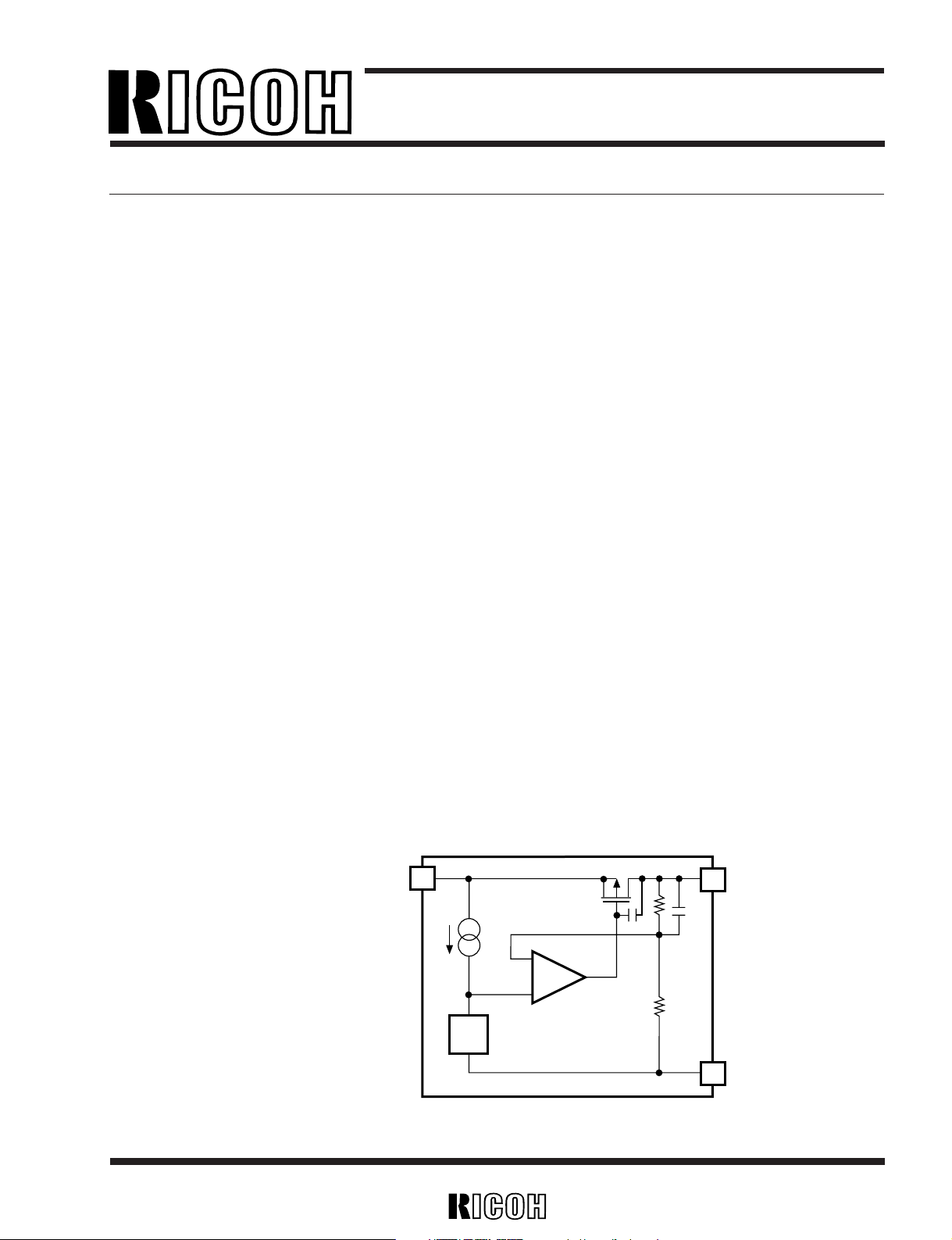
BLOCK DIAGRAM
2
1
3
Vref
V
OUT
GND
V
IN
–
+
1
R×5RL
2
SELECTION GUIDE
The package type, the output voltage, the packing type, and the taping type of R×5RL Series can be
designated at the user's request by specifying the part number as follows:
For example, the product with Package Type SOT-89, Output Voltage 5.0V, Version A,and Taping Type T1 are
designated by Part Number RH5RL50AA-T1.
Code Contents
Designation of Package Type:
a
E: TO-92
H: SOT-89 (Mini-power Mold)
N: SOT-23-5 (Mini-mold)
b
Setting Output Voltage (V
OUT):
Stepwise setting with a step of 0.1V in the range of 2.0V to 6.0V is possible.
cA
Designation of Packing Type:
d A: Taping
C: Antistatic bag for TO-92 and samples
Designation of Taping Type:
Ex. TO-92 : RF, RR, TZ
e
SOT-89 : T1, T2
SOT-23-5 : TR, TL
(refer to Taping Specifications)
“TZ”, “T1”, and “TR” are prescribed as standard directions.
R×5RL×××× – ×× ← Part Number
↑↑↑↑↑
abcde
}
}
R×5RL
3
•
TO-92
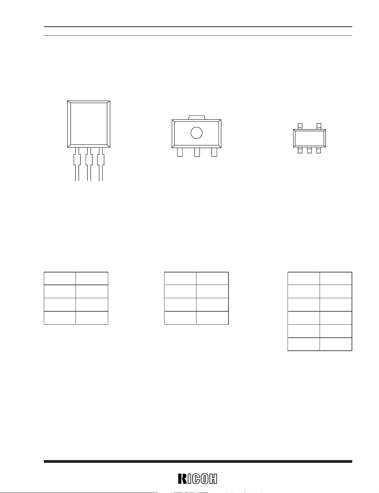
PIN CONFIGURATION
•
SOT-89
•
SOT-23-5
PIN DESCRIPTION
• TO-92 • SOT-89 • SOT-23-5
Pin No. Symbol
1 GND
2VIN
3VOUT
4NC
5NC
Pin No. Symbol
1 GND
2VIN
3VOUT
Pin No. Symbol
1 GND
2VIN
3VOUT
12
3
(mark side)
12
3
(mark side)
12
3
(mark side)
5
4
R×5RL
4
ABSOLUTE MAXIMUM RATINGS
Symbol Item
VIN Input Voltage
VOUT Output Voltage
IOUT Output Current
PD1 Power Dissipation 1 (NOTE1)
PD2 Power Dissipation 2 (NOTE2)
Topt Operating Temperature
Tstg Storage Temperature
Tsolder Lead Temperature (Soldering)
Rating Unit
+12 V
–0.3 to VIN +0.3 V
150 mA
300 mW
150 mW
– 40 to +85 ˚C
– 55 to +125 ˚C
260˚C,10s
Topt=25˚C
Absolute Maximum ratings are threshold limit values that must not be exceeded even for an instant under any
conditions. Moreover, such values for any two items must not be reached simultaneously. Operation above
these absolute maximum ratings may cause degradation or permanent damage to the device. These are stress
ratings only and do not necessarily imply functional operation below these limits.
ABSOLUTE MAXIMUM RATINGS
(NOTE 1) applied to SOT-89 and TO-92
(NOTE 2) applied to SOT-23-5
R×5RL
5
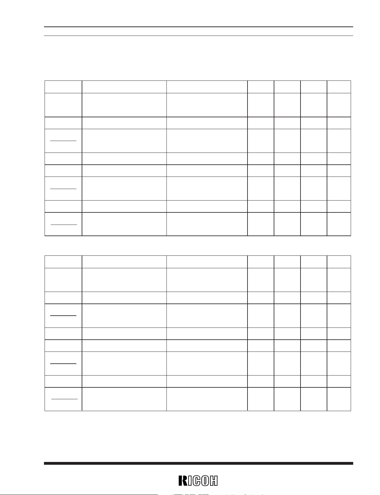
ELECTRICAL CHARACTERISTICS
• R×5RL20A
Symbol Item
VOUT Output Voltage
IOUT Output Current
∆V
OUT
Load Regulation
∆IOUT
VDIF Dropout Voltage
ISS Quiescent Current
∆V
OUT
∆VIN
Line Regulation
VIN Input Voltage
∆V
OUT Output Voltage
∆Topt Temperature Coefficient
Conditions MIN. TYP. MAX. Unit
VIN=4.0V
1.950 2.000 2.050 V
10
µA
≤IOUT≤10mA
VIN=4.0V 25 35 mA
V
IN=4.0V
1mA≤IOUT≤35mA
30 45 mV
IOUT=1mA 60 90 mV
VIN=4.0V 1.0 3.0
µ
A
I
OUT=1mA
VOUT+0.5V≤VIN≤10V
0.05 0.2 %/V
10 V
I
OUT=10mA
±100 ppm/˚C
–40˚C≤Topt≤85˚C
Topt=25˚C
• R×5RL30A
Topt=25˚C
Symbol Item
VOUT Output Voltage
IOUT Output Current
∆V
OUT
Load Regulation
∆
I
OUT
VDIF Dropout Voltage
ISS Quiescent Current
∆V
OUT
∆
V
IN
Line Regulation
VIN Input Voltage
∆V
OUT Output Voltage
∆
Topt Temperature Coefficient
Conditions MIN. TYP. MAX. Unit
VIN=5.0V
2.925 3.000 3.075 V
10µA≤IOUT≤10mA
VIN=5.0V 35 50 mA
V
IN=5.0V
1mA≤IOUT≤50mA
40 60 mV
IOUT=1mA 40 60 mV
VIN=5.0V 1.1 3.3 µA
I
OUT=1mA
VOUT
+
0.5V≤V
IN≤10V
0.05 0.2 %/V
10 V
I
OUT=10mA
±100 ppm/˚C
–40˚C≤Topt≤85˚C
 Loading...