

Ricoh RH5RH12B, RH5RH1A, RH5RH13B User Manual

ELECTRONIC DEVICES DIVISION
PWM STEP-UP DC/DC CONVERTER
RH5RH××1A/××2B/××3B SERIES
APPLICATION MANUAL
NO.EA-023-9803

NOTICE
1. The products and the product specifications described in this application manual are subject to change or discontinuation of production without notice for reasons such as improvement. Therefore, before deciding to use
the products, please refer to Ricoh sales representatives for the latest information thereon.
2. This application manual may not be copied or otherwise reproduced in whole or in part without prior written consent of Ricoh.
3. Please be sure to take any necessary formalities under relevant laws or regulations before exporting or otherwise taking out of your country the products or the technical information described herein.
4. The technical information described in this application manual shows typical characteristics of and example
application circuits for the products. The release of such information is not to be construed as a warranty of or a
grant of license under Ricoh's or any third party's intellectual property rights or any other rights.
5. The products listed in this document are intended and designed for use as general electronic components in
standard applications (office equipment, computer equipment, measuring instruments, consumer electronic
products, amusement equipment etc.). Those customers intending to use a product in an application requiring
extreme quality and reliability, for example, in a highly specific application where the failure or misoperation of
the product could result in human injury or death (aircraft, spacevehicle, nuclear reactor control system, traffic
control system, automotive and transportation equipment, combustion equipment, safety devices, life support
system etc.) should first contact us.
6. We are making our continuous effort to improve the quality and reliability of our products, but semiconductor
products are likely to fail with certain probability. In order prevent any injury to persons or damages to property
resulting from such failure, customers should be careful enough to incorporate safety measures in their design,
such as redundancy feature, fire-containment feature and fail-safe feature. We do not assume any liability or
responsibility for any loss or damage arising from misuse or inappropriate use of the products.
7. Anti-radiation design is not implemented in the products described in this application manual.
8. Please contact Ricoh sales representatives should you have any questions or comments concerning the products or the technical information.
June 1995

OUTLINE
......................................................................................................
1
FEATURES
....................................................................................................
1
APPLICATIONS
.............................................................................................
1
BLOCK DIAGRAM
.........................................................................................
2
SELECTION GUIDE
.......................................................................................
2
PIN CONFIGURATION
...................................................................................
3
PIN DESCRIPTION
........................................................................................
3
ABSOLUTE MAXIMUM RATINGS
...................................................................
4
ELECTRICAL CHARACTERITICS
...................................................................
5
OPERATION OF STEP-UP DC/DC CONVERTER
...........................................
10
TYPICAL CHARACTERISTICS
......................................................................
13
1) Output Voltage vs. Output Current
.......................................................................
13
2) Efficiency vs. Output Current
.............................................................................
14
3) Supply Current (No Load) vs. Input Voltage
..............................................................
15
4) Output Current vs. Ripple Voltage
........................................................................
15
5) Start-up/Hold-on Voltage vs. Output Current (Topt=25˚C)
...............................................
16
6) Output Voltage vs. Temperature
.........................................................................
17
7) Start-up Voltage vs. Temperature
........................................................................
18
8) Hold-on Voltage vs. Temperature
........................................................................
18
9) Supply Current 1 vs. Temperature
.......................................................................
18
10) Supply Current 2 vs. Temperature
.......................................................................
18
11) Lx Switching Current vs. Temperature
...................................................................
18
12) Lx Leakage Current vs. Temperature
....................................................................
18
13) Oscillator Frequency vs. Temperature
....................................................................
19
14) Oscillator Duty Cycle vs. Temperature
...................................................................
19
15) Vlx Voltage Limit vs. Temperature
........................................................................
20
16) EXT “H” Output Current vs. Temperature
................................................................
20
17) EXT “L” Output Current vs. Temperature
.................................................................
20
18) Load Transient Response
................................................................................
21
19) Distribution of Output Voltage
............................................................................
22
20) Distribution of Oscillator Frequency
......................................................................
22
RH5RH SERIES
APPLICATION MANUAL
CONTENTS

TYPICAL APPLICATIONS
............................................................................
23
• RH5RH××1A
.................................................................................................
23
• RH5RH××2B
..................................................................................................
23
• RH5RH××3B
..................................................................................................
24
• CE pin Drive Circuit
............................................................................................
22
APPLICATION CIRCUITS
.............................................................................
26
• 12V Step-up Circuit
............................................................................................
26
• Step-down Circuit
..............................................................................................
26
• Step-up/Step-down Circuit with Flyback
.......................................................................
27
PACKAGE DIMENSIONS
..............................................................................
28
TAPING SPECIFICATIONS
...........................................................................
28

PWM STEP-UP DC/DC CONVERTER
1
RH5RH
××
1A/
××
2B/
××
3B SERIES
OUTLINE
The RH5RH××1A/××2B/××3B Series are PWM Step-up DC/DC converter ICs by CMOS process.
The RH5RH
××1A IC consists of an oscillator, a PWM control circuit, a driver transistor (Lx switch), a refer-
ence voltage unit, an error amplifier, a phase compensation circuit, resistors for voltage detection, a soft-start circuit, and an Lx switch protection circuit. A low ripple, high efficiency step-up DC/DC converter can be constructed
of this RH5RH
××1A IC with only three external components, that is, an inductor, a diode and a capacitor.
These RH5RH
××1A/××2B/××3B ICs can achieve ultra-low supply current (no load) –TYP. 15µA –by a new-
ly developed PWM control circuit, equivalent to the low supply current of a VFM (chopper) Step-up DC/DC converter.
Furthermore, these ICs can hold down the supply current to TYP. 2µA by stopping the operation of the oscil-
lator when the input voltage > (the output voltage set value + the dropout voltage by the diode and the inductor).
These RH5RH
××1A/××2B/××3B Series ICs are recommendable to the user who desires a low ripple PWM
DC/DC converter, but cannot adopt a conventional PWM DC/DC converter because of its too large supply current.
The RH5RH
××2B/××3B Series ICs use the same chip as that employed in the RH5RH××1A IC and are pro-
vided with a drive pin (EXT) for an external transistor. Because of the use of the drive pin (EXT), an external
transistor with a low saturation voltage can be used so that a large current can be caused to flow through the
inductor and accordingly a large output current can be obtained. Therefore, these RH5RH
××2B/××3B Series ICs
are recommendable to the user who need a current as large as several tens mA to several hundreds mA.
The RH5RH
××3B IC also includes an internal chip enable circuit so that it is possible to set the standby sup-
ply current at MAX. 0.5µA.
These RH5RH
××1A/××2B/××3B ICs are suitable for use with battery-powered instruments with low noise
and low supply current.
•
Small Number of External Components
..........
Only an inductor, a diode and a capacitor (RH5RH××1A)
•
Low Supply Current
...........................................
TYP. 15µA (RH5RH301A)
•
Low Ripple and Low Noise
•
Low Start-up Voltage (when the output current is 1mA)
..................
MAX. 0.9V
•
High Output Voltage Accuracy
..........................
±2.5%
•
High Efficiency
...................................................
TYP. 85%
•
Low Temperature-Drift Coefficient of Output Voltage
......................
TYP. ±50 ppm/˚C
•
Soft-Start
.............................................................
MIN. 500µs
•
Small Packages
...................................................
SOT-89 (RH5RH××1A, RH5RH××2B),
SOT-89-5 (RH5RH
××
3B)
FEATURES
APPLICATIONS
•
Power source for battery-powered equipment.
•
Power source for cameras, camcorders, VCRs, PDAs, electronic data banks,and hand-held communication
equipment.
•
Power source for instruments which require low noise and low supply current, such as hand-held audio equip-
ment.
•
Power source for appliances which require higher cell voltage than that of batteries used in the appliances.
2
RH5RH
×××× – ×× ← Part Number
↑ ↑ ↑
a b c
SELECTION GUIDE
In RH5RH Series, the output voltage, the driver, and the taping type for the ICs can be selected at the user's
request. The selection can be made by designating the part number as shown below :
For example, the product with Output Voltage 5.0V, the External Driver (the Oscillator Frequency 100kHz)
and Taping Type T1, is designated by Part Number RH5RH502B-T1.
Code Description
Setting Output Voltage (VOUT):
a
Stepwise setting with a step of 0.1V in the range of 2.7V to 7.5V is possible.
Designation of Driver:
1A: Internal Lx Tr. Driver (Oscillator Frequency 50kHz)
b 2B: External Tr. Driver (Oscillator Frequency 100kHz)
3B: Internal Tr./External Tr. (selectively available) (Oscillator Frequency 100kHz, with chip
enable function)
Designation of Taping Type :
c
Ex. SOT-89 :T1, T2
SOT-89-5 :T1, T2
(refer to Taping Specifications)
“T1” is prescribed as a standard.
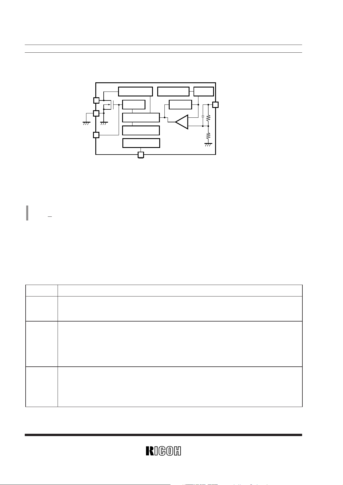
RH5RH
BLOCK DIAGRAM
Lx
Vss
EXT
LxSW
CE
Error Amp.
OUT
V
LX limiter
Buffer
PWM control
OSC
Chip Enable
Slow start
Phase Comp.
Vref
+
–
Error Amp. (Error Amplifier) has a DC gain of 80dB, and Phase Comp. (Phase Compensation Circuit)
provides the frequency characteristics including the 1st pole (fp=0.25Hz) and the zero point (fz=2.5kHz).
Furthermore, another zero point (fz=1.0kHz) is also obtained by the resistors and a capacitor connected to
the OUT pin.
(Note) Lx Pin
............
only for RH5RH××1A and RH5RH××3B
EXT Pin
.........
only for RH5RH
××2B and RH5RH××3B
CE Pin
...........
only for RH5RH
××3B
}
}
}
3
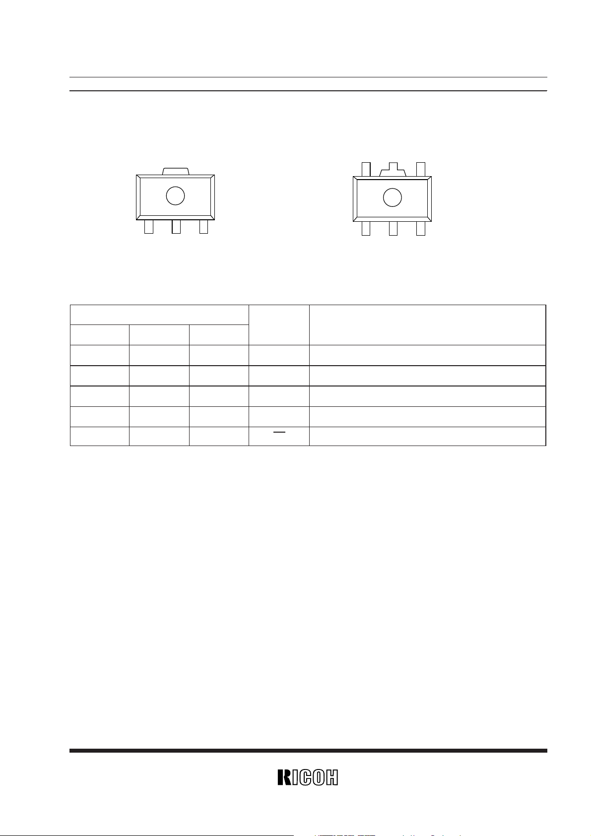
•
SOT-89-5
PIN CONFIGURATION
•
SOT-89
PIN DESCRIPTION
Pin No.
××1B ××2B ××3B
1 1 5
2 2 2
3 — 4
— 3 3
— — 1
RH5RH
Symbol Description
VSS Ground Pin
OUT Step-up Output Pin, Power Supply (for device itself)
Lx Switching Pin (Nch Open Drain)
EXT External Tr. Drive Pin (CMOS Output)
CE Chip Enable Pin (Active Low)
5
4
(mark side)
1 2
(mark side)
3
1 2
3
4
RH5RH
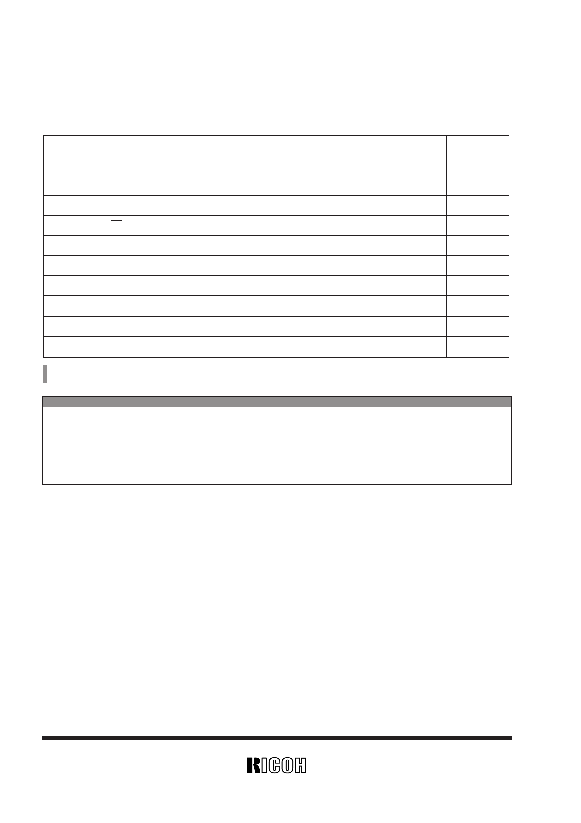
ABSOLUTE MAXIMUM RATINGS
Symbol Item
VOUT Output Pin Voltage
VLX Lx Pin Voltage
VEXT EXT Pin Voltage
VCE CE Pin Voltage
ILX Lx Pin Output Current
IEXT EXT Pin Current
PD Power Dissipation
Topt Operating Temperature Range
Tstg Storage Temperature Range
Tsolder Lead Temperature(Soldering)
Rating Unit Note
+12 V
+12 V Note1
– 0.3 to VOUT+0.3 V Note2
–0.3 to VOUT+0.3 V Note3
250 mA Note1
±50 mA Note2
500 mW
–30 to +80 ˚C
–55 to +125 ˚C
260˚C,10s
(Note 1) Applicable to RH5RH××1A and RH5RH××3B. (Note 2) Applicable to RH5RH××2B and RH5RH××3B.
(Note 3) Applicable to RH5RH
××3B.
Vss=0V
Absolute Maximum ratings are threshold limit values that must not be exceeded even for an instant under any
conditions. Moreover, such values for any two items must not be reached simultaneously. Operation above
these absolute maximum ratings may cause degradation or permanent damage to the device. These are stress
ratings only and do not necessarily imply functional operation below these limits.
ABSOLUTE MAXIMUM RATINGS
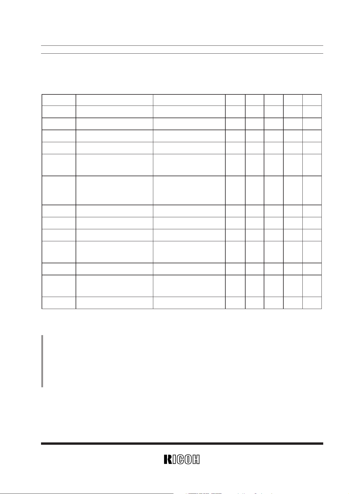
5
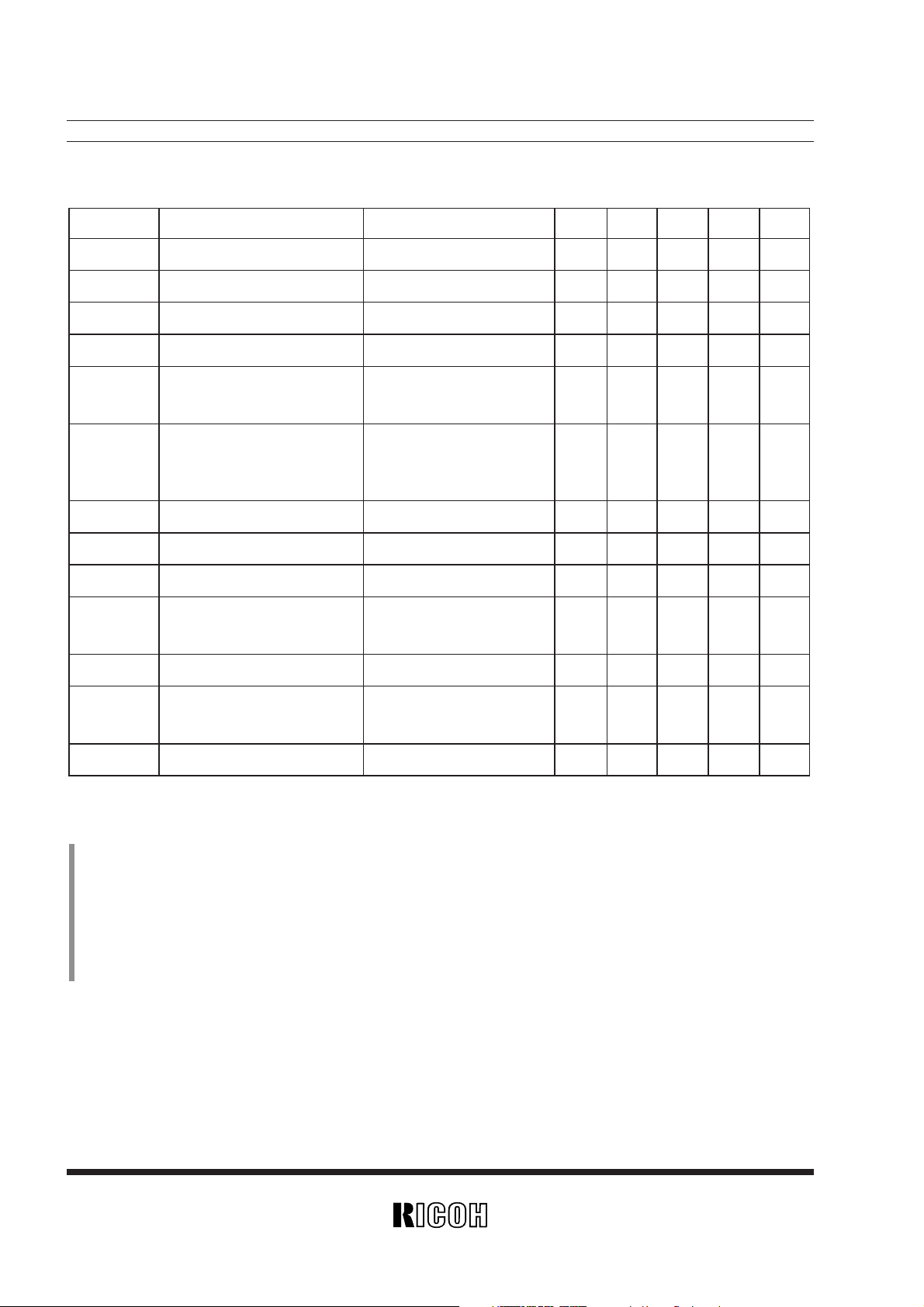
ELECTRICAL CHARACTERISTICS
• RH5RH301A
Symbol Item
VOUT Output Voltage
VIN Input Voltage
Vstart Start-up Voltage
Vhold Hold-on Voltage
I
DD1 Supply Current 1
IDD2 Supply Current 2
ILX Lx Switching Current
ILXleak Lx Leakage Current
fosc Oscillator Frequency
Maxdty
Oscillator Maximum Duty
Cycle
η
Efficiency
tstart Soft-Start Time
VLXlim VLX Voltage Limit
Conditions MIN. TYP. MAX. Unit Note
2.925 3.000 3.075 V
8 V
IOUT=1mA,V
IN : 0→2V 0.8 0.9 V
IOUT=1mA,VIN : 2→0V 0.7 V
To be measured at OUT Pin
(excluding Switching Current)
15 25 µA
To be measured at OUT Pin
(excluding Switching Current) 2 5 µA
VIN=3.5V
VLX=0.4V 60 mA
VLX=6V,VIN=3.5V 0.5 µA
40 50 60 kHz
on (VLX “L” ) side 70 80 90 %
70 85 %
Time required for the rising
0.5 2.0 ms Note1
of VOUT up to 3V.
Lx Switch ON 0.65 0.8 1.0 V Note2
VOUT=3.0V
RH5RH
Unless otherwise provided, VIN=1.8V, VSS=0V, IOUT=10mA, Topt=25˚C, and use External Circuit of Typical
Application (FIG. 1).
(Note 1) Soft-Start Circuit is operated in the following sequence :
(1) V
IN is applied.
(2) The voltage (Vref) of the reference voltage unit is maintained at 0V for about 200µs after the application of V
IN.
(3) The output of Error Amp. is raised to “H” level during the maintenance of the voltage (Vref) of the reference voltage unit.
(4) After the rise of Vref, the output of Internal Error Amp. is gradually decreased to an appropriate value by the function of Internal Phase
Compensation Circuit, and the Output Voltage is gradually increased in accordance with the gradual decrease of the output of Internal Error
Amp.
(Note 2) I
LX is gradually increased after Lx Switch is turned ON. In accordance with the increase of ILX, VLX is also increased. When VLX reaches VLXlim,
Lx Switch is turned OFF by an Lx Switch Protection Circuit.
6
RH5RH
• RH5RH501A
VOUT=5.0V
Unless otherwise provided, VIN=3V, Vss=0V, IOUT=10mA, Topt=25˚C, and use External Circuit of Typical
Application (FIG. 1).
(Note 1) Soft-Start Circuit is operated in the following sequence :
(1) V
IN is applied.
(2) The voltage (Vref) of the reference voltage unit is maintained at 0V for about 200µs after the application of V
IN.
(3) The output of Error Amp. is raised to “H” level during the maintenance of the voltage (Vref) of the reference voltage unit.
(4) After the rise of Vref, the output of Internal Error Amp. is gradually decreased to an appropriate value by the function of Internal Phase
Compensation Circuit, and the Output Voltage is gradually increased in accordance with the gradual decrease of the output of Internal Error
Amp.
(Note 2) I
LX is gradually increased after Lx Switch is turned ON. In accordance with the increase of ILX, VLX is also increased. When VLX reaches VLXlim,
Lx Switch is turned OFF by an Lx Switch Protection Circuit.
Symbol Item
VOUT Output Voltage
VIN Input Voltage
Vstart Start-up Voltage
Vhold Hold-on Voltage
I
DD
1 Supply Current 1
IDD2 Supply Current 2
ILX Lx Switching Current
ILXleak Lx Leakage Current
fosc Oscillator Frequency
Maxdty
Oscillator Maximum Duty
Cycle
η
Efficiency
tstart Soft-Start Time
VLXlim VLX Voltage Limit
Conditions MIN. TYP. MAX. Unit Note
4.875 5.000 5.125 V
8 V
Iout=1mA,Vin:0→2V 0.8 0.9 V
Iout=1mA,Vin:2→0V 0.7 V
To be measured at OUT Pin
(excluding Switching Current)
30 45 µA
To be measured at OUT Pin
(excluding Switching Current) 2 5 µA
VIN=5.5V
VLX=0.4V 80 mA
VLX=6V,VIN=5.5V 0.5 µA
40 50 60 kHz
on (VLX “L” ) side 70 80 90 %
70 85 %
Time required for the rising
0.5
2.0
ms Note1
of VOUT up to 5V.
Lx Switch ON 0.65 0.8 1.0 V Note2
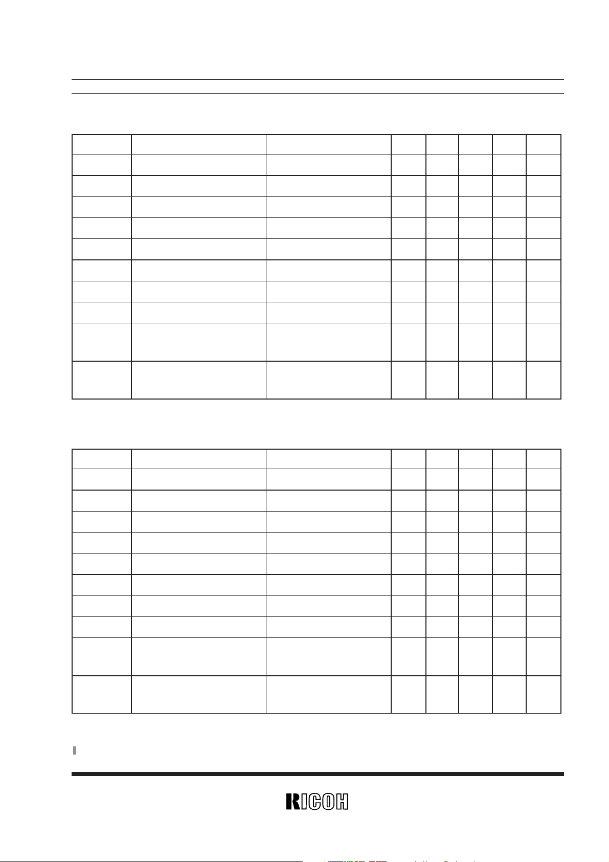
7
RH5RH
• RH5RH302B
Symbol Item
VOUT Output Voltage
VIN Input Voltage
Vstart Oscillator Start-up Voltage
IDD
1
Supply Current 1
IDD
2
Supply Current 2
IEXTH EXT “H” Output Current
IEXTL EXT “L” Output Current
fosc Oscillator Frequency
Maxdty
Oscillator Maximum Duty
Cycle
tstart Soft-Start Time
Conditions MIN. TYP. MAX. Unit Note
2.925 3.000 3.075 V
8 V
EXT no load,VOUT :0→2V 0.7 0.8 V
EXT no load,VOUT=2.88V 30 50 µA
EXT no load,VOUT=3.5V 2 5 µA
VEXT=V
OUT–0.4V –1.5 mA
VEXT=0.4V 1.5 mA
80 100 120 kHz
VEXT “H” side
70 80 90
%
Time required for the rising
0.5
2.0
ms Note1
of V
OUT up to 3V
VOUT=3.0V
Unless otherwise provided, VIN=1.8V, Vss=0V, IOUT=10mA, Topt=25˚C, and use External Circuit of Typical
Application (FIG. 2).
• RH5RH502B
VOUT=5.0V
Unless otherwise provided, VIN=3V, Vss=0V, IOUT=10mA, Topt=25˚C and use External Circuit of Typical
Application (FIG. 2).
(Note 1) refer to page 5 (Note 1)
Symbol Item
VOUT Output Voltage
VIN Input Voltage
Vstart Oscillator Start-up Voltage
IDD
1
Supply Current 1
IDD
2
Supply Current 2
IEXTH EXT “H” Output Current
IEXTL EXT “L” Output Current
fosc Oscillator Frequency
Maxdty
Oscillator Maximum Duty
Cycle
t
start Soft-Start Time
Conditions MIN. TYP. MAX. Unit Note
4.875 5.000 5.125 V
8 V
EXT no load,VOUT :0→2V 0.7 0.8 V
EXT no load,VOUT=4.8V 60 90 µA
EXT no load,VOUT=5.5V 2 5 µA
VEXT=VOUT–0.4V –2 mA
VEXT=0.4V 2 mA
80 100 120 kHz
VEXT “H” side
70 80 90 %
Time required for the rising
0.5 2.0 ms Note1
of V
OUT up to 5V
 Loading...