RICOH RF5C15, RJ5C15, RP5C15 Datasheet

DISCONTINUED
REAL-TIME CLOCK
1
RP/RF/RJ5C15
OUTLINE
The RP/RF/RJ5C15 are real-time clocks for microcomputers that can be connected directly to data buses of
16bit CPUs, such as the 8086, Z8000, and 68000, and of 8bit CPUs, such as the 8085A, Z80, 6809, and 6502. They
allow setting or reading of the clock with the same procedures as for the Read/Write operation for memory.
These products have various features including clock, calendar and alarm functions and can be backed up by
batteries.
• Connected directly to CPU enabling fast access. • 4bit bidirectional data bus : D0 - D3
• 4bit address input : A0 - A3
• Built-in clock counter (hour, minute, second) and calendar counter (leap year, year, month, day, day-of-the-week)
• All clock data expressed in BCD codes
• Backed up by batteries (minimum : 2.0V)
• Selectable basic clock frequency : 16kHz, 1kHz, 128Hz, 16Hz, 1Hz, 1/60Hz.
• Outputs alarm signals or timing pulse of 16Hz or 1Hz. • CMOS technology
• Supply voltage : Single power supply of +5V
• Packages RP5C15
......
18pin DIP
RF5C15
......
18pin SOP
RJ5C15
......
28pin PLCC
FEATURES
NO. EK-086-9908
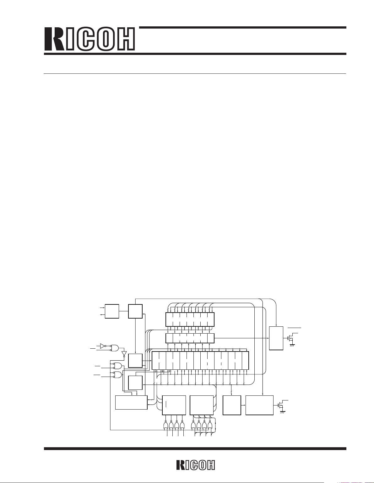
BLOCK DIAGRAM
S1 S2 S3 S4 S5 S6 S7 S8 S9 SA SB
SC
OSCIN
OSCOUT
CS
CS
RD
WR
OSC 1/2
15
16kHz, 1kHz, 128Hz, 16Hz, 1Hz, 1/60Hz 1Hz, 16Hz
T.RESET
RD.WR.
BANK 1
ALARM
RESET
RD. WR.
ALARM
ALARM
OUTPUT
BANK 0. RD. WR.
CLOCK
HOLD
ADJ
HOLD
CONTROLLER
SO
SF
ADDRESS
DECODER
BUS
CONTROL
CLOCK
SELECT
CLOCK
OUTPUT
CLKOUT
ALARM
3
SD
-SF
4
4 3434234241442
S0
SECONDS MINUTES HOURS DAYS MONTHS YEARS
WEEK
LEAP
YEARS
COMPARATOR
ALARM REGISTER
4342342
S2 S3S4S5 S6 S7 S8
A0A1A2A3 D0D1D2D3
1
/101/61/101/61/121/241/7
1
/101/101/4
1
/28-1/311/12

RP/RF/RJ5C15
2
DISCONTINUED
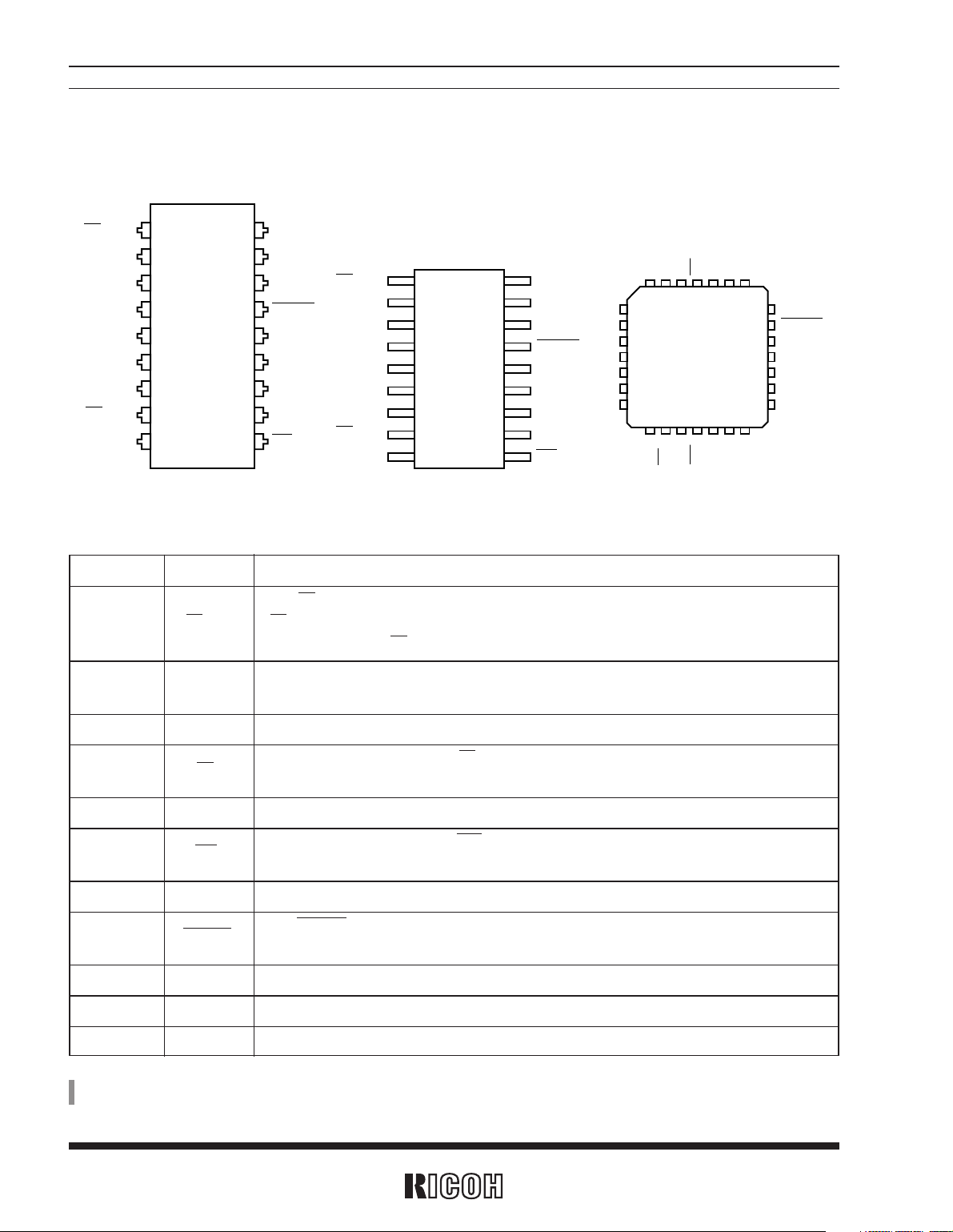
PIN CONFIGURATIONS
CS
CS
CLKOUT
A0
A1
A2
A3
RD
GND
VCC
OSCOUT
OSCIN
ALARM
D3
D2
D1
D0
WR
CS
CS
CLKOUT
A
0
A1
A2
A3
RD
GND
VCC
OSCOUT
OSCIN
ALARM
D
3
D2
D1
D0
WR
NC
A0
NC
A1
NC
A2
NC
NC
CLKOUTCSCS
Vcc
OSCOUT
OSCIN
NC
ALARM
NC
D3
NC
D2
NC
5
6
7
8
9
10
11
25
24
23
22
21
20
19
12131415161718
4 3 2 1 282726
A3RDGNDWRNC
D0D1
1
2
3
4
5
6
7
8
9
18
17
16
15
14
13
12
11
10
1
2
3
4
5
6
7
8
9
18
17
16
15
14
13
12
11
10
• RP5C15 (18pin DIP) • RF5C15 (18pin SOP) • RJ5C15 (28pin PLCC)
PIN DESCRIPTION
*
) Pin numbers shown are for the RP5C15 and the RF5C15. These are different for the RJ5C15.
For specific pin number see the “PIN CONFIGURATIONS”.
Pin No. Symbol Function
1,2 CS, CS
The CS and CS are used to interface with external devices. Enabled when CS =“H” and
CS=“L”. The CS is connected to the power down detector in the system power supply
assembly while the CS is connected to the microcomputer.
3 CLKOUT
Output pin for reference clock pulse and an open drain output. Selectable from 8 modes
based on the setting of the clock select register as shown in the separate table.
4,5,6,7 A0 to A3 Input pins for the address signal. These pins are connected to the CPU address bus.
8 RD
Input pin for I/O control. The RD is set to “L” when data is transferred from the
RP/RF/RJ5C15 to the CPU.
9 GND Ground pin for the power supply of 0V.
10 WR
Input pin for I/O control. The WR is set to “L” when data is transferred from the CPU to
the RP/RF/RJ5C15.
11,12,13,14 D0 to D3 Bidirectional data bus. Connected to the data bus of the CPU.
15 ALARM
The ALARM outputs alarm signal and 16Hz and 1Hz clock pulses. This pin is an open
drain output.
16 OSCIN The OSCIN and OSCOUT are connected to the 32.768kHz crystal oscillator.
17 OSCOUT 32.768kHz
18 V
CC Input pin for the power supply of +5V.

DISCONTINUED
Absolute Maximum ratings are threshold limit values that must not be exceeded even for an instant under
any conditions. Moreover, such values for any two items must not be reached simultaneously. Operation
above these absolute maximum ratings may cause degradation or permanent damage to the device. These
are stress ratings only and do not necessarily imply functional operation below these limits.
RP/RF/RJ5C15
3
ABSOLUTE MAXIMUM RATINGS
RECOMMENDED OPERATING CONDITIONS
Symbol Item Conditions Ratings Unit
VCC Supply Voltage –0.3 to 7.0 V
VI Input Voltage –0.3 to VCC+0.3 V
VO Output Voltage –0.3 to VCC+0.3 V
Pd Maximum Power Dissipation Ta=25˚C 400 mW
Topr Operating Temperature –20 to 70 ˚C
Tstg Storage Temperature –40 to 125 ˚C
Symbol Item Conditions MIN. TYP. MAX. Unit
VCC Supply Voltage 4.5 5 5.5 V
VDH Data Preservation Voltage 2.0 5.5 V
fXT Crystal Oscillation Frequency 32.768 kHz
Referenced at GND pin
(Unless otherwise specified, Ta=–20 to 70˚C)
ABSOLUTE MAXIMUM RATINGS

RP/RF/RJ5C15
4
DISCONTINUED
DC ELECTRICAL CHARACTERISTICS
Symbol Item Conditions MIN. TYP. MAX. Unit
VIH
“H” Input Voltage (excluding OSCIN) 2.0
Vcc+0.3
V
“H” Input Voltage (OSCIN) 2.4
Vcc+0.3
V
VIL
“L” Input Voltage (excluding OSCIN) –0.3 0.8 V
“L” Input Voltage (OSCIN) –0.3 0.5 V
VOH “H” Output Voltage IOH=–400µA 2.4 V
VOL “L” Output Voltage IOL=2mA 0.4 V
ILI Input Leakage Current VIN=0 to Vcc –10 10 µA
IOZ Output Off-state Leakage Current Voz=0 to 5.5V ±10 µA
ICC1 Supply Current for Backup fXT=32.768kHz, Vcc=2.0V 15 µA
ICC2 Operating Supply Current fXT=32.768kHz, Vcc=5.5V* 250 µA
VILCS CS pin “L” Input Voltage for Backup Vcc=2.0V –0.2 0.2 V
V
IHCS CS pin “H” Input Voltage for Backup Vcc=2.0V 1.8 2.0 V
(Unless otherwise specified, Ta=–20 to 70˚C, Vcc=5V±10%)
*
) RD, WR signal frequency : 100kHz ; Input pin is fixed at Vcc or GND level ; output pin open.
AC ELECTRICAL CHARACTERISTICS
Symbol Item Conditions MIN. TYP. MAX. Unit
tAC Address–RD/WR Delay Time 50 ns
tcc RD/WR Pulse Width 120 13000 ns
tCA
Address Effective Time after rising
10 ns
of RD/WR
tRD Data Delay Time after falling of RD 1TTL+100pF 120 ns
tRDH Data Hold Time after rising of RD 10 ns
tWDS Data Setup Time in Write operation 100 ns
tWDH Data Hold Time in Write operation 20 ns
tTED Timer Enable to Timer Disable 100 µs
tADJ Adjust Completion Time 100 µs
tAINH
Alarm Write Inhibit Time after Resetting
100 µs
tRCV RD/WR Recovery Time 1 µs
(Unless otherwise specified, Ta=–20 to 70˚C, Vcc=5V±10%)
 Loading...