RICOH RF5C01A, RP5C01A Datasheet

REAL-TIME CLOCK
WITH INTERNAL RAM
1
RP/RF5C01A
OUTLINE
The RP/RF5C01A are real-time clocks for microcomputers that can be connected directly to buses of microcomputers with such CPUs as the 8085A or Z80 and allow setting or reading of the clock with the same procedures as
for the Read/Write operation for memory.
These products have various features such as clock and calendar counters, alarm functions, and 26
´ 4bits RAM
which can be backed up by batteries. They can then be used as non-volatile RAM.
• Connected directly to CPU • 4bit bidirectional data bus : D0 - D3 • 4bit address input : A0 - A3
• Built-in clock counter (hour, minute, second) and calendar counter (leap year, year, month, day, day-of-the-week)
• Supports both 12-hour AM/PM clock and 24-hour clock
• All clock data expressed in BCD codes • ±30 second adjustment function
• Backed up by batteries (minimum:2.2V) • Built-in 26
´ 4bits RAM
• Outputs alarm signals or timing pulse of 16Hz or 1Hz.
• Packages : 18pin DIP (RP5C01A) ; 18pin SOP(RF5C01A)
FEATURES
NO. EK-086-9804
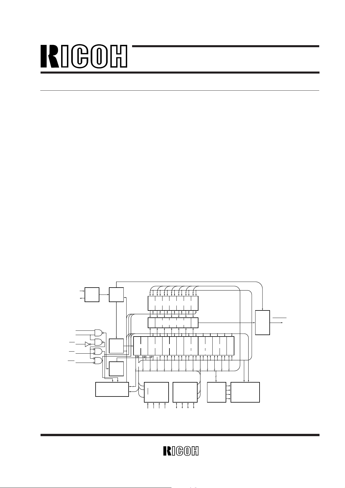
BLOCK DIAGRAM
S1 S2 S3 S4 S5 S6 S7 S8 S9 SA SB
SC
OSCIN
OSCOUT
CS
CS
WR
RD
ADJ
OSC 1/2
15
1Hz,16Hz,
T-RESET
RD.WR.
MODE01
A-RESET
RD. WR.
MODE 00
ALARM
ALARM
OUTPUT
RD.WR.
MODE10,MODE11
CLOCK
HOLD
ADJ
HOLD
CONTROLLER
SO
SF
ADDRESS
DECODER
BUS
CONTROL
INTERNAL
BUS
BUFFER
26´4bits
RAM
ALARM
4
SO-SC
SD
-SF
4
43434234241442
S0
SECONDS MINUTES HOURS DAYS MONTHS YEARS
WEEK
LEAP
YEARS
COMPARATOR
ALARM REGISTER
4342342
S2 S3 S4 S5 S6 S7 S8
A0A1A2A3 D0D1D2D3
1
/101/61/101/61/121/241/7
1
/101/101/4
1
/28-1/311/12

RP/RF5C01A
2
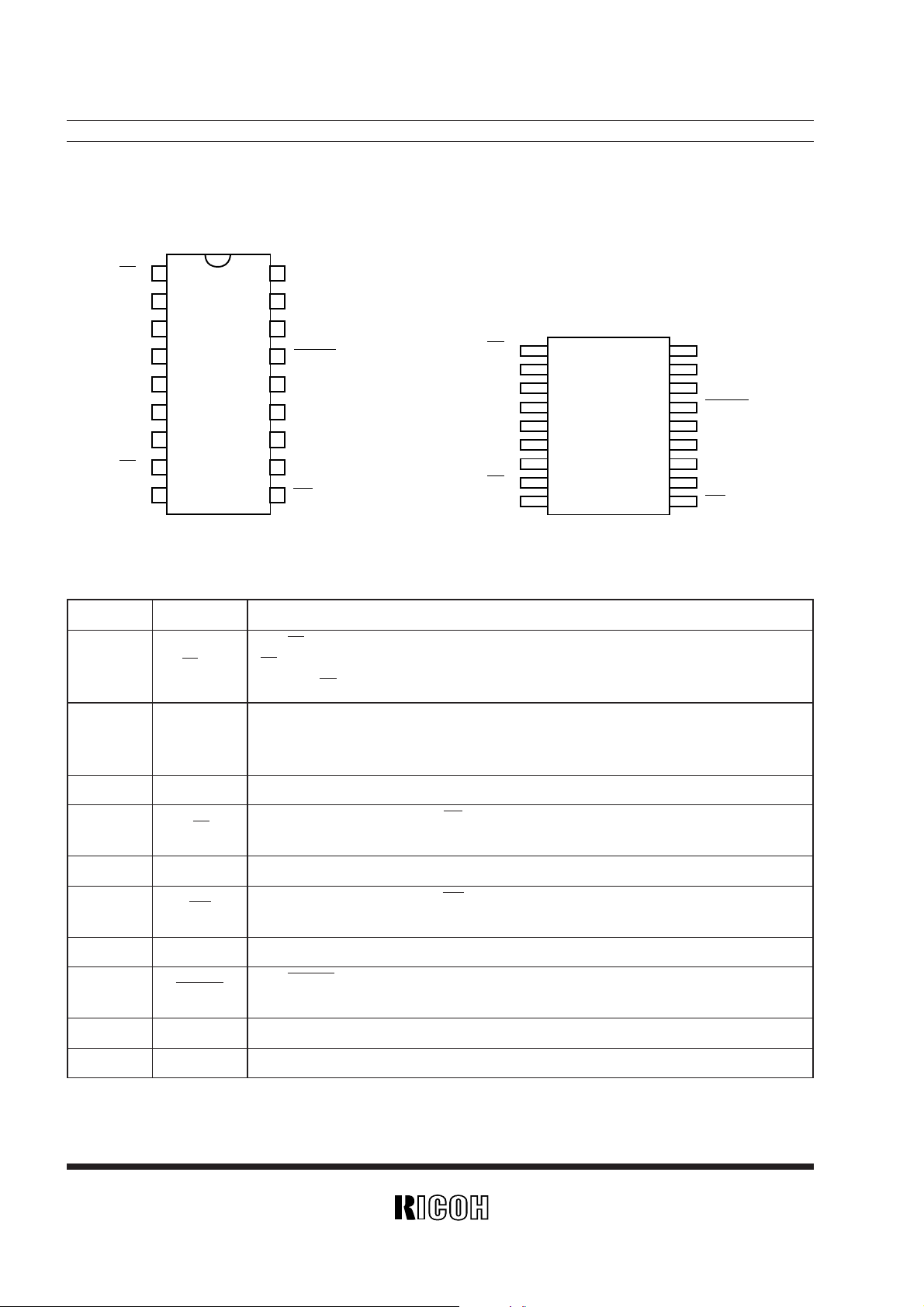
PIN CONFIGURATIONS
CS
CS
ADJ
A0
A
1
A2
A3
RD
GND
18
17
16
15
14
13
12
11
10
Vcc
OSCOUT
OSCIN
ALARM
D
3
D2
D1
D0
WR
1
2
3
4
5
6
7
8
9
CS
CS
ADJ
A
0
A1
A2
A3
RD
GND
18
17
16
15
14
13
12
11
10
Vcc
OSCOUT
OSCIN
ALARM
D
3
D2
D1
D0
WR
1
2
3
4
5
6
7
8
9
• RP5C01A • RF5C01A
PIN DESCRIPTION
Pin No. Symbol Function
1,2 CS,CS
The CS and CS are used to interface with external devices. Enabled when CS =“H” and
CS=“L”. The CS is connected to the power down detector in the system power supply
while the CS is connected to the microcomputer.
3 ADJ
The ADJ can easily correct seconds without using the CPU. When this pin is set to “H” the
second digits ranging from 00 to 29 are set to 0, the second digits ranging from 30 to 59 are
set to 0 and minute digits are incremented by 1.
4,5,6,7 A0 to A3 Input pin for the address signal. These pins are connected to the CPU address bus.
8 RD
Input pin for I/O control. The RD is set to “L” when data is transferred from the
RP/RF5C01A to the CPU.
9 GND Ground pin for the power supply of 0V.
10 WR
Input pin for I/O control. The WR is set to “L” when data is transferred from the CPU to
the RP/RF5C01A.
11,12,13,14 D0 to D3 Bidirectional data bus. Connected to the data bus of the CPU.
15 ALARM
The ALARM pin outputs alarm signals and 16Hz and 1Hz clock pulses.
This pin is an open drain output.
16,17
OSCIN,OSCOUT
The OSCIN and OSCOUT are connected to the crystal oscillator of 32.768kHz
18 V
CC Input pin for the power supply of +5V.

RP/RF5C01A
3
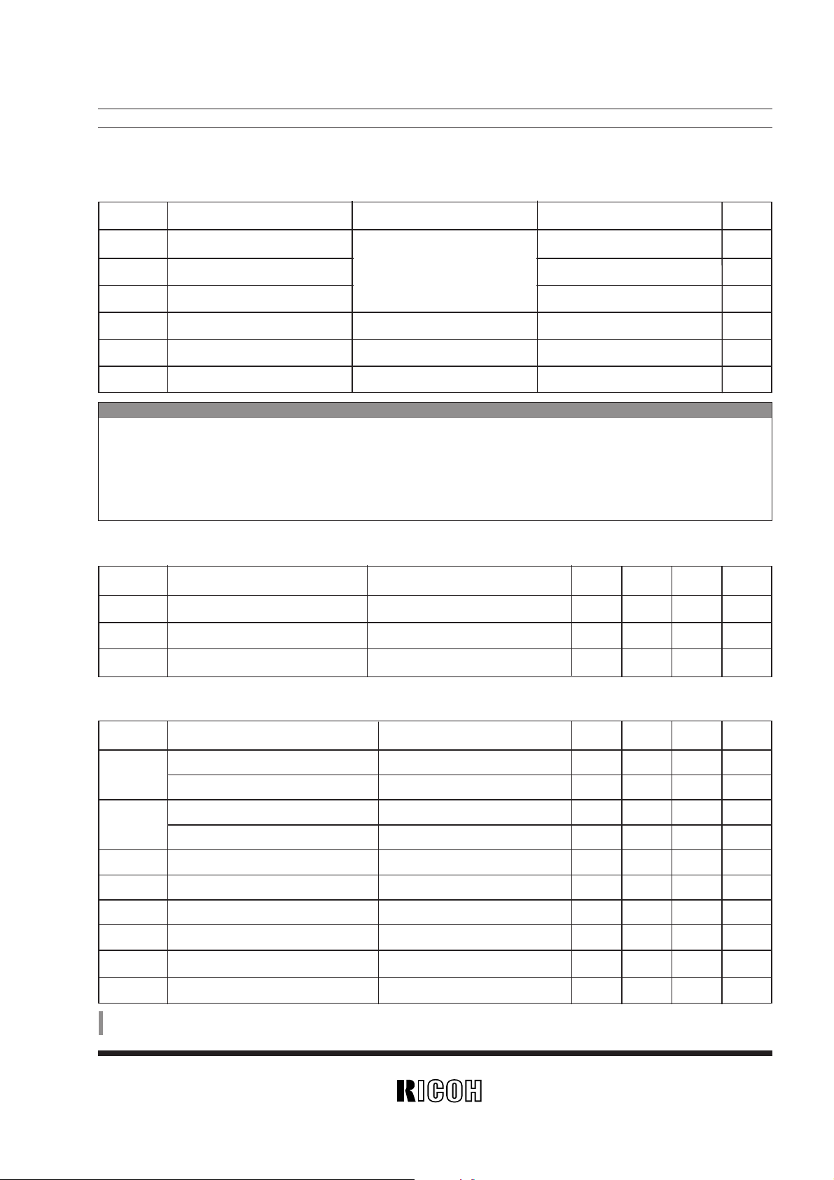
ABSOLUTE MAXIMUM RATINGS
RECOMMENDED OPERATING CONDITIONS
Symbol Item Conditions Ratings Unit
VCC Supply Voltage –0.3 to 7.0 V
VI Input Voltage –0.3 to VCC+0.3 V
VO Output Voltage –0.3 to VCC+0.3 V
Pd Maximum Power Dissipation Ta=25˚C 700 mW
Topr Operating Temperature 0 to 70 ˚C
Tstg Storage Temperature –40 to 125 ˚C
Symbol Item Conditions MIN. TYP. MAX. Unit
VCC Supply Voltage 4.75 5 5.25 V
VDH Data Preservation Voltage 2.2 5.25 V
fXT Crystal Oscillation Frequency 32.768 kHz
Referenced at GND pin
(Unless otherwise specified, Ta=0 to 70˚C)
DC ELECTRICAL CHARACTERISTICS
Symbol Item Conditions MIN. TYP. MAX. Unit
VIH
“H” Input Voltage (excluding OSCIN) 2.0
Vcc
V
“H” Input Voltage (OSCIN) 4.0
Vcc
V
VIL
“L” Input Voltage (excluding OSCIN) –0.3 0.8 V
“L” Input Voltage (OSCIN) –0.3 0.5 V
VOH “H” Output Voltage IOH=–400µA 2.4 V
VOL “L” Output Voltage IOL=2mA 0.4 V
II Input Voltage VI=0 to 5.25V ±10 µA
IOZ Output Off-state Leakage Current ±10 µA
ICC1 Supply Current for backup fXT=32.768kHz, Vcc=2.2V 15 µA
I
CC2 Operating Supply Current fXT=32.768kHz, Vcc=5.0V*
2
250 µA
(Unless otherwise specified, Ta=0 to 70˚C, Vcc=5V±10%)
*
1) Plus (without sign) direction of current is assumed to be the direction flowing into IC.
*
2) When connected to CPU (Read/Write cycle 10µs)
ABSOLUTE MAXIMUM RATINGS
Absolute Maximum ratings are threshold limit values that must not be exceeded even for an instant under
any conditions. Moreover, such values for any two items must not be reached simultaneously. Operation
above these absolute maximum ratings may cause degradation or permanent damage to the device. These
are stress ratings only and do not necessarily imply functional operation below these limits.
 Loading...