

Page 1

RICOH COMPANY,LTD.
R5C841
PCI-CardBus/IEEE1394/SD Card
/MemoryStick/xD/ExpressCard
Data Sheet
REV. 1.10
12345
Page 2
–REVISION HISTORY–
REVISION DATE COMMENTS
0.60 7/24/03 First Draft (described Overview, Block Diagram and Pin description only)
0.70 9/10/03 Addition of the regulator description (Spec 4) and the electrical characteristics
(Spec 5).
0.80 11/6/03 Change from NewCard to ExpressCard.
Mistakes in writing are corrected.
1.00 1/30/04 First Public Release
Mistakes in writing are corrected.
1.10 5/18/04 Changes in the chart of Global Reset Timing (Ch. 5.3.6).
Deletion of the 2.5V power supply support for the core logic.
RICOH COMPANY,LTD.
12345 2004 REV. 1.10
Page 3

R5C841 PCI-CardBus/IEEE 1394/SD Card/Memory Stick/xD/ExpressCard Data Sheet
1 OVERVIEW
The R5C841 is a single chip solution offering five PCI functions (a PCI bus bridge to a PC Card, an IEEE
1394, an SD Card, a Memory Stick and an xD Picture Card) with an ExpressCard (USB Interface Type)
switch.
PC98/99/2001 compliant
PC2001 Design Guide compliant (Subsystem ID, Subsystem Vendor ID)
Compliant with ACPI and PCI Bus Power Management 1.1
Support Global Reset
Low Power consumption
Low operating power consumption due to the improvement of Power Management
Software Suspend mode compliant with ACPI
Hardware Suspend
CLKRUN#, CCLKRUN# support
The core logic - powered at 1.8V, the others – powered at 3.3V
PCI-CardBus/1394 Bridge/SD Card/Memory Stick/xD Picture Card/ExpressCard interface
1-slot PC Card
2 ports of IEEE1394
MDIOxx pins shared by SD Card, Memory Stick and xD Picture Card
− Providing Ricoh’s proprietary driver for Memory Stick and xD Picture Card
ExpressCard (USB Interface Type) supported by the PC Card passive adapter
PCI Bus Interface
Compliant with PCI Local Bus Specification2.3
The maximum frequency 33MHz
PCI Master/Target protocol support
PCI configuration space for each function
3.3V Interface (5V tolerant)
CardBus PC card Bridge
Compliant with PC Card Standard Release 8.1 Specification
The maximum frequency 33MHz
Support CardBus Master/Target protocol
Support Memory Write Posting/ Read Prefetching
Transfer transactions
− All memory read/write transaction (bi-direction)
− I/O read/write transaction (bi-direction)
− Configuration read/write transaction (PCI → Card)
− 2 programmable memory windows
− 2 programmable I/O windows
PC Card-16 Bridge
Compliant with PC Card Standard Release 8.1 16-bit Specification
5 programmable memory windows
2 programmable I/O windows
Compliant with i82365SL compatible register set/ExCA
Support Legacy 16-bit mode (3E0, 3E2 I/O ports)
12345 2004 REV. 1.10 1-1
Page 4

R5C841 PCI-CardBus/IEEE 1394/SD Card/Memory Stick/xD/ExpressCard Data Sheet
IEEE1394 Interface
Compliant with IEEE1394-1995 Standard Specification and IEEE1394a-2000 Standard Specification
Compliant with 1394 OHCI Release 1.1/1.0 Standard Specification
Support Cycle Master
Provide the Asynchronous receive/transmit FIFO and isochronous receive/transmit FIFO
Support Self-ID, physical DMA
Data transmission rate of 100, 200 and 400Mbps
2 ports of 1394 Cable interface
24.576MHz crystal oscillator and Internal 393.216MHz PLL
Support Cable Power monitoring (CPS)
Set Initial values of Power Class and CMC by PCI Configuration registers
Small Card Interface
SD Card
− Compliant with SD Memory Card Specification Version 1.01
− Compliant with SD Input/Output (SDIO) Card Specification Version 1.0
− Compliant with SD Host Controller Standard Specification Version 1.0
Memory Stick
− Compliant with Memory Stick Standard Format Specification Version 1.4
− Compliant with Memory Stick PRO Format Specification Version 1.00
• xD Picture Card
− Compliant with xD Picture Card Specification Version 1.00
− Compliant with xD Picture Card Host Guideline Version 1.00
− Backward compatible with the Smart Media
ExpressCard Interface
Compliant with EXPRESSCARD STANDARD Draft Release 1.0
Pass USB signals from a USB-HOST to a Card Slot
System Interrupt
Support INTA#, INTB# and INTC# for PC system interrupt (Each unit is programmable.)
Support Serialized IRQ
IRQx support for ISA system interrupt
Support Remote Wake Up by CSTSCHG
Support an internal regulator to convert the 3.3V power into the power for the internal core logic
Support Zoomed Video Port (Bypass type)
Support PC Card LED, 1394 LED, SD LED, Memory Stick LED and xD Picture Card LED
Support BAY function with the PC Card passive adapter
Pin Compatible With: R5C811 (CSP1616-208)
R5C821 (CSP1616-208)
R5C821PA (CSP1616-208)
R5C851 (CSP1616-208)
R5C851PA (CSP1616-208)
Package
208pin CSP (size=16x16mm, pitch=0.8mm, t=1.4mm)
(USB Interface Type only)
12345 2004 REV. 1.10 1-2
Page 5
R5C841 PCI-CardBus/IEEE 1394/SD Card/Memory Stick/xD/ExpressCard Data Sheet
A
r
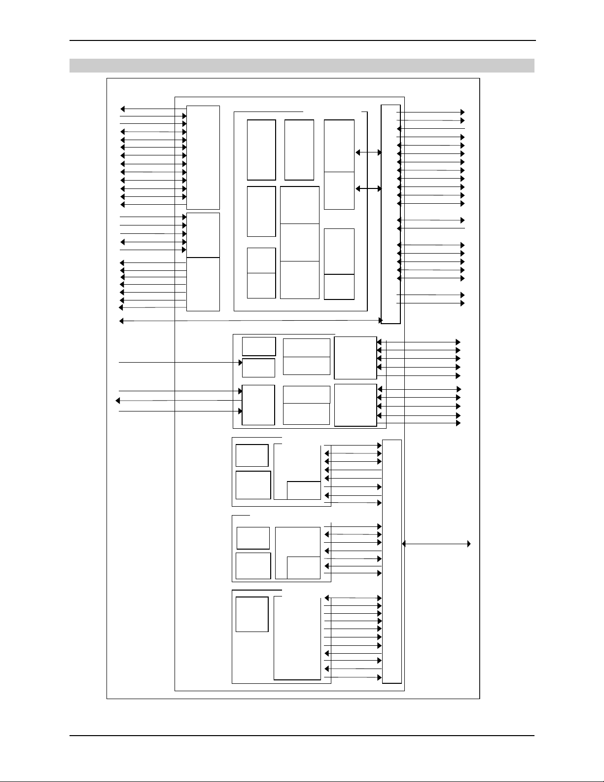
2 BLOCK DIAGRAM
R5C841 Block Diagram
REQ#
GNT#
IDSEL
AD[31:0]
PAR
FRAME#
IRDY#
TRDY#
STOP#
PERR#
SERR#
PCICLK
PCIRST#
GBRST#
INTA#
INTB#
INTC#
SPKROUT
CPS
XI
XO
FIL0
C/BE[3:0]#
DEVSEL#
CLKRUN#
HWSPND#
SRIRQ#/UDIO0
UDIO1-UDIO5
RI_OUT#/PME#
USBDP, USBDM
Socket (Func#0)
CardBus
Interface
Master &
Target
16-bit
Interface
Master
Socket
Status &
Control
A
Socket
Power
Control
M
U
X
&
CardBus
Address
Decode
&
Mapping
ADDR/DATA
Buffer
PCI to Card
Buffer
Manage
ADDR/DAT
Buffer
Card to PCI
PCI
Interface
RESET
&
Clock
Interrupt
&
Audio
PCI
Address
Decode
Mapping
PCI
Config.
Registers
CardBus
Registers
16-bit
Registers
1394 I/F (Func#1)
1394
Registers
PHY
Registers
PLL
OHCI
Controller
LINK Core
LINK
Interface
rbitration
& Control
Cable Port 0
Cable Port 1
CCLK
CRST#
CREQ#
CGNT#
CCLKRUN#
CAD[31:0]
CC/BE[3:0]#
CPAR
CFRAME#
CDEVSEL#
CIRDY#
CTRDY#
CPERR#
CSERR#
CCD1,2#
CVS1,2
CSTSCHG
CINT#
CAUDIO
VCC3EN#, VCC5EN#
VPPEN0, VPPEN1
TPAP0
TPAN0
TPBP0
TPBN0
TPBIAS0
TPAP1
TPAN1
TPBP1
TPBN1
TPBIAS1
SD I/F (Func#2)
SD
Registers
Clock
Control
MS
Registers
Clock
Control
Registers
SD Card
Interface
Memory Stick I/F (Func#3)
Memory Stick
xD I/F (Func #4)
xD Pictu re Car d xD
Interface
Buffer
RAM
Interface
Buffe
RAM
SDCCLK
SDCDAT[3:0]
SDCCMD
SDCD#
SDWP#
SDPWR[1:0]
SDEXTCK
SDLED#
MSCCLK
MSCDAT [3:0]
MSBS
MSCD#
MSPWR
MSEXTCK
MSLED#
XDCDAT[7:0]
XDALE
XDCLE
XDCE#
XDW E#
XDRE#
XDPW R
XDCD[1:0]#
XDLED#
XDR/B#
XDW P#
M
U
X
MDIO [19:00]
12345 2004 REV.1.10 2-1
Page 6

R5C841 PCI-CardBus/IEEE 1394/SD Card/Memory Stick/xD/ExpressCard Data Sheet
N
T
_
A
A
A
A
A
A
A
A
A
A
A
_
A
A
A
A
A
_
A
A
A
A
A
AD7AD6A
A
_
A
AD4A
_
A
AD1A
_
T
A
A
_
A
A
V
A
A
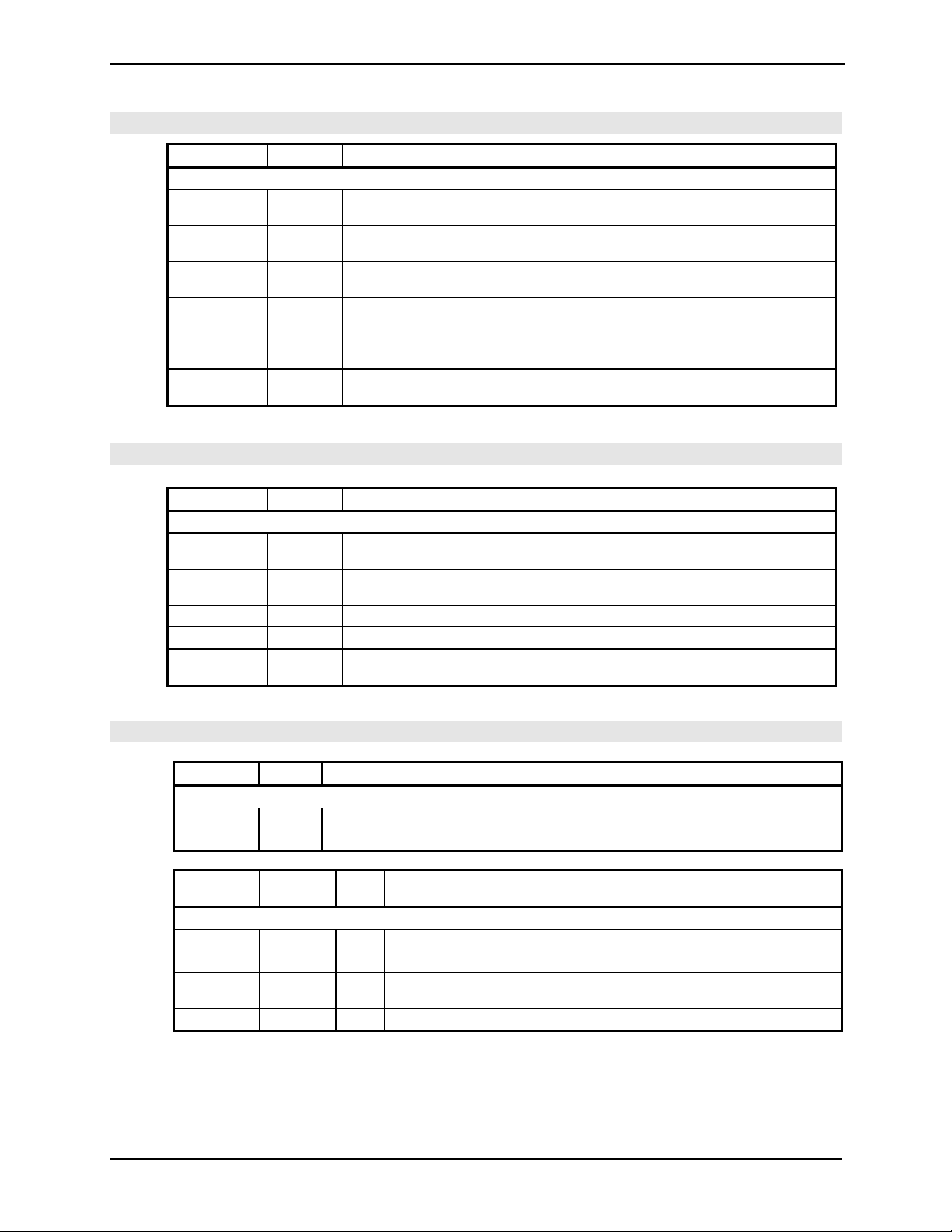
3 PIN DESCRIPTION
3.1 Pin Assignments (208 pin CSP)
CSP Pin Assignment
Bottom View
A B C D E F G H J K L M
1
³ { { { { { { { z{ { { { { { { {
2
{
MDIO01
3
{ {
MDIO02 MDIO 03
4
{
VCC
MD3V
5
{ {
MDIO05 MDIO 06 MDIO07
6
{ {
MDIO08 MDIO09 MDIO10 MDIO11
7
{ {
MDIO12 MDIO 13 MDIO14 MDI O15
8
{ {
MDIO16 MDIO17 MDIO18 MDI O19
9
z
GND AGND
10
{ {
TPAN1 TPAP1 TPBIAS1
11
{ {
12
{ {
13
{ {
14
{ {
15
z z
GND AGND
16
{ {
XI XO
17
VCC_
PHY3V
18
19
{
WP/
IOIS16#
NC
MDIO00 NC
{ { { { { { { { { { { { { { {
NC
NC
NC
NC
SPKROUT
HWSPND#
UDIO5
GBRST#
UDIO1
UDIO2
GND
INTA#
PCICLK
INTC#
MDIO04
z
VCC_
PHY3V
{ { { { { { { { { { { { { { {
CDATA9 CDATA8 BVD1 CADR1 CADR3 CADR5 CADR25 CADR12 CADR21
{ { { { { { { {z { { { { { {
CDATA2 CDATA10 CDATA1 CDATA0 BVD2 INPACK# RESET VCC_3
{ { { { { { { { { { {
NC
{
{ {
{ {
{ {
z z
GND GND
{
{
{ {
{
z
GND
{
CD2#
VCC_
PHY3V
VCC_
PHY3V
VCC
RIN
VCC_
ROUT
{ { { { { { { { { { {
CADR0 REG# WAIT# VS2# CADR7 CADR23 CADR22 CADR20 CADR18 CADR17 VS1#
RI_OUT#/
TES
PME#
{ z z { { { {
VCC_3V
VCC_3V
UDIO3
UDIO4
UDIO0/
SRIRQ #
GND
INTB#
GND
{ { { { { z { { {
CADR2 CADR4 CADR6 CADR24 CADR15
VCC_3V CADR16 GND CADR19 IOWR# CADR9 OE# CADR10 CE1#
VCC
ROUT
NC
PCIRST#
CLKRUN#
GND
D30
D31
REQ#
GNT#
WE# CADR13 CADR8
RDY/
CADR14 IORD# CARD11 CE2# CDATA15
IREQ#
P R T U V W
D26
D27
D28
D29
C/BE3#
IDSEL
D24
D25
REGEN#
PCI3V
VCC
PCI3V
VCC5EN# VCC3EN# VPPEN0 VPPEN1TPBN0 TPBP0 VREF
CDATA3 CD1# USBDP USBDMFIL0 REX
D21
D19
D22
D20
D23
{
DEVSE L#
{
VCC
RIN
{
{ {
D12 AD11
{ {
z z
GND
{
VCC
{
{ {
{ {
SERR# PAR C/BE1#
{
D15
D8 C/BE0#
GND GND
GND
D5
D2
{
CDATA4 CDATA11 CDATA5
D17
D18
FRAME#
CDATA12 CDATA6
CDATA13 CDATA7
D16
{
C/BE2#
{
VCC
PCI3V
{ {
IRDY# TRDY#
{ {
STOP# PERR#
{ {
{ {
D14AD13
{ {
D10AD9
{ {
z z
{ {
D3TPBN1 TPBP1 CPS
{ {
D0TPAN0 TPAP0 TPBIAS0 NC
{ {
{ {
{ {
{ {
{ {
{
CDATA14
12345 2004 REV. 1.10 3-1
Page 7
R5C841 PCI-CardBus/IEEE 1394/SD Card/Memory Stick/xD/ExpressCard Data Sheet
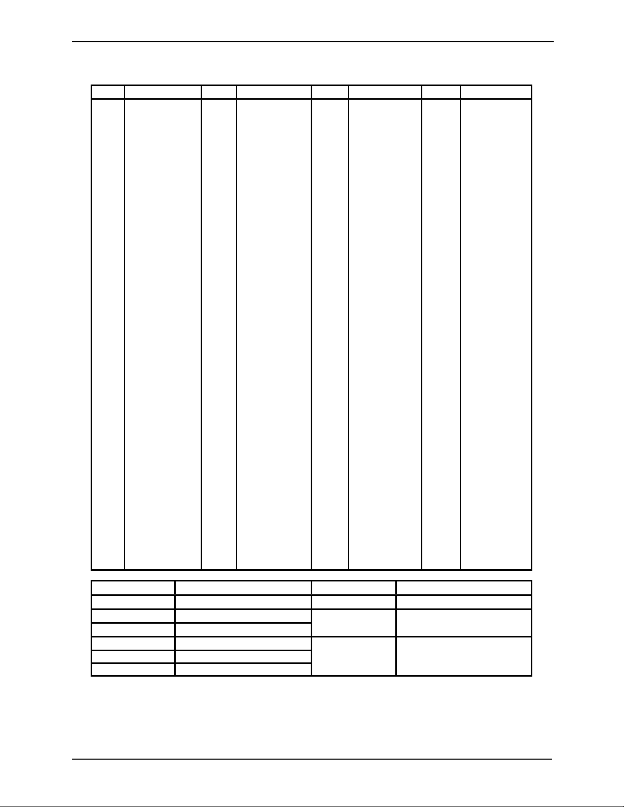
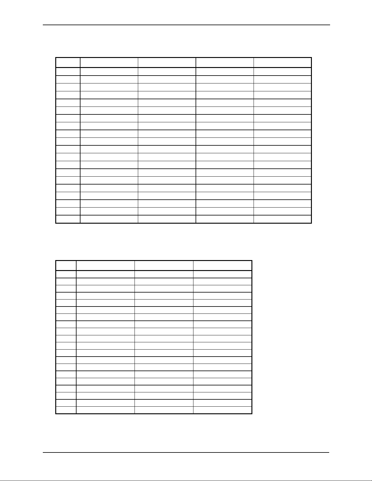
• CSP Pin List
Ball Signal Name Ball Signal Name Ball Signal Name Ball Signal Name
F4 TEST V5 STOP# T19 OE# C19 CDATA2
F2 HWSPND# W5 PERR# R16 VS1# B19 CDATA10
F1 SPKROUT T6 SERR# R18 CADR11 A18 WP/IOIS16#
G4 RI_OUT#/PME# V6 PAR R19 CADR9 D15 CD2#
G2 GBRST# W6 C/BE1# P18 IORD# E8 MDIO19
G1 UDIO5 T7 AD15 P19 IOWR# D8 MDIO18
H5 UDIO4 V7 AD14 P15 CADR8 B8 MDIO17
H4 UDIO3 W7 AD13 P16 CADR17 A8 MDIO16
H2 UDIO2 R8 AD12 N15 CADR13 E7 MDIO15
H1 UDIO1 T8 AD11 N16 CADR18 D7 MDIO14
J4 UDIO0/SRIRQ# V8 AD10 N18 CADR14 B7 MDIO13
J2 INTA# W8 AD9 N19 CADR19 A7 MDIO12
K4 INTB# R9 AD8 M15 WE# E6 MDIO11
K2 INTC# T9 C/BE0# M16 CADR20 D6 MDIO10
L5 CLKRUN# V9 AD7 M18 RDY/IREQ# B6 MDIO09
L4 PCIRST# W9 AD6 L16 CADR22 A6 MDIO08
K1 PCICLK T11 AD5 L18 CADR21 D5 MDIO07
M5 GNT# V11 AD4 L19 CADR16 B5 MDIO06
M4 REQ# W11 AD3 K15 CADR15 A5 MDIO05
M2 AD31 T12 AD2 K16 CADR23 B4 MDIO04
M1 AD30 V12 AD1 K18 CADR12 B3 MDIO03
N5 AD29 W12 AD0 J15 CADR24 A3 MDIO02
N4 AD28 R13 VCC5EN# J16 CADR7 A2 MDIO01
N2 AD27 T13 VCC3EN# J18 CADR25 B1 MDIO00
N1 AD26 V13 VPPEN0 H15 CADR6 B16
P5 AD25 W13 VPPEN1 H16 VS2# A16
P4 AD24 V14 USBDP H18 CADR5 B14
P2 C/BE3# W14 USBDM H19 RESET A14
P1 IDSEL R14 CDATA3 G15 CADR4 D13
R4 AD23 T14 CD1# G16 WAIT# B13
R2 AD22 T15 CDATA4 G18 CADR3 A13
R1 AD21 V15 CDATA11 G19 INPACK# D12
T2 AD20 W15 CDATA5 F15 CADR2 B12
T1 AD19 V16 CDATA12 F16 REG# A12
U2 AD18 W16 CDATA6 F18 CADR1 D11
U1 AD17 V17 CDATA13 F19 BVD2 B11
V1 AD16 W17 CDATA7 E16 CADR0 A11
W2 C/BE2# W18 CDATA14 E18 BVD1 D10
V3 FRAME# V19 CE1# E19 CDATA0 B10
V4 IRDY# U18 CDATA15 D18 CDATA8 A10
W4 TRDY# U19 CADR10 D19 CDATA1 R7 REGEN#
T5 DEVSEL# T18 CE2# C18 CDATA9
XO
XI
REXT
FIL0
VREF
TPBP0
TPBN0
TPBIAS0
TPAP0
TPAN0
CPS
TPBP1
TPBN1
TPBIAS1
TPAP1
TPAN1
Pin Name Ball# Pin Name Ball#
VCC_PCI3V W3, R11, R12
VCC_3V F5, G5, J19, K19
VCC_MD3V A4
VCC_RIN R6, E13
VCC_ROUT L1, E14
AVCC_PHY3V E10, E11, A17, B17
AGND A9, B9, D9, D14, A15, B15
GND
NC L2, C1, D1, E1, C2, D2, E2,
J1, J5, K5, E9, R10, T10, V10,
W10, L15, M19
E4, E12
12345 2004 REV. 1.10 3-2
Page 8
R5C841 PCI-CardBus/IEEE 1394/SD Card/Memory Stick/xD/ExpressCard Data Sheet
3.2 Pin Characteristics
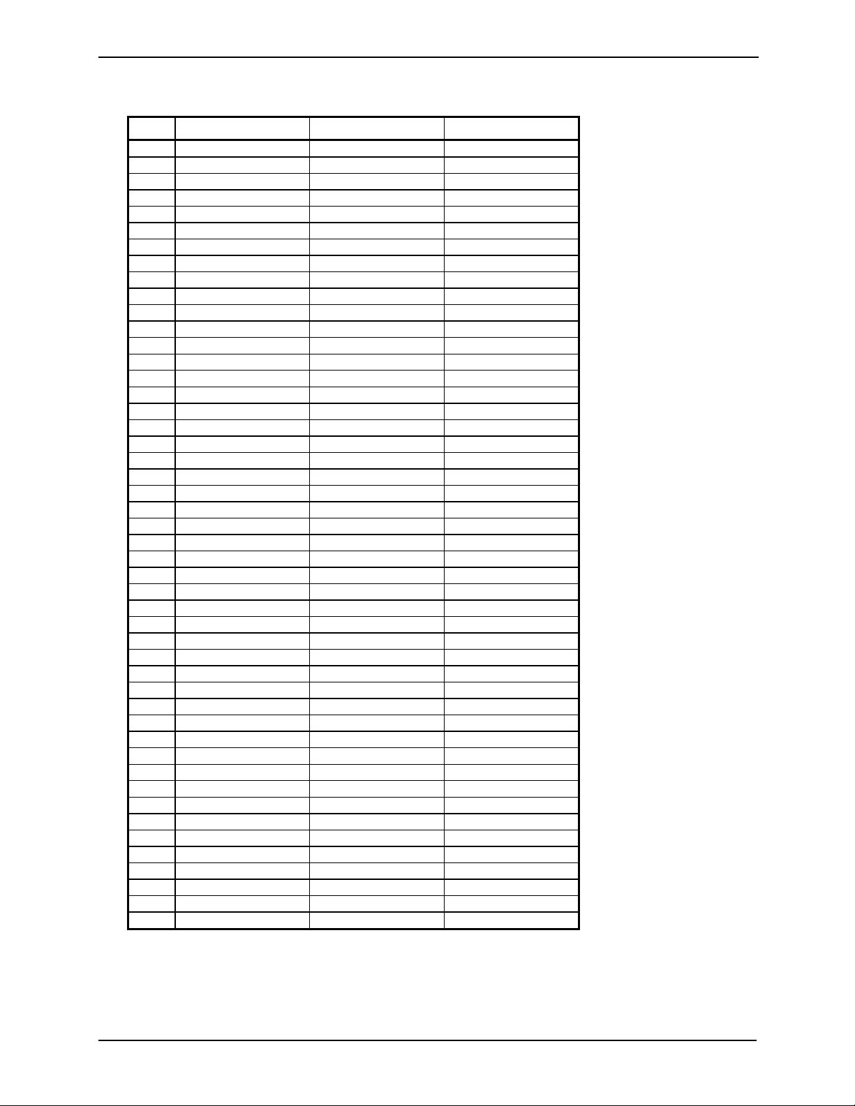
16-bit Card Interface CardBus Card Interface Pin Characteristics
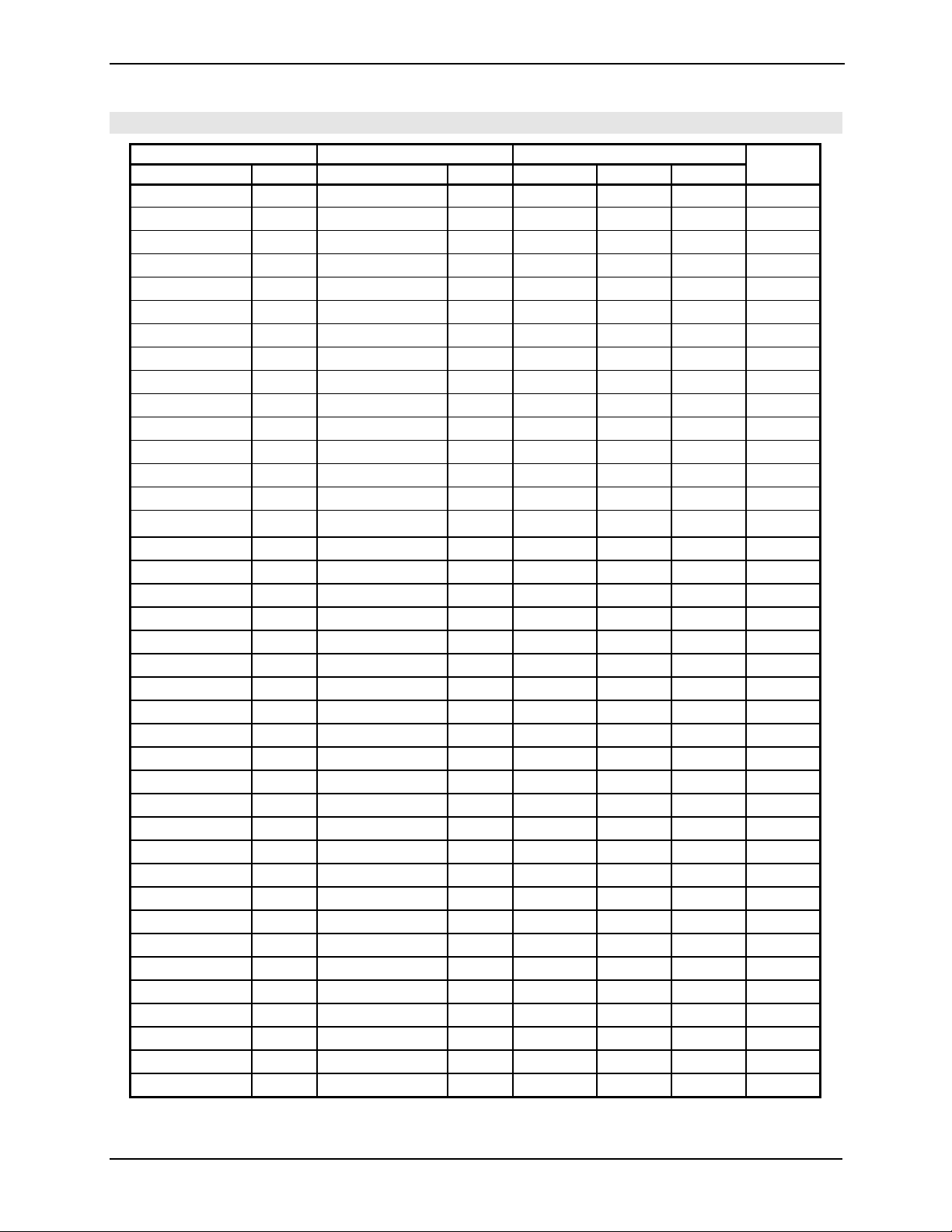
Pin Name Dir Pin Name Dir 5Vtolerant PwrRail Drive
TEST I TEST I 3V –
HWSPND# I HWSPND# I 3V –
SPKROUT I/O SPKROUT I/O 3V 4mA
RI_OUT#/ PME# O (OD) RI_OUT#/ PME# O (OD) 3V 4mA
GBRST# I GBRST# I 3V –
UDIO5 O UDIO5 O 3V 4mA
UDIO4 I/O UDIO4 I/O 3V 4mA
UDIO3 I/O UDIO3 I/O 3V 4mA
UDIO2 I/O UDIO2 I/O 3V 4mA
UDIO1 I/O UDIO1 I/O 3V 4mA
UDIO0/ SRIRQ# I/O UDIO0/ SRIRQ# I/O 3V 4mA
INTA# O (OD) INTA# O (OD) P PCI
INTB# O (OD) INTB# O (OD) P PCI
INTC# O (OD) INTC# O (OD) P PCI
CLKRUN# I/O CLKRUN# I/O P PCI
PCIRST# I PCIRST# I P –
PCICLK I PCICLK I P –
GNT# I GNT# I P –
REQ# O (TS) REQ# O (TS) P PCI
AD31 I/O AD31 I/O P PCI
AD30 I/O AD30 I/O P PCI
AD29 I/O AD29 I/O P PCI
AD28 I/O AD28 I/O P PCI
AD27 I/O AD27 I/O P PCI
AD26 I/O AD26 I/O P PCI
AD25 I/O AD25 I/O P PCI
AD24 I/O AD24 I/O P PCI
C/BE3# I/O C/BE3# I/O P PCI
IDSEL I IDSEL I P –
AD23 I/O AD23 I/O P PCI
AD22 I/O AD22 I/O P PCI
AD21 I/O AD21 I/O P PCI
AD20 I/O AD20 I/O P PCI
AD19 I/O AD19 I/O P PCI
AD18 I/O AD18 I/O P PCI
AD17 I/O AD17 I/O P PCI
AD16 I/O AD16 I/O P PCI
C/BE2# I/O C/BE2# I/O P PCI
FRAME# I/O FRAME# I/O P PCI
Note
12345 2004 REV. 1.10 3-3
Page 9
R5C841 PCI-CardBus/IEEE 1394/SD Card/Memory Stick/xD/ExpressCard Data Sheet
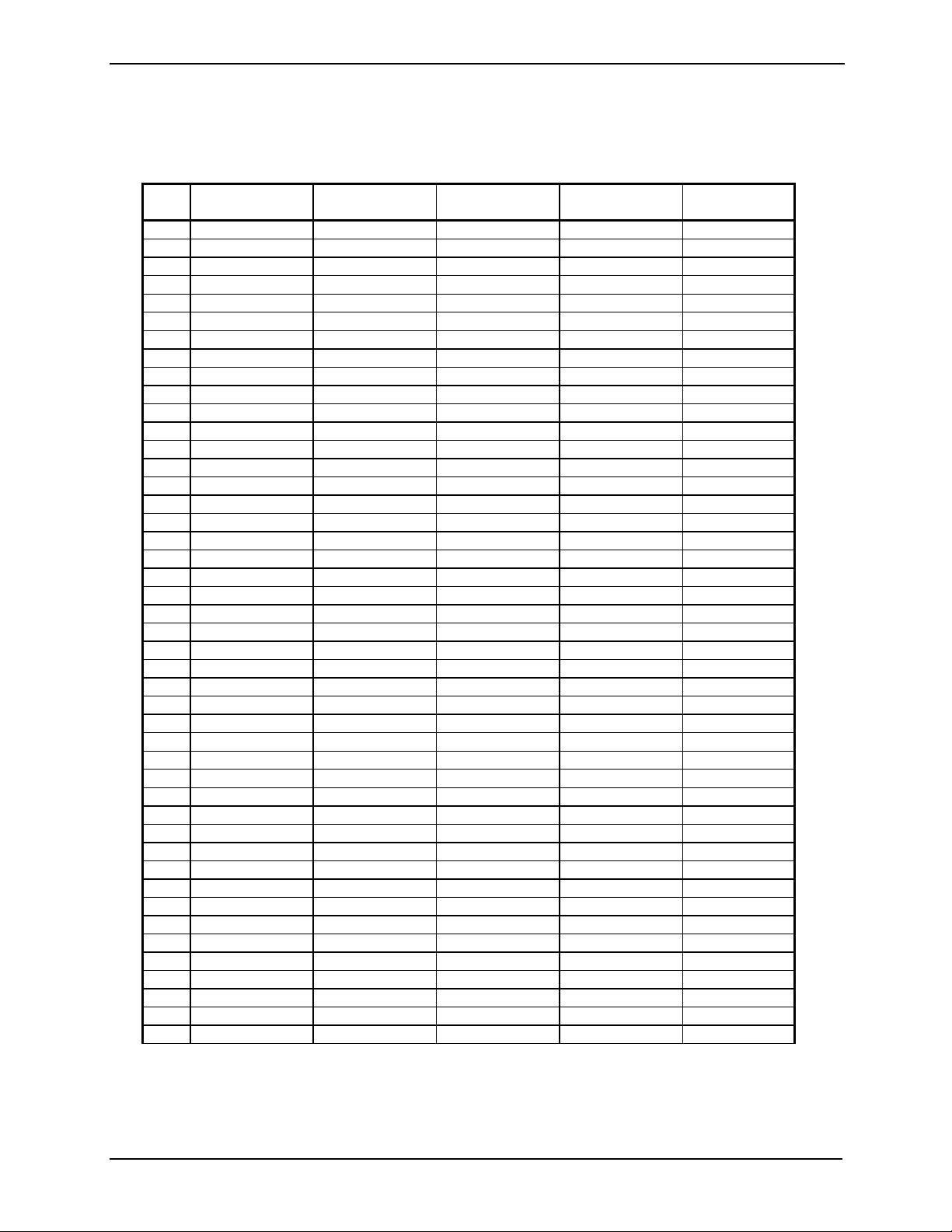
16-bit Card Interface CardBus Card Interface Pin Characteristics
Pin Name Dir Pin Name Dir 5Vtolerant PwrRail Drive
IRDY# I/O IRDY# I/O P PCI
TRDY# I/O TRDY# I/O P PCI
DEVSEL# I/O DEVSEL# I/O P PCI
STOP# I/O STOP# I/O P PCI
PERR# I/O PERR# I/O P PCI
SERR# O (OD) SERR# O (OD) P PCI
PAR I/O PAR I/O P PCI
C/BE1# I/O C/BE1# I/O P PCI
AD15 I/O AD15 I/O P PCI
AD14 I/O AD14 I/O P PCI
AD13 I/O AD13 I/O P PCI
AD12 I/O AD12 I/O P PCI
AD11 I/O AD11 I/O P PCI
AD10 I/O AD10 I/O P PCI
AD9 I/O AD9 I/O P PCI
AD8 I/O AD8 I/O P PCI
C/BE0# I/O C/BE0# I/O P PCI
AD7 I/O AD7 I/O P PCI
AD6 I/O AD6 I/O P PCI
AD5 I/O AD5 I/O P PCI
AD4 I/O AD4 I/O P PCI
AD3 I/O AD3 I/O P PCI
AD2 I/O AD2 I/O P PCI
AD1 I/O AD1 I/O P PCI
AD0 I/O AD0 I/O P PCI
VCC5EN# O VCC5EN# O 3V 4mA
VCC3EN# O VCC3EN# O 3V 4mA
VPPEN0 O VPPEN0 O 3V 4mA
VPPEN1 O VPPEN1 O 3V 4mA
USBDP I/O USBDP I/O – –
USBDM I/O USBDM I/O – –
CDATA3 I/O CAD0 I/O 3V 4mA
CD1# I (PU) CCD1# I (PU) 3V –
CDATA4 I/O CAD1 I/O 3V 4mA
CDATA11 I/O CAD2 I/O 3V 4mA
CDATA5 I/O CAD3 I/O 3V 4mA
CDATA12 I/O CAD4 I/O 3V 4mA
CDATA6 I/O CAD5 I/O 3V 4mA
CDATA13 I/O CAD6 I/O 3V 4mA
CDATA7 I/O CAD7 I/O 3V 4mA
CDATA14 I/O – – 3V 4mA
Note
12345 2004 REV. 1.10 3-4
Page 10
R5C841 PCI-CardBus/IEEE 1394/SD Card/Memory Stick/xD/ExpressCard Data Sheet
16-bit Card Interface CardBus Card Interface Pin Characteristics
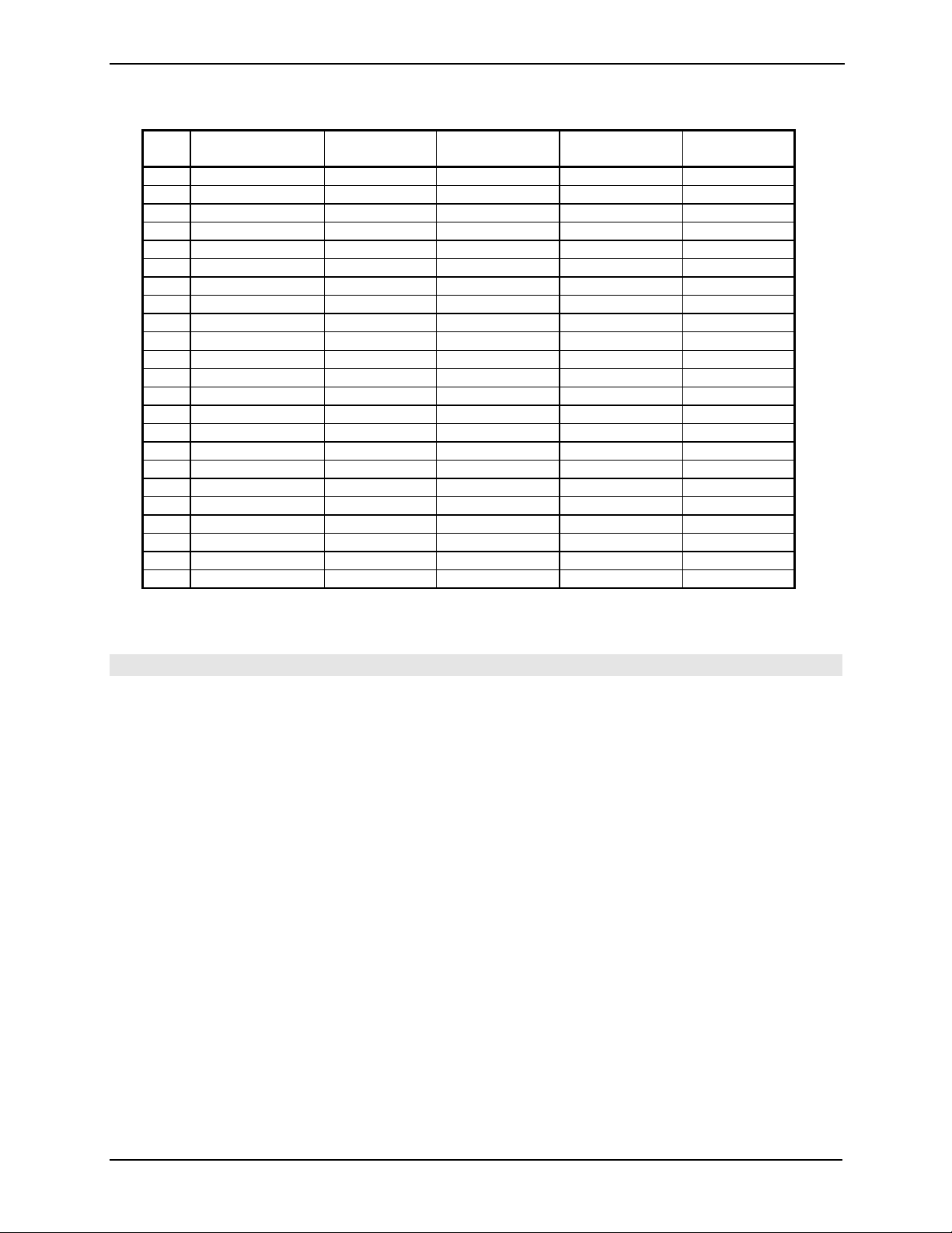
Pin Name Dir Pin Name Dir 5Vtolerant PwrRail Drive
CE1# O CC/BE0# I/O 3V 4mA
CDATA15 I/O CAD8 I/O 3V 4mA
CADR10 O CAD9 I/O 3V 4mA
CE2# O CAD10 I/O 3V 4mA
OE# O CAD11 I/O 3V 4mA
VS1# I/O CVS1 I/O 3V 1mA
CADR11 O CAD12 I/O 3V 4mA
IORD# O CAD13 I/O 3V 4mA
CADR9 O CAD14 I/O 3V 4mA
IOWR# O CAD15 I/O 3V 4mA
CADR8 O CC/BE1# I/O 3V 4mA
CADR17 O CAD16 I/O 3V 4mA
CADR13 O CPAR I/O 3V 4mA
CADR18 O – – 3V 4mA
CADR14 O CPERR# I/O (PU) 3V 4mA 1
CADR19 O – I/O (PU) 3V 4mA 1
WE# O CGNT# O 3V 4mA
CADR20 O CSTOP# I/O (PU) 3V 4mA 1
RDY/ IREQ# I (PU) CINT# I (PU) 3V –
CADR21 O CDEVSEL# I/O (PU) 3V 4mA 1
CADR16 O (TS) CCLK O (TS) 3V CB
CADR22 O CTRDY# I/O (PU) 3V 4mA 1
CADR15 O CIRDY# I/O (PU) 3V 4mA 1
CADR23 O CFRAME# I/O 3V 4mA
CADR12 O CC/BE2# I/O 3V 4mA
CADR24 O CAD17 I/O 3V 4mA
CADR7 O CAD18 I/O 3V 4mA
CADR25 O CAD19 I/O 3V 4mA
CADR6 O CAD20 I/O 3V 4mA
VS2# I/O CVS2 I/O 3V 1mA
CADR5 O CAD21 I/O 3V 4mA
RESET O (TS) CRST# O (TS) 3V 2mA
CADR4 O CAD22 I/O 3V 4mA
WAIT# I (PU) CSERR# I (PU) 3V –
CADR3 O CAD23 I/O 3V 4mA
INPACK# I (PU) CREQ# I (PU) 3V –
CADR2 O CAD24 I/O 3V 4mA
REG# O CC/BE3# I/O 3V 4mA
CADR1 O CAD25 I/O 3V 4mA
BVD2/
SPKR#/
LED
I (PU) CAUDIO I (PU) 3V –
Note
12345 2004 REV. 1.10 3-5
Page 11
R5C841 PCI-CardBus/IEEE 1394/SD Card/Memory Stick/xD/ExpressCard Data Sheet
16-bit Card Interface CardBus Card Interface Pin Characteristics
Pin Name Dir Pin Name Dir 5Vtolerant PwrRail Drive
CADR0 O CAD26 I/O 3V 4mA
BVD1/
STSCHG#/
RI#
CDATA0 I/O CAD27 I/O 3V 4mA
CDATA8 I/O CAD28 I/O 3V 4mA
CDATA1 I/O CAD29 I/O 3V 4mA
CDATA9 I/O CAD30 I/O 3V 4mA
CDATA2 I/O – – 3V 4mA
CDATA10 I/O CAD31 I/O 3V 4mA
WP/ IOIS16# I (PU) CCLKRUN# I/O (PU) 3V 4mA 1
CD2# I (PU) CCD2# I (PU) 3V –
MDIO00 I (PU) MDIO00 I (PU) 3V
MDIO01 I (PU) MDIO01 I (PU) 3V
MDIO02 O (PU) MDIO02 O (PU) 3V 8mA
MDIO03 I (PU) MDIO03 I (PU) 3V
MDIO04 O MDIO04 O 3V 8mA
MDIO05 (SD)
(MS)
(xD)
MDIO06 O MDIO06 O 3V 8mA
MDIO07 I MDIO07 I 3V
MDIO08 (SD)
(MS)
(xD)
MDIO09 (SD)
(MS)
(xD)
MDIO10 (SD)
(MS)
(xD)
MDIO11 (SD)
(MS)
(xD)
MDIO12 (SD)
(MS)
(xD)
MDIO13 (SD)
(MS)
(xD)
MDIO14 I/O(PD) MDIO14 I/O(PD) M 8mA
MDIO15 I/O(PD) MDIO15 I/O(PD) M 8mA
MDIO16 I/O(PD) MDIO16 I/O(PD) M 8mA
MDIO17 I/O(PD) MDIO17 I/O(PD) M 8mA
MDIO18 O(PD) MDIO18 O(PD) M 8mA
MDIO19 O(PD) MDIO19 O(PD) M 8mA
I (PU) CSTSCHG I (PD) 3V – 2
—
—
—
O/
—/
O(PD)
I/O(PU)/
O(TS)/
O(PU)
I/O(PU)/
I/O(PU)/
O(PU)
I/O(PU)/
I/O/
I/O(PD)
I/O(PU)/
I/O/
I/O(PD)
I/O(PU)/
I/O/
I/O(PD)
I/O(PU)/
I/O/
I/O(PD)
MDIO05 (SD)
(MS)
(xD)
MDIO08 (SD)
(MS)
(xD)
MDIO09 (SD)
(MS)
(xD)
MDIO10 (SD)
(MS)
(xD)
MDIO11 (SD)
(MS)
(xD)
MDIO12 (SD)
(MS)
(xD)
MDIO13 (SD)
(MS)
(xD)
O/
—/
O(PD)
I/O(PU)/
O(TS)/
O(PU)
I/O(PU)/
I/O(PU)/
O(PU)
I/O(PU)/
I/O/
I/O(PD)
I/O(PU)/
I/O/
I/O(PD)
I/O(PU)/
I/O/
I/O(PD)
I/O(PU)/
I/O/
I/O(PD)
3V 8mA
—
M 8mA
M 8mA
M 8mA
M 8mA
M 8mA
M 8mA
Note
12345 2004 REV. 1.10 3-6
Page 12
R5C841 PCI-CardBus/IEEE 1394/SD Card/Memory Stick/xD/ExpressCard Data Sheet
16-bit Card Interface CardBus Card Interface Pin Characteristics
Pin Name Dir Pin Name Dir 5Vtolerant PwrRail Drive
XI I XI I AP
XO O XO O AP
FIL0 I/O FIL0 I/O AP
CPS I(PD) CPS I(PD) AP 1394
VREF I/O VREF I/O AP
REXT I/O REXT I/O AP
TPBN0 I/O TPBN0 I/O AP 1394
TPBP0 I/O TPBP0 I/O AP 1394
TPAN0 I/O TPAN0 I/O AP 1394
TPAP0
TPBIAS0
TPBN1 I/O TPBN1 I/O AP 1394
TPBP1 I/O TPBP1 I/O AP 1394
TPAN1 I/O TPAN1 I/O AP 1394
TPAP1 I/O TPAP1 I/O AP 1394
TPBIAS1 I/O TPBIAS1 I/O AP 1394
REGEN# I REGEN# I R
I/O TPAP0 I/O AP 1394
I/O TPBIAS0 I/O AP 1394
—
Note
Pin Type
I: Input Pin, O: Output Pin, I/O: Input Output Pin,
I (PU): Input Pin with Internal Pullup Resister,
I (PD): Input Pin with Internal Pulldown Resister,
I/O (PU): Input Output Pin with Internal Pullup Resister,
I/O (PD): Input Output Pin with Internal Pulldown Resister,
O (TS): Three State Output Pin, O (OD): Open Drain Output Pin
Power Rail
P: VCC_PCI3V AP: AVCC_PHY3V R: VCC_RIN 3V: VCC_3V M: VCC_MD3V
Drive
PCI: PCI Compliant
CB: PCMCIA CardBus PC Card Compliant
1394: IEEE1394a-2000 Compliant
Note
1: Pullup is attached when PC Card Interface is configured as a CardBus Interface Mode.
2: Pullup or Pulldown is configured according to the type of a card inserted.
12345 2004 REV. 1.10 3-7
Page 13
R5C841 PCI-CardBus/IEEE 1394/SD Card/Memory Stick/xD/ExpressCard Data Sheet
Small Card Pin Assignments
Pin Media I/F SD Card Memory Stick xD Picture Card
1 MDIO00 SDCD# — XDCD0#
2 MDIO01 — MSCD# XDCD1#
3 MDIO02 — — XDCE#
4 MDIO03 SDWP# — XDR/B#
5 MDIO04 SDPWR0 MSPWR XDPWR
6 MDIO05 SDPWR1 — XDWP#
7 MDIO06 SDLED# MSLED# XDLED#
8 MDIO07 SDEXTCK MSEXTCK —
9 MDIO08 SDCCMD MSBS XDWE#
10 MDIO09 SDCCLK MSCCLK XDRE#
11 MDIO10 SDCDAT0 MSCDAT0 XDCDAT0
12 MDIO11 SDCDAT1 MSCDAT1 XDCDAT1
13 MDIO12 SDCDAT2 MSCDAT2 XDCDAT2
14 MDIO13 SDCDAT3 MSCDAT3 XDCDAT3
15 MDIO14 — — XDCDAT4
16 MDIO15 — — XDCDAT5
17 MDIO16 — — XDCDAT6
18 MDIO17 — — XDCDAT7
19 MDIO18 — — XDCLE
20 MDIO19 — — XDALE
ExpressCard Pin Assignments PC Card Pin
PC CARD PIN 1-68 ASSIGNMENTS
Pin 16bit Card CardBus ExpressCard
1 GND GND GND
2 D3 CAD0 —
3 D4 CAD1 —
4 D5 CAD3 —
5 D6 CAD5 —
6 D7 CAD7 —
7 CE1# CCBE0# —
8 A10 CAD9 —
9 OE# CAD11 —
10 A11 CAD12 —
11 A9 CAD14 —
12 A8 CCBE1# —
13 A13 CPAR —
14 A14 CPERR# —
15 WE# CGNT# —
16 READY/IREQ# CINT# —
17 VCC VCC VCC
18 VPP VPP —
19 A16 CCLK —
20 A15 CIRDY# —
12345 2004 REV. 1.10 3-8
Page 14
R5C841 PCI-CardBus/IEEE 1394/SD Card/Memory Stick/xD/ExpressCard Data Sheet
Pin 16bit Card CardBus ExpressCard
21 A12 CCBE2# —
22 A7 CAD18 —
23 A6 CAD20 —
24 A5 CAD21 —
25 A4 CAD22 —
26 A3 CAD23 —
27 A2 CAD24 —
28 A1 CAD25 —
29 A0 CAD26 —
30 D0 CAD27 —
31 D1 CAD29 —
32 D2 RFU (PERST#)
33 WP/IOIS16# CCLKRUN —
34 GND GND GND
35 GND GND GND
36 CD1# CCD1# CCD1#
37 D11 CAD2 —
38 D12 CAD4 —
39 D13 CAD6 —
40 D14 RFU —
41 D15 CAD8 —
42 CE2# CAD10 —
43 VS1# CVS1 CVS1
44 IORD#/RFU CAD13 USBD+
45 IOWR#/RFU CAD15 USBD46 A17 CAD16 —
47 A18 RFU —
48 A19 CBLOCK# —
49 A20 CSTOP# —
50 A21 CDEVSEL# —
51 VCC VCC VCC
52 VPP VPP —
53 A22 CTRDY# CPUSB#
54 A23 CFRAME# —
55 A24 CAD17 —
56 A25 CAD19 —
57 VS2# CVS2 CVS2
58 RESET CRST# —
59 WAIT# CSERR# —
60 INPACK#/RFU CREQ# —
61 REG# CCBE3# —
62 SPKR#/BVD2 CAUDIO —
63 STSCHG#/BVD1 CSTSCHG —
64 D8 CAD28 —
65 D9 CAD30 —
66 D10 CAD31 —
67 CD2# CCD2# CCD2#
68 GND GND GND
12345 2004 REV. 1.10 3-9
Page 15
R5C841 PCI-CardBus/IEEE 1394/SD Card/Memory Stick/xD/ExpressCard Data Sheet
Small Card Pin Assignments PC Card Pin (using BAY)
PC CARD PIN 1-68 ASSIGNMENTS
Pin 16bit Card CardBus SD Card Memory Stick
1 GND GND GND GND GND
2 D3 CAD0 — — —
3 D4 CAD1 — — —
4 D5 CAD3 — — —
5 D6 CAD5 — — —
6 D7 CAD7 — — —
7 CE1# CCBE0# — — —
8 A10 CAD9 — — XDWP#
9 OE# CAD11 — — —
10 A11 CAD12 — — XDCE#
11 A9 CAD14 — — XDALE
12 A8 CCBE1# — — XDCLE
13 A13 CPAR — — SMWP#
14 A14 CPERR# — — —
15 WE# CGNT# SDCCLK MSCCLK XDRE#
16 READY/IREQ# CINT# — — XDCD#
17 VCC VCC VCC VCC VCC
18 VPP VPP — — —
19 A16 CCLK — — —
20 A15 CIRDY# — — —
21 A12 CCBE2# — — —
22 A7 CAD18 — — XDCDAT7
23 A6 CAD20 — — XDCDAT6
24 A5 CAD21 — — XDCDAT5
25 A4 CAD22 — — XDCDAT4
26 A3 CAD23 SDCDAT3 MSCDAT3 XDCDAT3
27 A2 CAD24 SDCDAT2 MSCDAT2 XDCDAT2
28 A1 CAD25 SDCDAT1 MSCDAT1 XDCDAT1
29 A0 CAD26 SDCDAT0 MSCDAT0 XDCDAT0
30 D0 CAD27 — — —
31 D1 CAD29 — — —
32 D2 RFU — — —
33 WP/IOIS16# CCLKRUN — — —
34 GND GND GND GND GND
35 GND GND GND GND GND
36 CD1# CCD1# CCD1# CCD1# CCD1#
37 D11 CAD2 — — —
38 D12 CAD4 — — —
39 D13 CAD6 — — —
40 D14 RFU — — —
41 D15 CAD8 — — —
42 CE2# CAD10 SDCCMD MSBS XDWE#
43 VS1# CVS1 CVS1 CVS1 CVS1
44 IORD#/RFU CAD13 — — —
45 IOWR#/RFU CAD15 — — —
xD Picture
Card
12345 2004 REV. 1.10 3-10
Page 16
R5C841 PCI-CardBus/IEEE 1394/SD Card/Memory Stick/xD/ExpressCard Data Sheet
Pin 16bit Card CardBus SDCard Memory Stick
46 A17 CAD16 — — —
47 A18 RFU — — —
48 A19 CBLOCK# — — —
49 A20 CSTOP# — — —
50 A21 CDEVSEL# — — —
51 VCC VCC VCC VCC VCC
52 VPP VPP — — —
53 A22 CTRDY# — — —
54 A23 CFRAME# — — —
55 A24 CAD17 — — —
56 A25 CAD19 — — —
57 VS2# CVS2 CVS2 CVS2 CVS2
58 RESET CRST# — — —
59 WAIT# CSERR# — MSCD# —
60 INPACK#/RFU CREQ# SDCD# — —
61 REG# CCBE3# — — —
62 SPKR#/BVD2 CAUDIO SDWP# — XDR/B#
63 STSCHG#/BVD1 CSTSCHG — — —
64 D8 CAD28 — — —
65 D9 CAD30 — — —
66 D10 CAD31 — — —
67 CD2# CCD2# CCD2# CCD2# CCD2#
68 GND GND GND GND GND
xD Picture
Card
3.3 Pin Functions Outline
In this chapter, the detailed signal pins in the R5C841 are explained. Every signal is divided
according to their relational interface.
Card Interface signal pin is multi
the card insertion; CardBus card or 16-bit card. And the pin function is redefined again.
# mark means the signal is on either active or asserted when the signal is low
no−mark means the signal is asserted when the signal is high−level.
The following the notations are used to describe the signal type.
IN
OUT
OUT (TS)
OUT (OD)
I/O
I/O (OD)
s/h/z
Input Pin
Output Pin
Three State Output Pin
Open Drain Output Pin
Input Output Pin
Input Output Pin (Output is Open Drain)
Sustained Tri−State is an active low tri−state signal owned and driven by one and only one agent
at a time. The agent that drives an s/h/z pin low must drive it high for at least one clock before
letting it float. A new agent cannot start driving an s/h/z signal any sooner than one clock after the
previous owner tri−state is.
−functional pin. Card Interface mode is configured automatically by
−level. Otherwise,
12345 2004 REV. 1.10 3-11
Page 17
R5C841 PCI-CardBus/IEEE 1394/SD Card/Memory Stick/xD/ExpressCard Data Sheet
3.3.1 PCI Local Bus interface signals
Pin Name Type Description
PCI Bus Interface Pin Descriptions
PCICLK IN PCI CLOCK: PCICLK provides timing for all transactions on PCI. All other PCI signals
are sampled on the rising edge of PCICLK.
CLKRUN# I/O (OD) PCI CLOCK RUN: This signal indicates the status of PCICLK and an open drain output
to request the starting or speeding up of PCICLK. This pin complies with Mobile PCI
specification. If CLKRUN# is not implemented, then this pin should be tied low. In this
case, CardBus clock is controlled by setting of StopClock bit included Socket Control
Register. This signal has no meaning for the PC Card16 Cards, the CardBus Cards that
does not support CCLKRUN# and not insert Cards to socket. During PCI bus reset is
asserted, this pin placed in a high-impedance state.
And also, refer to the chapter 4.21 for the LED output.
PCIRST# IN PCI RESET: This input is used to initialize all registers, sequences and signals of the
R5C841 to their reset states. PCIRST# causes the R5C841 to place all output buffers in
a high-impedance state. The negation of PCIRST# requires no-bounds.
AD [31:0] I/O ADDRESS AND DATA: Address and Data are multiplexed on the same PCI pins.
C/BE [3:0]# I/O BUS COMMAND AND BYTE ENABLES: Bus Command and Byte Enables are
multiplexed on the same PCI pins. During the address phase of transaction, C/BE [3:0]#
define the bus command. During the data phase C/BE [3:0]# are used as Byte Enables.
The Byte Enables are valid for the entire data phase and determine which byte lanes
carry meaningful data.
PAR I/O PARITY: Parity is even parity across AD [31:0] and C/BE [3:0]#. PAR is stable and valid
one clock after the address phase. For data phases, PAR is stable and valid one clock
after either IRDY# is asserted on a write transaction or TRDY# is asserted on a read
transaction. The master drives PAR for address and write data phases; the target drives
PAR for read data phases.
FRAME# I/O
s/h/z
TRDY# I/O
s/h/z
IRDY# I/O
s/h/z
STOP# I/O
s/h/z
IDSEL IN INITIALIZATION DEVICE SELECT: This signal is used as chips select during
DEVSEL# I/O
s/h/z
PERR# I/O
s/h/z
CYCLE FRAME: This signal is driven by the current master to indicate the beginning
and duration of an access. FRAME# is asserted to indicate a bus transaction is
beginning. While FRAME# is asserted, data transfers continue. When FRAME# is
deasserted, the transaction is in the final data phase or has complete.
TARGET READY: This signal indicates the initialing agent‘s ability to complete the
current data phase of the transaction. TRDY# is used in conjunction with IRDY#. A data
phase is completed on any clock both TRDY# and IRDY# are sampled asserted. During
a read, TRDY# and IRDY# are sampled asserted. During a read, TRDY# indicates that
valid data is present on AD [31:0]. During a write, it indicates the target is prepared to
accept data. Wait cycles are inserted both IRDY# and TRDY# are asserted together.
INITIATOR READY: This signal indicates the initiating agent‘s ability to complete the
current data phase of the transaction. IRDY# is used in conjunction with TRDY#. A data
phase is completed on any clock both TRDY# and IRDY# are sampled asserted. During
a write, IRDY# indicates that valid data is present on AD [31:0]. During a read, it
indicates the target is prepared to accept data. Wait cycles are inserted both IRDY# and
TRDY# are asserted together.
STOP: This signal indicates the current target is requesting the master to stop the
current transaction.
configuration read and write transactions.
DEVICE SELECT: When actively driven, indicates the driving device has decoded its
address as the target of the current access. As an input, DEVSEL# indicates whether
any device on the bus has been selected.
PARITY ERROR: This signal is only for the reporting of data parity errors during all PCI
transactions except a Special Cycle. The R5C841 drives this output active “low” if it
detects a data parity error during a write phase.
12345 2004 REV. 1.10 3-12
Page 18
R5C841 PCI-CardBus/IEEE 1394/SD Card/Memory Stick/xD/ExpressCard Data Sheet
Pin Name Type Description
PCI Bus Interface Pin Descriptions (Continued)
SERR# OUT (OD) SYSTEM ERROR: This signal is pure open drain. The R5C841 actively drives this
output for a single PCI clock when it detects an address parity error on either the primary
bus or the secondary bus.
REQ# OUT (TS) REQUEST: This signal indicates to the arbiter that the R5C841 desires use of the bus.
This is a point to point signal.
GNT# IN GRANT: This signal indicates the R5C841that access to the bus has been granted. This
is a point to point signal.
GBRST# IN GLOBAL RESET: This input is used to initialize registers for control of PME_Context
register. This should be asserted only once when system power supply is on.
3.3.2 System Interrupt signals
Pin Name Type Description
System Interrupt Pin Descriptions
INTA# OUT (OD)
INTB# OUT (OD)
INTC# OUT (OD)
UDIO0/SRIRQ#
UDIO1/GPIO0
UDIO2/GPIO1
UDIO3/GPIO2
UDIO4/GPIO3
UDIO5/LED0#
RI_OUT#/
PME#
I/O (TS)
OUT (OD)
PCI INTERRUPT REQUEST A: This signal indicates a programmable interrupt request
generated from the PC Card interface. This signal is connected to the interrupt line of the
PCI bus.
PCI INTERRUPT REQUEST B: This signal indicates a programmable interrupt request
generated from the IEEE 1394 interface. This signal is connected to the interrupt line of
the PCI bus.
PCI INTERRUPT REQUEST C: This signal indicates a programmable interrupt request
generated from the Memory Stick interface, the SD Card interface or the xD Picture Card
interface. This signal is connected to the interrupt line of the PCI bus.
USER DEFINABLE INPUT/OUTPUT: These signals can be used as user-definable
input/output. Users can define functions such as *GPIO, LED, IRQ and so on for each
pin in the PC Card Misc Control 4 Register. For details, refer to “PCI-CardBus Bridge
Registers Descripion” in the registers description.
*GPIO : General Purpose I/O
RING INDICATE OUTPUT: When 16-bit card is inserted and Ring Indicate Enable bit in
the Interrupt and General Control register is set to one, RI# on the IO Card is forwarded
to RI_OUT#.
POWER MANAGEMENT EVENT: When PME_En bit in Power Management
Control/Status register is set or when Power Status is set to any state mode except D0,
this signal is assigned as PME#.
12345 2004 REV. 1.10 3-13
Page 19

R5C841 PCI-CardBus/IEEE 1394/SD Card/Memory Stick/xD/ExpressCard Data Sheet
3.3.3 16-bit PC Card Interface signals
Pin Name Type Description
16-bit PC Card Interface Pin Descriptions
CDATA [15:0]
CADR [25:0] OUT (TS) 16-bit Card ADDRESS BUS SIGNALS [25:0]:
I/O 16-bit Card DATA BUS SIGNALS [15:0]: Input buffer is disabled when the card socket
power supply is off or card is not inserted.
IORD#
IOWR#
OE#
WE#
CE1#
CE2#
REG#
READY/
IREQ#
WP/
IOIS16#
RESET
WAIT#
BVD1/
STSCHG#/
RI#
BVD2/
SPKR#/
LED
INPACK#
CD1#
CD2#
VS1
VS2
OUT (TS) 16-bit Card I/O READ:
OUT (TS) 16-bit Card I/O WRITE:
OUT (TS) 16-bit Card OUTPUT ENABLE:
OUT (TS) 16-bit Card WRITE ENABLE:
OUT (TS) 16-bit Card CARD ENABLE 1:
OUT (TS) 16-bit Card CARD ENABLE 2:
OUT (TS) 16-bit Card ATTRIBUTE MEMORY SELECT: This signal selects Attribute Memory
access or common memory access during 16bit memory cycle. Attribute memory
access is selected when this signal is “low” and common memory access is selected
when this signal is “high”.
IN 16-bit Card READY/BUSY or INTERRUPT REQUEST: This signal has two different
functions. READY/BUSY# input on the memory PC card, and IREQ# input on the I/O
card.
IN 16-bit Card WRITE PROTECT or CARD IS 16-BIT PORT: This signal has two different
functions. Write Protect Switch input on the memory PC card, and IOIS16 input on the
I/O card.
OUT (TS) 16-bit Card CARD RESET:
IN 16-bit Card BUS CYCLE WAIT:
IN 16-bit Card BATTERY VOLTAGE DETECT 1 or STATUS CHANGE: This signal has
three different functions. The battery voltage detect input 1 on the memory PC card, and
Card Status Change#/Ring Indicate# input on the I/O card.
IN 16-bit Card BATTERY VOLTAGE DETECT 2 or DIGITAL AUDIO or LED INPUT: This
signal has three different functions. The battery voltage detect input 2 on the memory
PC card, and SPEAKER# input or LED input on the I/O card.
IN 16-bit Card INPUT ACKNOWLEDGE:
IN 16-bit Card CARD DETECT 1: CD [2:1]# pins are used to detect the card insertion. CD
[2:1]# pins are used in conjunction with VS [2:1] to decode card type information.
IN 16-bit Card CARD DETECT 2: CD [2:1]# pins are used to detect the card insertion. CD
[2:1]# pins are used in conjunction with VS [2:1] to decode card type information.
I/O 16-bit Card CARD VOLTAGE CAPABILITY SENSE 1: VS [2:1] pins are used in
conjunction with CD [2:1]# to decode card type information.
I/O 16-bit Card CARD VOLTAGE CAPABILITY SENSE 2: VS [2:1] pins are used in
conjunction with CD [2:1]# to decode card type information.
12345 2004 REV. 1.10 3-14
Page 20
R5C841 PCI-CardBus/IEEE 1394/SD Card/Memory Stick/xD/ExpressCard Data Sheet
3.3.4 CardBus PC Card Interface signals
Pin Name Type Description
CardBus PC Card Interface Pin Descriptions
CCLK
CCLKRUN#
CRST#
CAD [31:0]
CC/BE [3:0]#
CPAR
CFRAME#
CIRDY#
CTRDY#
CSTOP#
CDEVSEL#
CREQ#
OUT (TS)
I/O
s/h/z
OUT (TS)
I/O
I/O
I/O
I/O
s/h/z
I/O
s/h/z
I/O
s/h/z
I/O
s/h/z
I/O
s/h/z
IN
CardBus Clock: This signal provides timing for all transactions on the PC Card
Standard interface and it is an input to every PC Card Standard device. All other
CardBus PC Card signals, except CRST# (upon assertion), CCLKRUN#, CINT#,
CSTSCHG, CAUDIO, CCD [2:1]#, and CVS [2:1], are sampled on the rising edge of
CCLK, and all timing parameters are defined with respect to this edge.
CardBus Clock Run: This signal is used by cards to request starting (or speeding up)
clock; CCLK. CCLKRUN# also indicates the clock status. For PC cards, CCLKRUN# is
an open drain output and it is also an input. The R5C841 indicates the clock status of the
primary bus to the CardBus card.
CardBus Card Reset: This signal is used to bring CardBus Card specific registers,
sequencers and signals to a consistent state. Anytime CRST# is asserted, all CardBus
card output signals will be driven to their begin state.
CardBus Address/Data: These signals are multiplexed on the same CardBus card
pins. A bus transaction consists of an address phase followed by one or more data
phases. CardBus card supports both read and write bursts. CAD [31:0] contains a
physical address (32 bits). For I/O, this is a byte address; for configuration and memory
it is a DWORD address. During data phases, CAD [7:0] contains the east significant byte
(LSB) and CAD [31:24] contains the most significant byte (MSB). Write data is stable
and valid when CIRDY# is asserted and read data is stable and valid when CTRDY# is
asserted. Data is transferred during those clocks where both CIRDY# and CTRDY# are
asserted.
CardBus Command/Bye Enables: These signals are multiplexed on the same
CardBus card pins. During the address phase of a transaction, CC/BE [3:0]# define the
bus command. During the data phase, CC/BE [3:0]# are used as Byte Enables. The Byte
Enables are valid for the entire data phase and determine which byte lanes carry
meaningful data. CC/BE [0]# applies to byte 0 (LSB) and CC/BE [3]# applies to byte 3
(MSB).
CardBus Parity: This signal is even parity across CAD [31:0] and CC/BE [3:0]#. All
CardBus card agents require parity generation. CPAR is stable and valid clock after
either CIRDY# is asserted on a write transaction or CTRDY# is asserted on a read
transaction. Once CPAR is valid, it remains valid until one clock after the completion of
the current data phase. (CPAR has the same timing as CAD [31:0] but delayed by one
clock.) The master drives CPAR for address and write data phases; the target drives
CPAR for read data phases.
CardBus Cycle Frame: This signal is driven by the current master to indicate the
beginning and duration of a transaction. CFRAME# is asserted to indicate that a bus
transaction is beginning. While CFRAME# is asserted, data transfers continue. When
CFRAME# is deasserted, the transaction is in the final data phase.
CardBus Initiator Ready: This signal indicates the initiating agent’s (bus master’s)
ability to complete the current data phase of the transaction. CIRDY# is used in
conjunction with CTRDY#. A data phase is completed on any clock both CIRDY# and
CTRDY# are sampled asserted. During a write, CIRDY# indicates that valid data is
present on CAD [31:0]. During a read, it indicates the master is prepared to accept data.
Wait cycles are inserted until both CIRDY# and CTRDY# are asserted together.
CardBus Target Ready: This signal indicates the agent’s (selected target’s) ability to
complete the current data phase of the transaction. CTRDY# is used in conjunction with
CIRDY#. A data phase is completed on any clock both CTRDY# and CIRDY# are
sampled asserted. During a read, CTRDY# indicates that valid data is present on CAD
[31:0]. During a write, it indicates the target is prepared to accept data. Wait cycles are
inserted until both CIRDY# and CTRDY# are asserted together.
CardBus Stop: This signal indicates the current target is requesting the master to stop
the current transaction.
CardBus Device Select: This signal indicates the driving device has decoded its
address as the target of the current access when actively driven. As an input,
CDEVSEL# indicates whether any device on the bus has been selected.
CardBus Request: This signal indicates to the arbiter that this agent desires use of the
bus. Every master has its own CREQ#.
12345 2004 REV. 1.10 3-15
Page 21
R5C841 PCI-CardBus/IEEE 1394/SD Card/Memory Stick/xD/ExpressCard Data Sheet
Pin Name Type Description
CardBus PC Card Interface Pin Descriptions (Continued)
CGNT#
CPERR#
CSERR#
CINT#
CSTSCHG
CAUDIO
CCD1#
CCD2#
CVS1
CVS2
OUT
I/O
s/h/z
IN
IN
IN
IN
IN
IN
I/O
I/O
CardBus Grant: This signal indicates to the agent that access to the bus has been
granted. Every master has its own CGNT#.
CardBus Parity Error: This signal is only for the reporting of data parity errors during all
CardBus Card transactions except a Special Cycle. An agent cannot report a CPERR#
until it has claimed the access by asserting CDEVSEL# and completed a data phase.
CardBus System Error: This signal is for reporting address parity errors, data parity
errors on the Special Cycle command, or any other system error where the result could
be catastrophic.
CardBus Interrupt Request: This signal is an input signal from CardBus card. It is level
sensitive, and asserted low (negative true), using an open drain output driver. The
assertion and deassertion of CINT# is asynchronous to CCLK.
CardBus Card Status Change: This signal is an input signal used to alert the system to
changes in the READY, WP, or BVD [2:1] conditions of the card. It is also used for the
system and/or CardBus card interface Wake up. CSTSCHG is asynchronous to CCLK.
CardBus Card Audio: This signal is a digital audio input signal from a CardBus Card to
the system’s speaker. CAUDIO has no relationship to CCLK.
CardBus Card Detect 1: CCD [2:1]# pins are used to detect the card insertion. CCD
[2:1]# pins are used in conjunction with CVS [2:1] to decode card type information.
CardBus Card Detect 2: CCD [2:1]# pins are used to detect the card insertion. CCD
[2:1]# pins are used in conjunction with CVS [2:1] to decode card type information.
CardBus Card Voltage Sense 1: CVS [2:1] pins are used in conjunction with CCD
[2:1]# to decode card type information.
CardBus Card Voltage Sense 2: CVS [2:1] pins are used in conjunction with CCD
[2:1]# to decode card type information.
3.3.5 Socket Power Control signals
Pin Name Type Description
VCC5EN#
VCC3EN#
VPPEN0
VPPEN1
OUT
OUT
OUT
OUT
VCC 5V ENABLE:
VCC 3.3V ENABLE:
VPP ENABLE 0:
VPP ENABLE 1:
3.3.6 Other signals
Pin Name Type Description
SPKROUT I/O
HWSPND# IN
TEST IN
SPEAKER OUTPUT: This signal is a digital audio output from SPKR#, and Connecting
this signal to pull-down sets the Serial ROM mode.
Hardware Suspend: This signal works as HWSPND# input. PCIRST# is not accepted
as long as HWSPND# is asserted so that VCC_PCI3V can be powered off. When Serial
IRQ mode is set, HWSPND# must be asserted after Serial IRQ mode on the chip-set
has been deasserted. When Hardware Suspend mode is off, HWSPND# must be
deasserted before Serial IRQ mode is enabled. When a power is on, follow the reset
sequence shown in the chapter 4.10 in order to confirm the input of PCIRST# and PCLK.
TEST: This signal is a test mode pin. Usually, this pin must be tied low.
Socket Power Control Signal Descriptions
Other Signals Descriptions
12345 2004 REV. 1.10 3-16
Page 22
R5C841 PCI-CardBus/IEEE 1394/SD Card/Memory Stick/xD/ExpressCard Data Sheet
3.3.7 IEEE1394 PHY Interface signals
Pin Name Type Description
IEEE1394 Cable Interface Pin Descriptions
TPAP1
TPAP0
TPBP1
TPBP0
TPAN1
TPAN0
TPBN1
TPBN0
TPBIAS1
TPBIAS0
CPS IN
I/O
I/O
I/O
I/O
I/O
TPA Positive : Twisted-pair cable A (positive) differential signal terminals.
TPB Positive : Twisted-pair cable B (positive) differential signal terminals.
TPA Negative : Twisted-pair cable A (negative) differential signal terminals.
TPB Negative : Twisted-pair cable B (negative) differential signal terminals.
TP Bias : Twisted-pair bias output. This pin is compliant with the IEEE1394a-2000, and
also monitors Insertion/desertion of other cables
Cable Power Status : This pin detects the Cable Power Status. See in Spec.4.22.3 for
details of CPS.
3.3.8 IEEE1394 Control signals
Pin Name Type Description
IEEE1394 Control Pin Descriptions
VREF I/O
REXT I/O
XI IN
XO OUT
FIL0 I/O
Voltage reference Resistance : It is necessary to connect a capacitance of 0.01uF
between this pin and AGND.
Resistance External: It is necessary to connect a resistor of 10kΩ±1% between this pin
and AGND.
X’tal In : 24.576MHz
X’tal Out : 24.576MHz
Filter : This pin connects to the PLL Filter. It is necessary to connect a capacitance of
0.01uF between this pin and AGND.
3.3.9 USB Interface signals
Pin Name Type Description
USB Interface Pin Descriptions
USBDP
USBDM
I/O
USB Data Port: These signals are differential signals. These signals are connected to HOST
USB D+/D- signals.
Pin Name
USBD+ IORD#
USBD- IOWR#
CPUSB# CADR22 IN
PERST# CDATA2 OUT
PC Card
Pin Name
Type Description
USB Interface Pin Descriptions
I/O
USB Data Port: These signals are differential signals.
USB ExpressCard Detect: This signal indicates whether the USB ExpressCard
is inserted to a socket.
ExpressCard Reset : This signal is a reset signal to ExpressCard.
12345 2004 REV. 1.10 3-17
Page 23

R5C841 PCI-CardBus/IEEE 1394/SD Card/Memory Stick/xD/ExpressCard Data Sheet
3.3.10 Small Card Interface signals
SD Card
Pin Name
SDCDAT0 MDIO10 I/O
SDCDAT1 MDIO11 I/O
SDCDAT2 MDIO12 I/O
SDCDAT3 MDIO13 I/O
SDCCMD MDIO08 I/O
SDCCLK MDIO09 OUT
SDWP# MDIO03 IN
SDCD# MDIO00 IN
SDEXTCK MDIO07 IN
SDPWR0 MDIO04 OUT
SDPWR1 MDIO05 OUT
SDLED# MDIO06 OUT
MDIO Pin
Name
Type Description
SD Card Control Pin Descriptions
SD Data [3:0] : SD Card 4bit data bus signals.
SD Command : SD Card Command signal.
SD Clock : SD Card Clock signal.
SD Write Protect : This signal indicates the state of SD card’s write protect
switch. This pin is connected to a reserved pin of the SD card socket.
SD Card Detect : This signal indicates whether the SD card is inserted to a
socket. This pin is connected to a reserved pin of the SD card socket.
SD External Clock : This signal must be connected to GND because the
R5C841 does not support SDEXTCK for the SD Card.
SD Card Power0 Control : This signal is provided to control the power supply
(3.3V) for an SD card.
SD Card Power1 Control : This signal is provided to control the power supply
(1.8V) for an SD card. R5C841does not support this signal.
SD Card LED Control : This signal indicates an access state to the SD card.
Memory Stick
Pin Name
MSCDAT0 MDIO10 I/O
MSCDAT1 MDIO11 I/O
MSCDAT2 MDIO12 I/O
MSCDAT3 MDIO13 I/O
MSBS MDIO08 OUT
MSCCLK MDIO09 OUT
MSCD# MDIO01 IN
MSEXTCK MDIO07 IN
MSPWR MDIO04 OUT
MSLED# MDIO06 OUT
MDIO Pin
Name
Type Description
Memory Stick Control Pin Descriptions
Memory Stick Data [3:0] : Memory Stick Data signals. Normally, MSCDAT0 only
is used.
Memory Stick Bus State : Memory Stick Bus State signal.
Memory Stick Clock : Memory Stick Clock signal.
Memory Stick Card Detect : This signal indicates whether the Memory Stick is
inserted to a socket. This pin is connected to the INS signal of Memory Stick.
Memory Stick External Clock : This signal is input to the Memory Stick block.
This clock supports 0 - 40MHz. If the internal PCICLK is used, this signal can be
connected to GND.
Memory Stick Power Control : This signal is provided to control the power
supply for the Memory Stick.
Memory Stick LED Control : This signal indicates an access state to the
Memory Stick.
12345 2004 REV. 1.10 3-18
Page 24

R5C841 PCI-CardBus/IEEE 1394/SD Card/Memory Stick/xD/ExpressCard Data Sheet
xD Picture Card
Pin Name
XDCDAT0 MDIO10 I/O
XDCDAT1 MDIO11 I/O
XDCDAT2 MDIO12 I/O
XDCDAT3 MDIO13 I/O
XDCDAT4 MDIO14 I/O
XDCDAT5 MDIO15 I/O
XDCDAT6 MDIO16 I/O
XDCDAT7 MDIO17 I/O
XDCLE MDIO18 OUT
XDALE MDIO19 OUT
XDCD0# MDIO00
XDCD1# MDIO01
XDWP# MDIO05 OUT
XDPWR MDIO04 OUT
XDR/B# MDIO03 IN
XDLED# MDIO06 OUT
XDWE# MDIO08 OUT
XDCE# MDIO02 OUT
XDRE# MDIO09 OUT
MDIO Pin
Name
Type Description
xD Picture Card Control Pin Descriptions
xD Picture CardData [7:0] : xD Picture Card Data bus signals.
xD Picture Card CLE : xD Picture Card Command Latch Enable signal.
xD Picture Card ALE : xD Picture Card Address Latch Enable signal.
IN
xD Picture Card Detect : These signals indicate a detection of the xD Picture
Card when two signals are set to ‘Low’ by insertion of xD Picture Card.
xD Picture Card Write Protect : This signal indicates the state of xD Picture
Card’s write protect. This pin is connected to the -WP signal of the xD Picture
Card.
xD Picture Card Power Control : This signal is provided to control the power
supply for the xD Picture Card.
xD Picture Card R/B : xD Picture Card Ready/Busy signal. When this signal is
low, xD Picture Card is busy.
xD Picture Card LED Control: This signal indicates an access state to the xD
Picture Card.
xD Picture Card Write Enable: xD Picture Card Write Enable signal.
xD Picture Card Enable: xD Picture Card Enable signal.
xD Picture Card Read Enable: xD Picture Card Read Enable signal.
12345 2004 REV. 1.10 3-19
Page 25

R5C841 PCI-CardBus/IEEE 1394/SD Card/Memory Stick/xD/ExpressCard Data Sheet
s
3.3.11 Power and GND signals
Pin Name Type Description
Power Pin Descriptions
REGEN# IN
VCC_PCI3V PWR
VCC_3V PWR
VCC_MD3V PWR
VCC_RIN PWR
VCC_ROUT PWR
AVCC_PHY3V PWR
GND PWR
AGND PWR
Regulator Enable: This pin controls an internal regulator. Setting this pin to ‘Low’ enables
the internal regulator, and setting this pin to ‘High’ disables it.
PCI VCC: Power Supply pins for the PCI interface signals. This pin can be powered at 3.3V.
3V VCC : This supply pin is connected to 3.3V. This pin must not be off on the suspend
mode because of the power supply for PME# and GBRST#. This pin supplies for a socket of
the PC Card Controller also.
Media VCC: Power Supply pins for the Media interface signals. This pin can be powered at
3.3V.
Regulator Input: Power supply input pins for an internal regulator. This pin is connected to
3.3V when an internal regulator is enabled, and to the same power as that of VCC_ROUT
(1.8V) when the regulator is disabled.
Regulator Output: Power supply output pins for an internal regulator and power supply
pins for the internal core logic. This pin is powered as an output from an internal regulator
and as an input to the core logic when an internal regulator enabled, and connected to 1.8V
as input to the core logic when the regulator disabled. Add bypass condensers between this
pin and GND.
1394 PHY VCC: Power supply for PHY analog block. This pin can be powered at 3.3V. Thi
pin must not be off on the suspend mode because of the power supply for Cable interface
block.
Digital GND:
Analog GND:
12345 2004 REV. 1.10 3-20
Page 26

R5C841 PCI-CardBus/IEEE 1394/SD Card/Memory Stick/xD/ExpressCard Data Sheet
4 FUNCTIONAL DESCRIPTION
4.1 Device Configuration
The R5C841 supports PCI-CardBus Bridge Interface functions for the PC Card socket, the
PCI-IEEE1394 bridge function, the SD Card interface, the Memory Stick interface and the xD
Picture Card interface. Logically the R5C841 looks to the primary PCI as a separate secondary
bus residing in a single device. The PC Card, the IEEE 1394, the SD Card, the Memory Stick and
the xD Picture Card have their own register spaces.
4.1.1 PCI Configuration Register Space
The PCI Configuration registers are used to control the basic operations, as settings and status
control of the PCI device. Each function has 256 byte of configuration space.
4.1.2 CardBus (32-bit) Card Control Register Space
The CardBus Card Control registers are used to manage status changed events, remote wakeup
events and status information about the PC Card in the socket. These registers are used for PC
Card-32 as well as PC Card-16. The PC Card Control Register Base Address register points to
the 4 Kbyte memory mapped I/O space that contains both the PC Card-32 and PC Card-16
Status and Control registers. Socket Status/Control Registers for Card-32 are placed in the lower
2Kbyte of the 4Kbyte and start at offset 000h.
4.1.3 16-bit Card Control Register Space
The Socket Status/Control Registers for the PC Card-16 are placed in the upper 2Kbyte of the
4Kbyte pointed by the PC Card Control Register Base Address register and start at offset 800h.
4.1.4 16-bit Legacy Port
Legacy mode allows all 16-bit Card Control registers to be accessed through the index/data port
at I/O address 3E0/3E2 in order to maintain the backward compatibility like the Ricoh
RF5C396/366 that is the Intel 82365-compatible device.
4.1.5 1394 OHCI-LINK Register Space
The 1394 OHCI-LINK registers are 2Kbyte of register compliant with the 1394 OHCI
specifications. The 1394 OHCI Register Base Address register points to the 2Kbyte memory
mapped I/O space. These registers are used to control OHCI-LINK and to set DMA context.
4.1.6 1394 PHY Register Space
The 1394 PHY registers are compliant with the IEEE1394a-2000 standard specifications. These
registers are used to set the PHY block (ex. the value of Gap count.) and are accessed through
the PHY Control register in the 1394 OHCI-LINK register space.
4.1.7 SD Card Control Register Space
The SD Card Control registers, compliant with the SD Host Controller Standard specification, are
256byte of register assigned to control the SD card. These registers are used to set for access to
the SD card, to give commands and to read/write data. These are placed in the memory mapped
I/O space by the SD Card Register Base Address register.
12345 2004 REV.1.10 4-1
Page 27

R5C841 PCI-CardBus/IEEE 1394/SD Card/Memory Stick/xD/ExpressCard Data Sheet
4.1.8 Memory Stick Control Register Space
The Memory Stick Control registers are 256byte of register assigned to control the Memory Stick.
These registers are used to set for access to the Memory Stick, to give commands and to
read/write data. These are placed in the memory mapped I/O space by the Memory Stick
Register Base Address register.
4.1.9 xD Picture Card Control Register Space
The xD Picture Card Control registers are 256byte of register assigned to control the xD Picture
Card. These registers are used to set for access to the xD Picture Card, to give commands and to
read/write data. These are placed in the memory mapped I/O space by the xD Picture Card
Register Base Address register.
4.2 CardBus Card Configuration Mechanism
The R5C841 provides a mechanism to access to configuration spaces of a CardBus Card, which
is compliant with the PCI specifications. The R5C841 supports functions of changing Type 1 PCI
configuration command into Type 0 CardBus configuration command and transferring them.
4.3 Address Window and Mapping Mechanism
The R5C841 supports two kinds of PCI-Card Bridge Interface functions, and determines
automatically whether an inserted card is a CardBus Card or a 16-bit Card. Each interface can be
set independently.
On the CardBus Card interface, the transaction is implemented by two I/O windows and two
memory map I/Os or a prefetchable memory window that defined in the PCI configuration space.
The CardBus Card address and the PCI system address use a flat address in common. So the
address range specified by a base register and a limit register is forwarded from the PCI to the
CardBus Card. The R5C841 supports a CardBus Master also, so the address forwarding
transaction from the CardBus Card to the PCI or to the other card also is enabled. If the address
of the transaction started on the CardBus is out of the address range, it will be forwarded to the
PCI.
On the 16-bit Card interface, the transaction is implemented by two I/O windows and five memory
windows, which are set by the 16-bit Card Status Control register and are compliant with the
PCIC. The address forwarding transaction is enabled only from PCI to CardBus.
4.3.1 ISA Mode
The R5C841 supports ISA mode for PCI-CardBus Bridge function. Setting ISA enable bit of the
Bridge Control register enables the ISA mode. The ISA mode is applied to the I/O transaction of
particular address range specified by the I/O Base registers and the I/O Limit registers, which are
also in the first 64K Byte of PCI I/O space (0000_0000h-0000_FFFFh).
By enabled the ISA mode, the I/O transaction for the first 256-byte of each 1-Kbyte, which start
address are 0000x000h, 0000x400h, 0000x800h and 0000xC00h, are forwarded from PCI to
CardBus. The last 768-byte is blocked. Conversely, the I/O transaction in the last 768-byte is
forwarded from CardBus to PCI.
12345 2004 REV.1.10 4-2
Page 28

R5C841 PCI-CardBus/IEEE 1394/SD Card/Memory Stick/xD/ExpressCard Data Sheet
A
A
4.3.2 VGA Support
The R5C841 supports accesses to the CardBus interface bridge and the VGA compatible devices
that is downstream of the bridge. When the VGA Enable bit in the Bridge Control register is set,
the R5C841 positively decodes and forwards accesses to VGA frame buffer addresses and I/O
accesses to VGA registers from PCI to CardBus interface. The address range is as follows.
Memory address : 0A0000h to 0BFFFFh
I/O address : AD[9:0] = 3B0h to 3BBh, and 3C0h to 3DFh
(inclusive of ISA address aliases - AD[15:10] are not decoded.)
And also, the R5C841 can forward only write transaction to the VGA Palette register of the
following ranges.
Palette address : AD [9:0] = 3C6h, 3C8h, and 3C9h
(Inclusive of ISA address aliases - AD [15:10] are not decoded.)
4.4 16-bit Card Interface Timing Control
The R5C841 generates the timing of address, data, and command for the 16-bit Card interface.
Each timing is set in a timer granularity of PCI clock as shown below. When 16-bit I/O enhanced
Timing or 16-bit Memory Enhanced Timing bit in each socket control register space is cleared,
the default timing is selected regardless of the I/O Win 0-1 Enhanced Timing bit or Memory
Enhanced Timing bit. Default timing is selected when the value smaller than the minimum value is
set.
16-bit Card Signal Timing Example
PCICLK
CADR,REG#
OE#, WE#
IOW#, IOR#
CDATA
ddress Setup Time
Command Active Time
ddress Hold Time
Data
Symbol Parameter Min Max Default Unit
I/O Read/ Write
Tsu Address Setup Time 2 7 3 PCI Clocks (Typ=30ns)
Tpw Command Active Time 3 31 6 PCI Clocks (Typ=30ns)
Thl Address Hold Time 1 7 1 PCI Clocks (Typ=30ns)
Memory Read/ Write
Tsu Address Setup Time 1 7 3 (4) Note 1 PCI Clocks (Typ=30ns)
Tpw Command Active Time 3 31 6 (8or18) Note 2 PCI Clocks (Typ=30ns)
Thl Address Hold Time 1 7 1(2) Note 3 PCI Clocks (Typ=30ns)
Note1 : 4PCI clocks for 3.3v card attribute memory access.
Note2 : 8 PCI clocks for 5v card attribute memory access.
18 PCI clocks for 3.3v card attribute memory access.
Note3 : 2PCI clocks for 3.3v card attribute memory access.
12345 2004 REV.1.10 4-3
Page 29

R5C841 PCI-CardBus/IEEE 1394/SD Card/Memory Stick/xD/ExpressCard Data Sheet
4.5 Data Buffers, Posting Write, Prefetching Read
The R5C841 provides data buffers, address buffers, and command buffers in order to maintain a
high-speed data transfer between the PCI bus and the CardBus. The transaction from the PCI
bus to the CardBus allows 8-DWORD buffers of Posting Write Data and Prefetching Read Data.
Conversely, the transaction from the CardBus to the PCI bus allows 12-DWORD buffers of
Posting Write Data and Prefetching Read Data. Posting of write data is permitted a master to end
writing data before a target’s end of writing data. The transactions that cross the R5C841 in either
direction enable a high-speed transfer.
The R5C841 provides a high-speed data transfer by PCI burst transfers when Prefetching Read
Data or Posting Write Data is implemented on the PCI bus and the 1394 bus. Accesses to the SD
Card, the Memory Stick and the xD Picture Card do not support the PCI burst transfers.
4.6 Error Support
4.6.1 Parity Error
The R5C841 provides the parity generation and the parity error detection on both the primary PCI
bus and the secondary CardBus. Having detected an address parity error, the R5C841 asserts
SERR# and sets the Detected Parity Error bit in the PCI Status register. Having detected a data
parity error, the R5C841 asserts PERR# and sets the Detected Parity Error bit in the PCI Status
register. And also, having detected a data parity error, the R5C841 passes the bad data and bad
parity on to the opposite interface if possible. This enables the parity error recovery mechanisms
outlines in the PCI Local Bus Specification without special considerations for the presence of a
bridge in the path of the transaction.
4.6.2 Master Abort
Having the occurred master abort at the destination, the R5C841 implements one of two
transactions. One is a transaction that is compatible with ISA to invalidate data. (Returns all “1”
when read and invalidates the data when write.) The other way is to assert SERR#.
4.6.3 Target Abort
Having the occurred target abort at the destination, the R5C841 transmits errors as target abort to
the original master as thoroughly as possible. But, if cannot, the R5C841 asserts SERR# and
transmits errors to the system.
4.6.4 CardBus System Error
Having the asserted CSERR# on the secondary CardBus interface, the R5C841 always asserts
SERR# on the primary PCI interface and transmits errors to the system.
4.6.5 PCI Bus Error concerned with 1394 OHCI
On the 1394 OHCI function, the R5C841 provides occurred PCI Bus errors and some information
to recover the errors to system software, via the Context register or the descriptor.
12345 2004 REV.1.10 4-4
Page 30

R5C841 PCI-CardBus/IEEE 1394/SD Card/Memory Stick/xD/ExpressCard Data Sheet
4.7 Interrupts
The R5C841 supports PCI interrupt signals INTA#, INTB# and INTC# as well as ISA interrupt
signals IRQx. They transmit to the system the Card Status Change Interrupt as a card
insert/remove event, the Function Interrupt by the PC card, the DMA Interrupt and the Device
Interrupt defined on 1394 OHCI, and interrupts defined on SD Card/Memory Stick/xD Picture
Card interface. INTA# is assigned to the PC Card interface, INTB# is assigned to the 1394 OHCI
and INTC# is assingned to the SD Card/Memory Stick/xD Picture Card interface. Interrupts of the
PC Card interface and the 1394 can be reassigned by the INT Select bits (bit1, 0) of the 1394
Misc Control 2 register, and Interrupts of SD Card/Memory Stick/xD Picture Card interface can be
reassigned by the INT Select bits (bit26, 25) of the SD Misc Control register / the MS Misc Control
register/the xD Misc Control register.
INT Select INT Select
bit1 bit0
0 0 INTA# INTB# 0 0 Reserved
0 1 INTA# INTB# 0 1 INTC#
1 0 INTA# INTA# 1 0 INTB#
1 1 INTA# INTA# 1 1 INTA#
PC Card
1394
bit26 bit25
SD/MS/xD
On the PC Card, setting the IRQ-ISA Enable bit of the Bridge Control register enables the IRQx
routing register for PC Card-16/32. On the other hand, setting CINT-ISA Disable bit (Config.A0h
bit6) disables the 32bit Function Interrupt to route into the ISA Interrupt and enables to route into
the INT Interrupt. And also, setting the Card Status Change Interrupt Configuration register on the
16bit Control registers the 16bit Card Status Change Interrupt to route into the ISA Interrupt. But,
the R5C841 doesn’t support IRQ-ISA function on 1394 OHCI.
On the 1394 OHCI, the R5C841 transmits interrupt signals to the host on the end of the DMA
transaction, and also transmits interrupts of the LINK layer and the PHY layer. The IntEvent
register and the IntMask register in the OHCI registers control these interrupts. The IntEvent
register is used to indicate generations of an interrupt event and the IntMask register is used to
enable the selected interrupt. Writing into the IntEventClear by software enables to clear the
interrupt.
On the SD Card interface, the Memory Stick interface and the xD Picture Card interface, the
R5C841 can inform a card insert/remove event or an error as an interrupt to the system. PCI
interrupt signals are open drain outputs. When ISA-IRQ mode is enabled, IRQx signals are
programmable to either positive edge mode or level mode. RI_OUT# can be reassigned to an
interrupt signal such as Remote Wakeup signal.
In addition to primary interrupt functions, the R5C841 supports Serialized IRQ. When SRIRQ
Enable bit (bit 7) of the PC Card Misc Control register is set to ‘1b’, UDIO0 works as SRIRQ#
(default). And GPIO and LED0# are also enabled. SRIRQ# output enables a Wired-OR structure
that simply transfer a state of one or more device’s IRQ to the host controller. Both of a device
and a host controller enables a transferring start.
A transferring, called an IRQSER Cycle, consists of three frame types: one Start Frame, several
IRQ/Data Frames, and one Stop Frame. When the SR_PCI_INT_Disable bit (bit5) of the PC Card
Misc control register is ‘Low’, frames of INTA#, INTB#, INTC# and INTD# (PCI Interrupt signals)
are output following IOCHK# frame are output. When it is ‘High’, IRQx only are output from
SRIRQ#.
All cycle uses PCICLK as its clock source. The IRQSER Start Frame has two operation modes:
Quiet (Active) mode and Continuous (Idle) mode. On the Quiet (Active) mode, any device can
initiate a Start Frame. By occurring of interruptive requests, the R5C841 outputs 1-pulse of
PCICLK (Low) and Serialized IRQ is kept on Hi-Z during the rest of a Start Frame. After that,
IRQ/DATA Frame follows.
In Continuous (Idle) mode, only Host Controller can initiate a Start Frame. The R5C841 becomes
waiting state to detect 4-8 PCICLK of Start Pulse. These modes change automatically by
monitoring the Stop pulse width in a Stop Frame. Quiet (Active) mode is repeated when width of
Stop Pulse is 2PCICLK, and Continuous (Idle) mode is repeated when it is 3PCICLK. After
assertion of the GBRST#, the default is Continuous (Idle) mode.
Timing of the Start Frame and the Stop Frame is as follows.
12345 2004 REV.1.10 4-5
Page 31

R5C841 PCI-CardBus/IEEE 1394/SD Card/Memory Stick/xD/ExpressCard Data Sheet
r
Start Frame timing with source sampled a low pulse on IRQ1
SL
or
H
START FRAME
H
IRQ0 FRAME IRQ1 FRAME
RTSRT S
RT
IRQ2 FRAME
S RT
PCICLK
1
IRQSER
Drive Source
1. Start Frame pulse can be 4-8 clocks wide.
Stop Frame Timing with Host using 17 IRQSER sampling period
IRQ14 IRQ15
S RT S
PCICLK
IRQSER
Drive
None
START
Host ControllerIRQ1 IRQ1
IOCHCK#
FRAMEFRAMEFRAME
RT
S RT
None
None
STOP FRAME
2
I
H
STOP
Host ControllerIRQ15
RT
1
None
NEXT CYCLE
START
3
H=Host, SL=Slave Control, R=Recovery, T=Turn-around, S=Sample
1. Stop Pulse is 2 clocks wide for Quiet mode, and 3 clocks wide for Continuous mode.
2. There may be none, one or more Idle states during the Stop Frame.
3. The next IRQSER cycle’s Start Frame pulse may or may not start immediately after the turn-around
clock of the Stop Frame.
IRQSER Sampling Periods
IRQ/Data Frame Signal Sampled # of clocks past Start
1 IRQ0 2
2 IRQ1 5
3 SMI# 8
4 IRQ3 11
5 IRQ4 14
6 IRQ5 17
7 IRQ6 20
8 IRQ7 23
9 IRQ8 26
10 IRQ9 29
11 IRQ10 32
12 IRQ11 35
13 IRQ12 38
14 IRQ13 41
15 IRQ14 44
16 IRQ15 47
17 IOCHCK# 50
18 INTA# 53
19 INTB# 56
20 INTC# 59
21 INTD# 62
32:22 Unassigned 95
12345 2004 REV.1.10 4-6
Page 32

R5C841 PCI-CardBus/IEEE 1394/SD Card/Memory Stick/xD/ExpressCard Data Sheet
4.8 Card Type Detection
If once a valid insertion is detected, the socket state machine in the R5C841 starts to interrogate
the PC Card to determine whether it is a CardBus Card, a 16-bit PC Card or an ExpressCard.
The R5C841 supports VCC values of 5V, 3.3V and combination of them at the socket interface.
Card type can be known by reading the Socket Present State register.
Card Type
CD2# CD1# VS2# VS1# Key Interface Voltage
ground ground open open 5V 16bit PC Card 5V
ground ground open ground 5V 16bit PC Card 5V and 3.3V
ground ground ground ground 5V 16bit PC Card 5V, 3.3V and
X.XV
ground ground open ground LV 16bit PC Card 3.3V
ground connect to
CVS1
ground ground ground ground LV 16bit PC Card 3.3V and X.XV
connect to
CVS2
connect to
CVS1
ground ground ground open LV 16bit PC Card X.XV
connect to
CVS2
ground connect to
connect to
CVS1
ground connect to
ground connect to
connect to
CVS2
4.9 Mixed Voltage Operation
ground connect to
ground ground connect to
ground connect to
CVS2
ground open connect to
CVS1
CVS2
connect to
CVS2
open connect to
CCD1#
ground LV CardBus
CCD2#
CCD2#
open LV CardBus
CCD2#
connect to
CCD1#
ground connect to
connect to
CCD1#
connect to
CCD1#,
CCD2#
open LV CardBus
CCD2#
CCD1#
ground Reserved
open ExpressCard
LV CardBus
PC Card
3.3V and X.XV
PC Card
LV CardBus
PC Card
PC Card
PC Card
LV CardBus
PC Card
Reserved
Small Card (BAY)
3.3V, X.XV and
X.XV and Y.YV
3.3V
X.XV
X.XV
Y.YV
The R5C841 has 5 independent power rails. The power for Card (VCC_3V) and PCI
(VCC_PCI3V) is powered at 3.3V. The R5C841 can support either 3.3V or 5V for the PCI and the
PC Card, as so the R5C841’s interface has the structure of 5V tolerant. VCC_RIN and
VCC_ROUT are powered at 1.8V when an internal regulator disabled, and VCC_RIN is powered
at 3.3V when an internal regulator enabled. The 1394 OHCI interface (AVCC_PHY3V) is powered
at 3.3V. The SD Card Interface, the Memory Stick interface and the xD Picture Card interface
(VCC_3V and VCC_MD3V) are powered at 3.3V.
12345 2004 REV.1.10 4-7
Page 33

R5C841 PCI-CardBus/IEEE 1394/SD Card/Memory Stick/xD/ExpressCard Data Sheet
4.10 Reset Event
Anytime GBRST# is asserted, all R5C841 internal state machines are reset and all registers are
set to their default values (provided that each signals has followed the reset sequence below).
PCIRST# is asserted, all registers are set to their default value except the following. The default
values of each register are described in each register description.
1. These registers are initialized only by GBRST#, not by PCIRST#. (PCI RESET Resistant register).
PCI-CardBus Bridge Config. Space:
· 40h Subsystem Vendor ID [15:0]
· 42h Subsystem ID [15:0]
· 80h Bridge Configuration [15:0]
· 82h PC Card Misc Control [15:0]
· 84h 16-bit Interface Control [15:0]
· 88h 16-bit I/O Timing 0 [15:0]
· 8Ah 16-bit Memory Timing 0 [15:0]
· 8Dh Func. Disable Write Key [15:0]
· A0h PC Card Misc Control 2 [15:0]
· A2h PC Card Misc Control 3 [15:0]
· A4h PC Card Misc Control 4 [31:0]
· B0h PC Card Misc Control 5 [31:0]
· B4h PC Card Misc Control 6 [23:0]
· B7h Function Disable [7:0]
· B8h Serial ROM Control [31:0]
· C0h Writable Subsystem Vendor ID [15:0]
· C2h Writable Subsystem ID [15:0]
1394 OHCI-LINK Config. Space:
· 2Ch Subsystem Vendor ID [15:0]
· 2Eh Subsystem ID [15:0]
· 3Eh MIN Grant & MAX Latency [15:0]
· ACh Writable Subsystem Vendor ID [15:0]
· AEh Writable Subsystem ID [15:0]
· 80h 1394 Misc Control [15:0]
· 9Ch 1394 Misc Control 2 [7:0]
· 9Eh 1394 Misc Control 3 [7:0]
· BEh Writable MIN_GNT & MAX_LAT [15:0]
· 98h PHY Power Management [7:0]
· 99h PHY Shadow [7:0]
SD Card Interface Config Space:
· 2Ch Subsystem Vendor ID [15:0]
· 2Eh Subsystem ID [15:0]
· ACh Writable Subsystem Vendor ID [15:0]
· AEh Writable Subsystem ID [15:0]
· B0h SD Clock Control [23:0]
· BAh PME Trigger Disable [7:0]
· BCh SD Card Detect Control [23:0]
· E0h SD Capabilities 0 [15:0]
· E2h SD Capabilities 1 [15:0]
· E4h SD Capabilities_RSV [31:0]
· E8h SD Maximum Current Capabilities [31:0]
· ECh SD Maximum Current Capabilities_RSV [31:0]
· F8h SD Misc Control [31:0]
· FCh Key [7:0]
Memory Stick Interface Config Space:
· 2Ch Subsystem Vendor ID [15:0]
· 2Eh Subsystem ID [15:0]
· 40h Memory Stick Clock Control [23:0]
12345 2004 REV.1.10 4-8
Page 34

R5C841 PCI-CardBus/IEEE 1394/SD Card/Memory Stick/xD/ExpressCard Data Sheet
· 4Ah PME Trigger Enable [7:0]
· ACh Writable Subsystem Vendor ID [15:0]
· AEh Writable Subsystem ID [15:0]
· F8h MS Misc Control [31:0]
· FCh Key [7:0]
xD Picture Card Interface Config Space:
· 2Ch Subsystem Vendor ID [15:0]
· 2Eh Subsystem ID [15:0]
· 40h xD Picture Card Clock Control [23:0]
· 4Ah PME Trigger Enable [7:0]
· ACh Writable Subsystem Vendor ID [15:0]
· AEh Writable Subsystem ID [15:0]
· F8h xD Misc Control [31:0]
· FCh Key [7:0]
1394 OHCI Register:
· 24h Global Unique ID High [31:0]
· 28h Global Unique ID Low [31:0]
1394 PHY Register:
·All Registers
SD Card Register:
·All Registers
Memory Stick Register:
·All Registers
xD Picture Card Register:
·All Registers
2. These registers are not initialized by PCIRST# when the power state is D3 and PME Enable
bit is set to ”1”. (PME_Context register)
PC Card Socket Status Control Register Space:
· 000h Socket Event [3:0]
· 004h Socket Mask [3:0]
· 008h Socket Present State [11,10,5,4]
· 010h Socket Control [6:4]
· 802h Power Control [7:2]
· 804h Card Status Change [3:0]
· 805h Card Status Change interrupt Configuration [3:0]
· 82Fh Misc Control 1 [0]
PC Card Bridge Config. Space:
· DEh Power Management Capabilities [15]
· E0h Power Management Control/ Status [15,8]
1394 OHCI-LINK Config. Space:
· DEh Power Management Capabilities [15]
· E0h Power Management Control/ Status [15,8]
SD Card Config. Space:
· 82h Power Management Capabilities [15]
· 84h Power Management Control/ Status [15,8]
Memory Stick Config. Space:
· 82h Power Management Capabilities [15]
· 84h Power Management Control/ Status [15,8]
xD Picture Card Config. Space:
· 82h Power Management Capabilities [15]
· 84h Power Management Control/ Status [15,8]
3. Excepting the above registers (PCI RESET Resistant register, PME_Context register) and
the global register, all the registers are initialized by the power state transition from D3 to D0
as long as the power state is D3.
12345 2004 REV.1.10 4-9
Page 35

R5C841 PCI-CardBus/IEEE 1394/SD Card/Memory Stick/xD/ExpressCard Data Sheet
≡Reset Sequence≡
Follow the sequence for initialization when a power is on.
1. Supply a power to VCC_3V, AVCC_PHY3V, VCC_MD3V, VCC_RIN and
VCC_ROUT*. (*: in case of an internal regulator disabled )
2. Supply a power to VCC_PCI3V.
3. Deassert GBRST#.
4. Deassert HWSPND#.
5. Deassert PCIRST#. (PCLK has to be supplied for 100µsec@33MHz before
deasserting PCIRST#.)
Following Step3 by Step2 has no problem.
See the timing a detail of the timing shown in Chapter 5.3.6.
4.11 Power Management
The R5C841 implements two kinds of power management, software suspend mode and
hardware suspend mode, in order to reduce the power consumption on suspend, in addition to
the adoption of circuit to reduce the power consumption when power on. The software suspend
mode conforms to the ACPI (Advanced Configuration and Power Interface) specification and the
PCI Bus Power Management Standard. The R5C841, as a PCI device, implements four power
states of D0, D1, D2, and D3. Each power state on the PC Card is the following.
The power management events for the R5C841 and their sources are listed below. The PME#
source supports the Card Detect Change event only.
When the power state is except D0, the interrupt is disabled and only PME# can be asserted.
Event Source
Ready/Busy change card
Battery Warning card
Ring Indicate (Card Status Change) card
1394 LINKON R5C841
SD Card Detect Change R5C841
Memory Stick Detect Change R5C841
xD Picture Card Detect Change R5C841
Card Detect Change R5C841
4.11.1 Function on PC Card
D0 The maximum powered state. All PCI transactions are acceptable.
D1 Only the PCI Configuration Space access is allowed while the power and clock are provided.
CardBus CLK is output.
D2 Only the PCI Configuration Space access is allowed while the power and clock are provided.
CardBus CLK is stopped by the protocol of CLKRUN.
D3hot Only the PCI Configuration Space access is allowed while the power and clock are provided.
CardBus CLK is stopped compulsorily. If CardBus card is inserted, CardBus RESET# is
asserted at the same time this state is set. When the function is brought back to the D0 state,
the reset is automatically performed regardless of the assertion of PCIRST#. PCI interface is
disabled when reset. CardBus interface is reset by the assertion of CRST# on CardBus card.
D3cold PCI-CardBus Bridge defines D3cold state is to change from VCC_RIN, VCC_ROUT*, VCC_3V
and VCC_MD3V to the auxiliary power source. The R5C841 supports power management
events from D3cold with the auxiliary power source. The R5C841 can generate PME# even in
D3cold state without PCI clock if the event source is Card Detect Change or Ring Indicate.
*: in case of an internal regulator disabled
12345 2004 REV.1.10 4-10
Page 36

R5C841 PCI-CardBus/IEEE 1394/SD Card/Memory Stick/xD/ExpressCard Data Sheet
On the software suspend mode, the interface signals on the PC Card keep to the following levels
when the card is inserted.
CardBus : CCLK=low, CPAR=low, CAD=high or low, CCBE#=high or low, CRST#=low,
CGNT#=high, Pull-up=high, Pull-down=low
16-bit : CDATA=hi-z, CADR=low
Other pins keep the level before the software suspend mode.
In addition to the Operating system-directed power management like ACPI, the R5C841 can
control to stop or slow the clock by supporting CLKRUN# and CCLKRUN# protocol. Therefore, it
is possible to reduce the power consumption. The state of the card interface signals is the same
as the software suspend mode. The hardware suspend mode is enabled when HWSPND# is
asserted. Once HWSPND# is asserted, all PCI bus interface signals are disabled and
VCC_PCI3V can be powered off. If PCIRST# is asserted, the internal registers of the R5C841
hold the data as long as VCC_RIN, VCC_ROUT*, VCC_3V and VCC_MD3V are on.
(*: in case of an internal regulator disabled)
4.11.2 Function on 1394 OHCI-LINK
D0 Fully function of OHCI device state. Unmasked interrupts generate INTx#. And also,
PME# can be generated by PME_EN after setting PME_STS.
D1 Ack_tardy is returned on accesses from the 1394. The PCI configuration space, the 1394
OHCI register and the GUID register are preserved. Functional interrupts are masked.
Unmasked interrupts can be generated by PME_EN after setting PME_STS. All transmit
contexts must be inactive before it attempts to place the R5C841 into the D1 power state.
IEEE1394 bus manager shall not be placed into D1. Placing the R5C841 into D1 enables
the ack_tardy generation. Software must ensure that IntEve.ack_tardy is 0b and should
unmask wake-up interrupt events such as IntEvent.phy and IntEvent.ack_tardy before
placing the R5C841 into D1.
D2 LPS is deasserted and stopping supply of SCLK is requested to the PHY. The PCI
configuration space is retained and capable of access. The GUID register is retained, but
the1394 OHCI register is lost. Functional interrupts are masked. But when the LinkOn
signal that is occurred by accepting LinkOn packet or PHY.INTERRUPT is accepted from
the PHY, PME# is generated by PME_EN after setting PME_STS.
D3hot LPS is deasserted and stopping SCLK supply is requested to the PHY. The PCI
configuration Space is capable of access, but all register except the PME context is lost.
The GUID register is retained, but the1394 OHCI register is lost. On transitioning back to
D0, the internal reset is automatically done even if PCIRST# is not asserted. Functional
interrupts are masked. But when the LinkOn signal is accepted from the PHY, PME# is
generated by PME_EN after setting PME_STS.
D3cold D3cold indicates the state that VCC_RIN, VCC_ROUT*, VCC_3V, VCC_MD3V and
AVCC_PHY3V are changed to the auxiliary power on D3hot state. D3cold supports
functions like D3hot’s.
(*: in case of an internal regulator disabled)
12345 2004 REV.1.10 4-11
Page 37

R5C841 PCI-CardBus/IEEE 1394/SD Card/Memory Stick/xD/ExpressCard Data Sheet
PHY function
On D2 and D3 states, the PHY can be set to any one of the following low power consumption by
Software.
Doze Mode Sleep Mode
Select Condition All of Ports status is set to Disconnected, Disabled or Suspended.
Resume Time less than 200ns less than 10ms
Doze Mode: Stopping clock of the PHY digital block and getting the Cable Interface’s power down
enables the low power consumption.
Sleep Mode: In addition to the low power consumption by Doze mode, getting power down of PLL
and the oscillator enables the lower power consumption than on Doze mode.
Setting D2PhyPM bit or D3PhyPM bit on the PHY Power Management register (the 1394
OHCI-LINK Configuration register addr.98h) enables a selection of Doze mode or Sleep mode.
On Doze mode or Sleep mode, LinkOn event enables to resume from the power saving mode
automatically and PME# is asserted. Each power saving modes cannot be set without the above
selected conditions, even if the R5C841 is set to D2 state or D3 state. If the above Ports
conditions are not satisfied, the R5C841 transacts as the Repeater PHY. In this time, setting
D2ForcePM bit or D3ForcePM bit to 1b enables to ignore above conditions and to set Doze mode
or Sleep mode automatically. But, it is disabled LinkOn event to resume from the power
consumption mode automatically and to assert PME#. Writing into Power State bits enables to
return to D0 state.
In addition, don’t the power supply of VCC_RIN, VCC_ROUT*, VCC_3V, VCC_MD3V and
AVCC_PHY3V on the suspend mode in spite of the Software and the Hardware.
(*: in case of an internal regulator disabled)
4.11.3 Function on SD Card / Memory Stick/xD Picture Card
D0 The maximum powered state. All PCI/SD Card/Memory Stick/xD Picture Card transactions
are acceptable.
D1 Only the PCI Configuration Space access is allowed while the power and clock are
provided. SDCCLK and MSCCLK are output.
D2 Only the PCI Configuration Space access is allowed while the power and clock are
provided. SDCCLK and MSCCLK are output.
D3hot Only the PCI Configuration Space access is allowed while the power and clock are
provided. SDCCLK and MSCCLK are stopped compulsorily. When the function is brought
back to the D0 state, the reset is automatically performed regardless of the assertion of
PCIRST#.
D3cold PCI-CardBus Bridge defines D3cold state is to change from VCC_RIN, VCC_ROUT*,
VCC_3V and VCC_MD3V to the auxiliary power source. The R5C841 supports power
management events from D3cold with the auxiliary power source. The R5C841 can
generate PME# even in D3cold state without PCI clock if the event source is SD Card
Detect Change or Memory Stick Detect Change or xD Picture Card Detect Change.
(*: in case of an internal regulator disabled)
4.12 GPIO
UDIO1, 2, 3 and 4 pins work as GPIO (General Purpose I/O) pin when GPIO Enable bit of the PC
Card Misc Control 4 register (A4h bit31) is set to “1” on Serialized IRQ (default) mode or on
UDIO_Select mode of the PC Card Misc Control 4 register. When GPIO Enable bit is set to “0”,
GPIO outputs are Hi-Z and GPIO Inputs are disabled. User can change the characteristics of the
GPIO pins to either Input or Output by setting either I/O control bits on the GPIO register (83Ah)
or the General Purpose I/O 1 register of the Config register space (AAh). When GPIO Enable bit
is set to “1”, setting of GPIO is input mode (default). And it is possible to read the states of their
pins through each bit of the GPIO register. On Output mode, the written states of each bit are
output. If GPIO functions are not used on Serialized IRQ mode, no pull-up is required.
12345 2004 REV.1.10 4-12
Page 38

R5C841 PCI-CardBus/IEEE 1394/SD Card/Memory Stick/xD/ExpressCard Data Sheet
4.13 ZV port Interface
The R5C841 has the Bypass type ZV port interface. On the 16-bit interface, when ZV port Enable
bit of either the Misc Control 1 register (82Fh) or the PC Card Misc Control 2 register (A0h) is
enabled, CADR [25:6], IOIS16#, INPACK#, SPKR# are assigned to ZV port input signal as shown
in the below diagram.
The R5C841 has no on chip buffer for the ZV port interface. So if ZV port is enabled, the signals
for ZV port such as CADR [25:4] will be “Hi-Z” or “Input disable” and they will be reconfigured for
the ZV port interface. The R5C841 outputs the control signal for the external buffer, which is used
to switch sockets, so that the buffer control for switching sockets is enabled.
16 bit Interface
Signal Name
A10 HREF
A11 VSYNC
A9 Y0
A8 Y2
A13 Y4
A14 Y6
A16 UV2
A15 UV4
A12 UV6
A7 SCLK
A6 MCLK
A[5:4] RESERVED
A[3:0] ADDRESS[3:0]
IOIS16# PCLK
A17 Y1
A18 Y3
A19 Y5
A20 Y7
A21 UV0
A22 UV1
A23 UV3
A24 UV5
A25 UV7
INPACK# LRCLK
SPKR# SDATA
ZV Port Interface
Signal Name
ZV Port
1
card I/O
O Horizontal Sync to ZV Port
O Vertical Sync to ZV Port
O Video Data to ZV Port YUV:4:2:2 format
O Video Data to ZV Port YUV:4:2:2 format
O Video Data to ZV Port YUV:4:2:2 format
O Video Data to ZV Port YUV:4:2:2 format
O Video Data to ZV Port YUV:4:2:2 format
O Video Data to ZV Port YUV:4:2:2 format
O Video Data to ZV Port YUV:4:2:2 format
O Audio SCLK PCM Signal
O Audio MCLK PCM Signal
RFU Put in three state by Host Adapter
No connection in PC Card
I Used for accessing PC Card
O Pixel Clock to ZV Port
O Video Data to ZV Port YUV:4:2:2 format
O Video Data to ZV Port YUV:4:2:2 format
O Video Data to ZV Port YUV:4:2:2 format
O Video Data to ZV Port YUV:4:2:2 format
O Video Data to ZV Port YUV:4:2:2 format
O Video Data to ZV Port YUV:4:2:2 format
O Video Data to ZV Port YUV:4:2:2 format
O Video Data to ZV Port YUV:4:2:2 format
O Video Data to ZV Port YUV:4:2:2 format
O Audio LRCLK PCM signal
O Audio PCM Data signal
Comments
ZV Port Interface Pin Assignments
1. "I" indicates signal is input to PC Card, "O" indicates signal is output from PC Card.
4.14 Subsystem ID, Subsystem Vendor ID
The R5C841 supports Subsystem ID and Subsystem Vendor ID to meet PC98/99/2001 Design
Requirements. There are three ways to write into the Subsystem ID and the Subsystem Vendor
ID registers from the system through BIOS.
1. Write Enable bit (Card: bit6 in the PC Card Misc Control, 1394: bit4 in the 1394 Misc
Control 2, SD: bit0 in the Key, Memory Stick: bit0 in the Key, xD Picture Card: bit0 in the
Key) control method.
The BIOS can turn this bit on, change the Subsystem IDs, and turn it off.
12345 2004 REV.1.10 4-13
Page 39

R5C841 PCI-CardBus/IEEE 1394/SD Card/Memory Stick/xD/ExpressCard Data Sheet
2. Copy of the Subsystem ID and the Subsystem Vendor ID in PCI user defined space
method.
Card: C0h, C2h
1394/SD/MS/xD: ACh, AEh
3. Load the Subsystem IDs from the Serial ROM method.
Connecting SPKROUT to pull-down enables to use the Serial ROM. The R5C841 has
the Serial ROM interface, and load the Subsystem ID and the Subsystem Vendor ID
after PCI reset disabled.
These registers are initialized only by GBRST#.
4.15 Power Up/Down Sequence
Follow the sequence when the power sequence is ON/OFF.
∗ On the power sequence is ON.
1. Supply to VCC_ RIN and VCC_ROUT*.
2. Supply to VCC_3V, VCC_MD3V and AVCC_PHY3V.
3. Supply to VCC_PCI3V.
∗ On the power sequence is OFF.
1. Stop supplying to VCC_PCI3V.
2. Stop supplying to VCC_3V, VCC_MD3V and AVCC_PHY3V.
3. Stop supplying to VCC_RIN and VCC_ROUT*.
*: in case of an internal regulator disabled
On the power sequence is on, sustain to timing of Global Reset (Chapter 5.3.6) in regards to the
control of HWSPND# and GBRST#. GBRST# must be specially asserted on the power supply to
AVCC_PHY3V, because the only GBRST# enables to initialize the Cable interface block.The
rising of VCC_PCI3V should be within HWSPND# asserted time. When the power sequence is
off, the special limit for Delay Time is none.
The R5C841 can operate the PHY as Repeater. Follow the power sequence when the R5C841
operates PHY as Repeater without providing VCC_PCI3V.
∗ On the power sequence is ON.
1. Supply to VCC_ RIN and VCC_ROUT*.
2. Supply to VCC_3V, VCC_MD3V, and AVCC_PHY3V.
∗ On the power sequence is OFF.
1. Stop supplying to VCC_3V, VCC_MD3V, and AVCC_PHY3V.
2. Stop supplying to VCC_ RIN and VCC_ROUT*.
*: in case of an internal regulator disabled
In this case also, the special limit for delay time is none on the power sequence is off. Note the
following.
a. Asserting GBRST# enables to supply power to AVCC_PHY3V, because the only
GBRST# enables to initialize Cable interface. Also, sustain the delay time shown in
the chapter 5.3.6 on use of GBRST#.
b. HWSPND# is always set to ‘Low’.
12345 2004 REV.1.10 4-14
Page 40
R5C841 PCI-CardBus/IEEE 1394/SD Card/Memory Stick/xD/ExpressCard Data Sheet
4.16 1394 OHCI
The 1394 OHCI block in the R5C841 employs DMA engines for high-performance data transfer,
host bus interface and FIFO. The R5C841 supports two types of data transfer: asynchronous and
isochronous. Prefer to the 1394 OHCI release 1.1/1.0 specifications for settings and procedures
of the controller.
4.16.1 Asynchronous Functions
The R5C841 supports all of transmission and reception defined in 1394 packet formats.
Transmitted packets are read out of host memory and received packets are written into host
memory, both using DMA. And the R5C841 can be programmed as a bus bridge between the
host bus and the 1394 interface by the direct execution of the 1394 read/write requests to the
host bus memory space.
4.16.2 Isochronous Functions
The R5C841 includes the cycle master function as defined in the 1394 specification. The cycle
start packet is transferred at intervals of 8KHz cycle clock. This cycle master uses the internal
cycle clock. When the R5C841 is not the cycle master, the R5C841 can sustain its internal cycle
timer sychronized with the cycle master node by correcting its own cycle timer with the reload
value from the cycle start packet. The R5C841 supports each DMA controller for each
isochronous transmit and isochronous receive. Each DMA controller supports 4 different DMA
contexts.
4.16.3 DMA
The R5C841 supports seven types of DMA. Each type of DMA has register space and data
stream referred to as a DMA context.
Each asynchronous and isochronous context is composed of buffer descriptor lists called a DMA
context program, which is stored in main memory. The DMA controller finds the necessary data
buffers through the DMA context programs.
The Self-ID receive controller is controlled not by the DMA context program but by the two other
registers. The R5C841 supports the Physical Request DMA and the Physical Response DMA
controllers in order to transmit the receive request, which is to read and write directly to the bus
memory space. These controllers are also controlled not by the DMA context program but by the
other reserved register.
DMA Type Number of Contexts
Asynchronous Transmit Request x 1, Response x 1
Asynchronous Receive Request x 1, Response x 1
Isochronous Transmit X 4
Isochronous Receive X 4
Self-ID Receive X 1
Physical Request & Physical Response No Context
12345 2004 REV.1.10 4-15
Page 41

R5C841 PCI-CardBus/IEEE 1394/SD Card/Memory Stick/xD/ExpressCard Data Sheet
4.16.4 LINK
The Link module sends packets which appear at the transmit FIFO interfaces to the PHY, and
places correctly addressed packets into the receive FIFO. The features are as follows.
⋅ Transmits and receives correctly formatted 1394 serial bus packets.
⋅ Generates the appropriate acknowledge for all received asynchronous packets.
⋅ Performs the cycle master function.
⋅ Generates and checks 32-bit CRC.
⋅ Detects missing cycle start packets.
⋅ Interfaces to PHY.
⋅ Receives isochronous packets at all times (Supports of asynchronous streams and cycle start
packets including a CRC error).
⋅ Ignores asynchronous packets received during the isochronous phase.
4.17 SD Card Interface
The R5C841 has one port of SD Card interface, consists of four serial data lines, one serial
command line, card detection, write protection and SD clock.
4.17.1 Protocol
After the SD Card interface block in the R5C841 is initialized, the R5C841 outputs the data
through the serial SDCMD signal by the host’s command (Writing into the SD_CMD register), and
the SD Card’s response to the command is inputted to the SDCMD signal. The contents of this
card’s response are stored into bits [7:0] of the SD_RSP register. The SD Card is initialized after
the SD Card interface block checked CRC, etc. After that, the data is transmitted between the
R5C841 and the SD Card through the data lines. When the data is written into the SD memory
card, the host writes the divided data (default 512byte) into the SD buffer of SD interface block,
and the R5C841 transmits the serialized data from the SDDAT [3:0] of SD Interface block.
Conversely, when the data is read from the SD memory card, the SD Card writes the divided data
(default 512byte) into the SDDAT [3:0] of SD interface block after initialization of the SD Card by
the command response signal.
4.18 Memory Stick Interface
The R5C841 has one port of Memory Stick interface, consists of four serial data lines, one bus
state line, card detection and MS clock.
4.18.1 Protocol
The Memory Stick interface block accesses to the Memory Stick registers and the Page Buffer by
the Transfer Protocol Command (TPC) in compliance with the host. The R5C841 checks
transmission of data between the Page Buffer in the Memory Stick and the Flash Memory and a
status after accepting INT signal of the Memory Stick. After that, the R5C841 starts to read / write
/ erase the data.
4.19 xD Picture Card Interface
The R5C841 has one port of xD Picture Card interface, consists of eight serial data lines, seven
control signals and card detection.
12345 2004 REV.1.10 4-16
Page 42

R5C841 PCI-CardBus/IEEE 1394/SD Card/Memory Stick/xD/ExpressCard Data Sheet
4.19.1 Protocol
The R5C841 accesses to the xD Picture Card through the 32-bit Data port register. Writing to the
Data port register can transfer address, command and data to the xD Picture Card. The data
transfer to the xD Picture Card enables in units of 8-bit, 16-bit or 32-bit. On the 16-bit or 32-bit
access, the R5C841 can access to the xD Picture Card by increments of 8-bit unit automatically.
Note that only lower 1byte works when write of address and command data.
4.20 Serial ROM Interface
The R5C841 can load data for Subsystem ID, Subsystem Vendor ID (the PCI Interface) and
some PCI configuration registers default value from the Serial ROM (I
R5C841 can set them to each register automatically.
2
C BUS is registered trademark of PHILIPS ELECTRONICS N.V.
• I
Purchase of Ricoh’s I2C components conveys a license under the Philips I2C patent to use the
components of the I
Philips.
4.20.1 Outline
The R5C841 supports 100k mode and 7-bit address, and automatically stores the data (See.
Chapter 4.20.3) from the Serial ROM when the first PCI Reset is deasserted after deassertion of
the GBRST#.
4.20.2 User’s Setting
Connecting the SPKROUT pin to a pull-down resistor of 100kΩ enables the use of the Serial
ROM. When the first PCI Reset is deasserted, the R5C841 starts to sample SPKROUT pin.
When SPKROUT pin is connected to a pull-down resistor of 100kΩ, the R5C841 attempts to load
data through the Serial ROM. In this case, UDIO3 is reassigned to SCL (the clock signal) and
UDIO4 is reassigned to SDA (the data signal). The SDA and the SCL must be connected to
VCC_3V through pull-up resistors of 10kΩ. When the SPKROUT pin is connected to VCC_3V
through a pull-up resistor of 100kΩ, the R5C841 does not load data through the Serial ROM. See
the PC Card Misc Control 4 register for setting of UDIO3 and UDIO4.
Without the Serial ROM With the Serial ROM
R5C841
VCC_3V
SPKROUT
UDIO4
UDIO3
2
C BUS). After that, the
2
C system, provided the system conforms to the I2C specifications defined by
Ω
100k
UDIO4
UDIO3
R5C841
VCC_3V
SPKROUT
UDIO4
UDIO3
10k
Ω
100k
Ω
Ω
10k
SDA
Serial ROM
SCL
12345 2004 REV.1.10 4-17
Page 43

R5C841 PCI-CardBus/IEEE 1394/SD Card/Memory Stick/xD/ExpressCard Data Sheet
4.20.3 Format
The R5C841 starts accesses to the Serial ROM by detecting a pull-down of the SPKROUT when
the first PCI Reset is deasserted after deassertion of the GBRST#. The accessed data is stored
to each register as follows. The retry states don’t allow PCI’s slave access during accesses to the
Serial ROM. Each parts register of 1394 OHCI-LINK Configuration Space, 1394 OHCI Registers
Space, PCI-CardBus Bridge Configuration Space, SD Card Configuration Space, Memory Stick
Configuration Space and xD Picture Card Configuration Space.
4.20.3.1 1394OHCI-LINK Configuration Space
Address Bit7 Bit6 Bit5 Bit4 Bit3 Bit2 Bit1 Bit0
00h Subsystem Vendor ID[7:0]
01h Subsystem Vendor ID[15:8]
02h Subsystem ID[7:0]
03h Subsystem ID[15:8]
04h LEDTX[1] LEDTX[0] LEDRX[1] LEDRX[0] - - - 05h OHCI10 - - - - - - 06h ―
07h ―
08h ―
09h ―
0Ah ―
0Bh ―
0Ch ―
0Dh ―
0Eh ―
0Fh ―
10h ―
11h ―
12h ―
13h ―
14h ―
15h ―
16h ―
17h ―
18h ―
19h ―
1Ah ―
1Bh ―
1Ch D2PhyPM[1:0] D2ForcePM D3PhyPM[1:0] D3ForcePM CPSDis CPSFixVal
1Dh
1Eh ―
1Fh ―
20h
21h ―
22h - 1394LED
23h ―
24h Max Latency[3:0] Min Grant[3:0]
25h - - - - - - - -
CMC
Shadow
PrwCShadow[2:0]
-
SIDWREN
toLED1#
P0Dis
Shadow
PMbit15
WrEn
1394LED
toLED0#
P1Dis
Shadow
-
LEDDurationSel[1:0] -
- -
INTXSel[1:0]
12345 2004 REV.1.10 4-18
Page 44

R5C841 PCI-CardBus/IEEE 1394/SD Card/Memory Stick/xD/ExpressCard Data Sheet
4.20.3.2 1394 OHCI Register
Address Bit7 Bit6 Bit5 Bit4 Bit3 Bit2 Bit1 Bit0
26h ProgPhyEn
aPhy
EnhanceEn
27h MiniROM Address[7:0]
28h Config ROM Header[7:0]
29h Config ROM Header[15:8]
2Ah Config ROM Header[23:16]
2Bh Config ROM Header[31:24]
2Ch Bus Option[7:0]
2Dh Bus Option[15:8]
2Eh Bus Option[23:16]
2Fh Bus Option[31:24]
30h Global Unique ID High[7:0]
31h Global Unique ID High[15:8]
32h Global Unique ID High[23:16]
33h Global Unique ID High[31:24]
34h Global Unique ID Low[7:0]
35h Global Unique ID Low[15:8]
36h Global Unique ID Low[23:16]
37h Global Unique ID Low[31:24]
- - - - - -
4.20.3.3 PCI-CardBus Bridge Configuration Space
Address Bit7 Bit6 Bit5 Bit4 Bit3 Bit2 Bit1 Bit0
38h Subsystem Vendor ID[7:0]
39h Subsystem Vendor ID[15:8]
3Ah Subsystem ID[7:0]
3Bh Subsystem ID[15:8]
3Ch - - 16bitMemEnh
Tim
3Dh SIRQEn - SR_PCIINTDis - LEDPol 5VDis VPPENPol VCCxENPol
3Eh ―
3Fh XDCardDis ExpressCard
Dis
40h CSCtoINT
Dis
41h WPPUPDis External_bay
42h - - - DecodeDis SPKROUT
43h - - LEDDurationSel[1:0] - - - 44h UDIO1[3:0] UDIO0[3:0]
45h UDIO3[3:0] UDIO2[3:0]
46h UDIO5[3:0] UDIO4[3:0]
47h GPIOEn - - - - - - 48h ―
49h ―
4Ah ―
4Bh ―
CINT-ISAEn CCLKRUNPU
En
- MemoryStick
Dis
- - - - IOMinTim MemMinTim
16bitIOEnh
Tim
Dis
StopClock
Dis
LegacyIdxSel PrefetchEn I/O1AdrMode I/O0AdrMode
SDCardDis 1394Dis - Internal_bay
En
LED
toLED1#
HiZEn
- CSTSCHGIn
En
DelatedClr
Dis
CBCLKRUN
Dis
WaitSel
5VReadEn
12345 2004 REV.1.10 4-19
Page 45

R5C841 PCI-CardBus/IEEE 1394/SD Card/Memory Stick/xD/ExpressCard Data Sheet
4.20.3.4 Memory Stick Configuration Space
Address Bit7 Bit6 Bit5 Bit4 Bit3 Bit2 Bit1 Bit0
50h Counter cut - - - - - Card Detect Mode[1:0]
51h - - - - - - CLK selection[1:0]
52h - - - - - - PMETrgIn
(Card
Inserted by
MSCD#)
53h ―
54h Subsystem Vendor ID[7:0]
55h Subsystem Vendor ID[15:8]
56h Subsystem ID[7:0]
57h Subsystem ID[15:8]
58h MSLED
toLED1#
59h Write Enable 0xFD
5Ah - - - - - - CLKRUNDis, MSPWRPol
5Bh - - LEDDurationSel[1:0] - INTSEL[1:0] -
MSLED
toLED0#
- - - - - -
PMETrgRM
(Card
Removed by
MSCD#)
4.20.3.5 SD Card Configuration Space
Address Bit7 Bit6 Bit5 Bit4 Bit3 Bit2 Bit1 Bit0
5Ch - - - - - LED Control[2:0]
5Dh Class Code[7:0](specific register-level programming interface)
5Eh Class Code[15:8](sub-class code)
5Fh Class Code[23:16](base class code)
60h Subsystem Vendor ID[7:0]
61h Subsystem Vendor ID[15:8]
62h Subsystem ID[7:0]
63h Subsystem ID[15:8]
64h - - Timeout Clock Select{1:0} - - CLKSelection[1:0]
65h - - - - - PMETrgDis
(Card
Removed by
SDCD#)
66h Card Detect Counter[3:0] - - Card Detect Mode[1:0]
67h - - - - - - - Counter cut
68h SDLED
toLED1#
69h Write Enable 0xFC
6Ah - - SDWPPol - - - CLKRUNDis, SDPWRPol
6Bh - - LEDDurationSel[1:0] - INTSEL[1:0] 6Ch Capability0[7:0]
6Dh Capability0[15:8]
6Eh Capability1[7:0]
6Fh Capability1[15:8]
70h Maximum Current for 3.3V
71h Maximum Current for 3.0V
72h Maximum Current for 1.8V
73h ―
SDLED
toLED0#
- - - -
PMETrgDis
(Card
Inserted by
SDCD#)
PMETrgDis
(Card
Interrupt by
SDCDAT1)
12345 2004 REV.1.10 4-20
Page 46

R5C841 PCI-CardBus/IEEE 1394/SD Card/Memory Stick/xD/ExpressCard Data Sheet
p
p
put
4.20.3.6 xD Picture Card Configuration Space
Address Bit7 Bit6 Bit5 Bit4 Bit3 Bit2 Bit1 Bit0
74h Subsystem Vendor ID[7:0]
75h Subsystem Vendor ID[15:8]
76h Subsystem ID[7:0]
77h Subsystem ID[15:8]
78h XDLED
toLED1#
79h Write Enable 0xFD
7Ah - - - - - - CLKRUNDis, XDPWRPol
7Bh - - LEDDurationSel[1:0] - INTSEL[1:0] 7Ch Counter cut - - - - - Card Detect Mode[1:0]
7Dh - - - - - - CLK selection 7Eh - - - - - - PMETrgIn
XDLED
toLED0#
- - - - - -
PMETrgRM
(Card
Inserted by
XDCD#)
(Card
Removed by
XDCD#)
4.21 LED# Output
The R5C841 can output the activity signals of the PC card, the 1394OHCI, the SD Card, the
Memory Stick and the xD PictureCard, as LED0#, LED1# and LED2#. The R5C841 uses UDIOx
pins as LED0#/1#/2#. See the PC Card Misc Control 4 (Config. (Func.0) A4h) register for use
these pins. The default of the LED signal is ‘Low’ active. But, setting the LED Polarity bit (Config,
(Func.0) 82h bit11) to “1b” enables to set the LED signal to ‘high’ active. This bit is common to the
PC card, the 1394 OHCI, the SD Card, the Memory Stick and the xD Picture Card.
The LED signal is asserted at the same time the trigger of its signal is asserted. And the internal
counter works after the trigger is deasserted. In default, the LED signal is kept for 64msec after
the deassertion of the trigger, and is deasserted. When the trigger is reasserted in operation of
the counter, the counter is cleared and restarted to count up at the same time the deassertion of
the LED signal. See the below chart.
Counter Reset
The LED trigger
Count u
The LED out
Counter Start
Counter Restart
Not Count u
LED Output Duration
The LED Output Duration is selected from among 64msec(default), 1msec and No Duration time
(through the trigger). The card and the 1394 have the different registers for selecting each other
(See the following). The trigger signals for them also are different.
The R5C841 uses a counter operating PCLK for the LED Output Duration and therefore a stop
request of PCLK by the CLKRUN protocol is refused in operation of the counter. When PCLK
must be stopped for 64msec on system, modify the LED Output Duration.
LED0#: PC_Card LED# + 1394 LED# + SD_Card LED# + Memory Stick LED# + xD LED#
LED1#: PC_Card LED# + 1394 LED# + SD_Card LED# + Memory Stick LED# + xD LED#
LED2#: 1394 LED#
12345 2004 REV.1.10 4-21
Page 47

R5C841 PCI-CardBus/IEEE 1394/SD Card/Memory Stick/xD/ExpressCard Data Sheet
4.21.1 PC Card LED (CardBus R2)
The trigger signals of the PC Card LED are as follows.
CardBus: CFRAM#, CINT#
R2: Card command by IORD#, IOWR#, OE#, WE#, IREQ#
Bit 13 and bit 12 of the Config (Func.0) A2h register can set the counter’s duration.
bit 13 12 the LED Output Duration
0 0 64 msec (default)
1 1 1 msec
1 0 No Duration Time (through)
0 1 Test Mode(3.8µsec)
4.21.2 1394 LED
The 1394 LED signal indicates the condition of the IEEE1394 interface block in the R5C841. This
signal is asserted when the R5C841 is on transmission/reception.
Bit 2 and bit 1 of the Config (Func.1) 9Eh register can set the counter’s duration.
bit 2 1 the LED Output Duration
0 0 64 msec (default)
1 1 1 msec
1 0 No Duration Time (through)
0 1 Test Mode(3.8µsec)
4.21.3 SD LED
The SD LED signal indicates conditions of the SD Card interface in the R5C841. This signal is
asserted when the R5C841 is on the transmission, the reception and the debounce duration of
the card detection. Bit 29 and bit 28 of the Config (SD: Func.2) F8h register can set the counter’s
duration.
bit 29 28 the LED Output Duration
0 0 64 msec (default)
1 1 1 msec
1 0 No Duration Time (through)
0 1 Test Mode (3.8µsec)
4.21.4 MS LED/xD LED
The MS LED and the xD LED signals indicate conditions of the Memory Stick interface and the
xD Picture Card interface in the R5C841. This signal is asserted when the R5C841 is on the
transmission and the reception. Bit 29 and bit 28 of the Config (MS: Func.3, xD: Func.4) F8h
register can set the counter’s duration.
bit 29 28 the LED Output Duration
0 0 64 msec (default)
1 1 1 msec
1 0 No Duration Time (through)
0 1 Test Mode (3.8µsec)
12345 2004 REV.1.10 4-22
Page 48

R5C841 PCI-CardBus/IEEE 1394/SD Card/Memory Stick/xD/ExpressCard Data Sheet
4.21.5 LED Output Selection
All LED can be output to LED0#/LED1#. The LED for the 1394 is output by setting Config
(Func.1) 9Eh bit [4:3] to “11b”, the LED for the SD Card is output by setting Config (Func.2) F8h
bit [7:6] to “11b”, the LED for the Memory Stick is output by setting Config (Func.3) F8h bit [7:6]
to ”11b”, and the LED for the xD Picture Card is output by setting Config (Func.4) F8h bit [7:6]
to ”11b”.
Also, the LED for the IEEE1394 is output to LED2# by setting Config (Func.0) B0h bit6 to “0b”.
4.22 1394 Cable Interface
The R5C841 builds in 2 ports of 1394 Cable interface that support the transmission speed of
400/200/100Mbps compliant with the IEEE1394a-2000 standard.
4.22.1 Cable Interface Circuit
AVCC_PHY3V
ICD ICD
R5C841 Boad A Cable Boad B
Connect Detect Connect_Detect
TpBias Di sable TpB ias_Di sable
TPBIAS*
0.33uF
TPAP* TPAP TPAP
Driver Driver
Strb_Tx Strb_TX
Strb_Enable Strb_Enable
Receipt Signals TPAN* TPAN TPAN Receipt Signals
Data_Rx 56ohm ±3% Data_Rx
Arb_A_Rx etc Arb_A_Rx etc
TPBP*
Driver Driver
Data_Tx TPBP TPBP Data_Tx
Data_Enable Data_Enable
Receipt Signals TPBN* TPBN TPBN Rec eipt Signals
Strb_Rx 56ohm ±3% Strb_Rx
Ar b_B_Rx etc 270pF Arv_B_Rx etc
5. 1kohm ±5%
AGND
System A System B
* means a port number in this figure.
(Example: TPBIAS*→TPBIAS0 or TPBIAS1)
Each port consists of two twist-pairs; TPA and TPB. The TPA and the TPB are used in order to
monitor transmission/reception of a control signal (Arbitration signal) and data, and the state of a
cable line (the insert of a cable).
It is necessary for the TPA and the TPB to be connected to a termination of 55Ω resistances
according to the cable impedance. This termination resistance should be arranged near the
R5C841. On TPA side, TPBIAS should be placed to the center node of the termination resistance
in order to set up a cable’s common-mode DC potential. A capacitor of 0.33µF for decoupling
should be connected to the TPBIAS. On TPB side, a termination of 5.1kΩ and a capacitor of
270pF should be connected to between the center node of the termination resistance and AGND.
See the application manual for the substrate layout.
12345 2004 REV.1.10 4-23
Page 49

R5C841 PCI-CardBus/IEEE 1394/SD Card/Memory Stick/xD/ExpressCard Data Sheet
4.22.2 Transaction of Unused Ports
On no use of ports, TPBP* and TPBN* are directly connected to AGND, and TPAP*, TPAN* and
TPBIAS* are OPEN. After that, set Port Disable bit of the 1394 PHY Register. The PHY Shadow
register in the 1394 Configuration registers space also can set the Port disable bit. See the
Read/Write of the 1394PHY register (Ch. 4.22.4).
4.22.3 CPS (Cable Power State)
The R5C841 builds in a function monitoring the state of the cable power. The CPS pin is
connected to the cable power through the external resistor (390kΩ±1%) and detects a condition
that cable power has lowered under the threshold level (Normally 7.5V). When the four pins cable
is used (when the CPS function is not used), it is possible to select two methods: one is the direct
connection of the CPS pin with the AVCC_PHY3V, and the other is with the register’s control of
the CPS pin which is set to ‘Open’. In case of the register’s control, set CPSDis (bit1) and
CPSFixVal (bit0) on the PHY Power Management Register (98h) in the 1394 Configuration
Register space to “1b”. The Serial ROM also can be set these registers. Refer to the Serial ROM
(Chapter 4.20) for details.
On monitoring the state of Cable Power.
Cable power supply
R5C841 390kohm(±1%) 6pin connector
CPS VP
Out of monitoring the state of Cable Power.
R5C841 AVCC_PHY3V 4pin connector
CPS
4.22.4 Read/Write of 1394 PHY Registers
The R5C841 builds in the 1394 PHY registers compliant with IEEE 1394-1995 and
IEEE1394a-2000 standard. Refer to the 1394PHY Registers for details. Access to these registers
is enabled by the PHY Control register of the 1394 OHCI Registers, and offsetting [31-11] bits of
the 1394 OHCI Register Base Address (10h) in the 1394 Configuration register space enables
access to the PHY Control register (0ECh).
The data of 1394 PHY register is the little endian description. On access of the PHY Control
register, the R5C841 converts the data from a little endian to a bit endian. So the data is dealt
only in a row without the bit number of data.
PHY Register
0 1 2 3 4 5 6 7
PHY Control
wrData 7 6 5 4 3 2 1 0
rdData 23 22 21 20 19 18 17 16
12345 2004 REV.1.10 4-24
Page 50

R5C841 PCI-CardBus/IEEE 1394/SD Card/Memory Stick/xD/ExpressCard Data Sheet
For example, when 53h is written in wrData of the PHY Control register (bit 6, 4, 1, and 0 are set
to “1”), 53h is written in the PHY Register as they are (bit 1, 3, 6, and 7 are set to “1”). Access to
Contender bit, Power_class field, and Disable bit for Port0/Port1 in the 1394 PHY register is
enabled through the PHY Shadow register (99h) in the 1394 configuration register space. Refer
to the PHY Shadow register in the Registers Description for details.
4.22.5 Clock Circuit
The PHY block of the R5C841 requires 24.576MHz of clock frequency.
Crystal OSC. External Clock Driver
R5C841 R5C841
XO XI XO XI
10pF 10pF OPEN
(±5%) (±5%)
Recommended Conditions
Crystal Oscillator
Normal Frequency : 24.576MHz
Frequency Tolerance : ±50ppm(at 25°C)
Temperature stability : ±50ppm(reference to 25°C)
Operating Temperature Range : -20~70°C
Load Capacitance : 10pF
Driver Level : 0.1mW
Equivalent Series Resistance : 50ohm Max
Insulation resistance : 500M ohm Min (at DC100V±15V)
Shunt Capacitance : 7.0pF Max
External Clock Driver
Normal Frequency : 24.576MHz
Frequency Tolerance : ±50ppm(at 25°C)
4.22.6 PLL
The PHY block of the R5C841 produces 393.216MHz of the internal clock that is 16 times as
long as the 24.576MHz produced by the internal PLL circuit. Setting the Sleep Mode of the PHY
block can stop the PLL circuit. Refer to the Power Management (Ch. 4.11) for settings of the
Sleep Mode.
PLL External Circuit
R5C841
FIL0
0.01uF
AGND
12345 2004 REV.1.10 4-25
Page 51

R5C841 PCI-CardBus/IEEE 1394/SD Card/Memory Stick/xD/ExpressCard Data Sheet
4.22.7 Reference Voltage Circuit and Reference Current Circuit
The PHY block of R5C841 supports terminals of the external parts for the Reference voltage
circuit and the Reference current circuit. Each terminal should be connected to indicated
capacitors and resistors.
Reference Voltage Circuit Reference Current Circuit
R5C841 R5C841
VREF REXT
0.01uF 10kohm
±1%
AGND AGND
4.23 Function’s Selection
The R5C841 can make each function disable by UDIO3, UDIO4 and VPPEN0. Setting UDIO3 to
pull-down disables the SD Card interface, setting UDIO4 to pull-down disables the Memory Stick
interface, and setting VPPEN0 to pull-down disables the xD Picture Card interface. Disabled
function cannot detect the corresponding configuration register. (Master Aborts) The function’s
selection is as follows.
On use of the Serial ROM, set the Serial ROM in order to disable each function, because UDIO3,
UIDO4 and VPPEN0 are set to only pull-up.
Function No.
UDIO3 UDIO4
VPPEN0 SD MS xD
0 1 2 3 4
Pull-up Pull-up Pull-up Enable Enable Enable PCCard 1394 SD MS xD
Pull-down Pull-up Pull-up Disable Enable Enable PCCard 1394 MS xD –
Pull-up Pull-down Pull-up Enable Disable Enable PCCard 1394 SD xD –
Pull-down Pull-down Pull-up Disable Disable Enable PCCard 1394 xD – –
Pull-up Pull-up Pull-down Enable Enable Disable PCCard 1394 SD MS –
Pull-down Pull-up Pull-down Disable Enable Disable PCCard 1394 MS – –
Pull-up Pull-down Pull-down Enable Disable Disable PCCard 1394 SD – –
Pull-down Pull-down Pull-down Disable Disable Disable PCCard 1394 – – –
12345 2004 REV.1.10 4-26
Page 52

R5C841 PCI-CardBus/IEEE 1394/SD Card/Memory Stick/xD/ExpressCard Data Sheet
#
4.24 Internal Regulator
The R5C841 has an internal regulator, which converts the single 3.3V power into the power for
the internal core logic. REGEN# signal enables/disables an internal regulator. The following is the
recommended circuit diagram.
Regulator Disable Mode
VCC_RIN
R5C841
VCC_ROUT
REGEN#
Regulator Enable Mode
VCC_RIN
R5C841
VCC_ROUT
0.01uF 0.1uF 0.01uF 10uF
0.01uF 0.01uF 0.47uF 0.47uF
0 ohm
open
0.01uF 0.1uF 0.01uF 10uF
0.01uF 0.01uF 0.47uF 0.47uF
from Regulator
(1.8V)
JP
short
from Regulator
(3.3V)
JP
open
REGEN
open
100k ohm
12345 2004 REV.1.10 4-27
Page 53

R5C841 PCI-CardBus/IEEE 1394/SD Card/Memory Stick/xD/ExpressCard Data Sheet
#
#
A
#
4.25 ExpressCard Interface
Using the external USB host interface enables the R5C841 to connect a USB device to a PC Card
socket. That is, inserting an ExpressCard passive adapter into the PC Card socket can support an
ExpressCard for the USB interface.
R5C841
ExpressCard
Passive Adapter
USB
HOST
4.26 BAY Function
With the PC Card passive adapter, the Small Card (the SD Card, the Memory Stick, the xD Picture
Card), can be inserted in the PC Card slot. To enable this function, set “1” in PCI-CardBus Bridge
Configuration register B7 [0]. (Internal Bay Mode)
Set PCI-CardBus Bridge Configuration register A0 [14] to “1” in order to use the External BAY
function. (*External Bay Mode)
You can also set these registers by using Serial ROM.
*To use the External Bay Mode, you also need to wire the 6 pins of Pin Name 1 to the 6 pins
of Pin Name 2 respectively.
USBDP
USBDM
IORD
IOWR
22
VCC3EN
Power
S/W
Pin Name 1 Pin Name 2
CE2# MDIO08
WE# MDIO09
CADR0 MDIO10
CADR1 MDIO11
CADR2 MDIO12
CADR3 MDIO13
USBD+
USBD-
CPUSB#
+3V
ExpressCard
12345 2004 REV.1.10 4-28
Page 54

R5C841 PCI-CardBus/IEEE 1394/SD Card/Memory Stick/xD/ExpressCard Data Sheet
5 ELECTRICAL CHARACTERISTICS
5.1 Absolute Maximum Rating
Symbol Parameter Range Unit Condition Note
Vcc 1 Supply Voltage Range 1 -0.3 ~ 2.5 V GND=0V 1
Vcc 2 Supply Voltage Range 2 -0.3 ~ 4.6 V GND=0V 2
Vte1 Voltage on Any Pin -0.3 ~ 5.8 V GND=0V 4
Vte2 Voltage on Any Pin -0.3 ~ 4.6 V GND=0V
Topr Ambient Temperature under bias -40 ~ 85 ºC
Tstg Storage Temperature Range -55 ~ 125 ºC
ESD1 Human Body Model
ESD2 Charged Device Model
LATUP Latch-up
±2.0
±1.0
±100
kV
kV
mA 5ms 3
Note 1: Applied for VCC_ROUT.
Note 2: Applied for VCC_RIN, VCC_3V, VCC_PCI3V and VCC_MD3V and AVCC_PHY3V.
Note 3: The clamping voltage of the trigger pulse power source should be below a value of Vte.
Note 4: Applied for all of Digital pins
Note: Stresses above those listed may cause permanent damage to system components. These are stress
ratings only. Functional operation at these or any conditions above those indicated in the operational
sections of this specification is not implied. Exposure to absolute maximum rating conditions for extended
periods may affect system reliability.
C=100pF
R=1.5kΩ
5.2 DC Characteristics
5.2.1 Recommended Operating Conditions for Power Supply
Power Pin Parameter Min Typ Max Unit Note
VCC_PCI3V Supply Voltage for PCI interface
VCC_RIN Supply Voltage for Regulator 3.0 3.3 3.6 V
VCC_RIN,
VCC_ROUT
VCC_3V Supply Voltage for System and
VCC_MD3V Supply Voltage for Media interface
AVCC_PHY3V Supply Voltage for Cable interface
(3.3V Operation)
Supply Voltage for Core Logic
(Disabled regulator: 1.8V Operation)
Card Interface Signals
block
block
3.0 3.3 3.6 V
1.65 1.8 1.95 V
3.0 3.3 3.6 V
3.0 3.3 3.6 V
3.0 3.3 3.6 V
12345 2004 REV. 1.10 5-1
Page 55

R5C841 PCI-CardBus/IEEE 1394/SD Card/Memory Stick/xD/ExpressCard Data Sheet
5.2.2 PCI Interface
For 3.3V signaling
(VCC_ROUT= 1.65~1.95V, VCC_PCI3V=3.0~3.6V, Ta=0~70ºC)
Symbol Parameter Min Max Unit Test Condition Note
VIH Input High Voltage 0.5xVCC_PCI3V 5.75 V 1
VIL Input Low Voltage -0.5 0.3xVCC_PCI3V V 1
VOH Output High Voltage 0.9xVCC_PCI3V V
VOL Output Low Voltage 0.1xVCC_PCI3V V
IILk Input Leakage Current
Cin Input Pin Capacitance 10 pF 1
Cclk PCICLK Pin Capacitance 12 pF 1
±10 µA
Iout=-500µA
Iout=1500µA
Vin=0~
VCC_PCI3V
1
1
1
Note 1: Applied for PCICLK, CLKRUN#, PCIRST#, AD[31:0], C/BE#[3:0], PAR, FRAME#,
IRDY#, TRDY#,STOP#, DEVSEL#, IDSEL, PERR#, SERR#, REQ#, GNT#,
INTA#, INTB#, INTC# pins
5.2.3 16-bit PC Card Interface
For 3.3V signaling
(VCC_ROUT= 1.65~1.95V, VCC_3V=3.0~3.6V, Ta=0~70ºC)
Symbol Parameter Min Typ Max Unit Test Condition Note
VIH Input High Voltage 2.0 5.5 V 2,4
VIL Input Low Voltage -0.3 0.6 V 2,4
VOH1 Output High Voltage 2.4 V Iout=-4mA 2
VOH2 Output High Voltage 2.4 V Iout=-2mA 3
VOL1 Output Low Voltage 0.4 V Iout=4mA 2
VOL2 Output Low Voltage 0.4 V Iout=2mA 3
IILk Input Leakage Current
IIL1 Input Leakage Current
(Pull-up)
Cin Input Pin Capacitance 10 pF 2,4
Note 2: Applied for CADR [25:0], CDATA [15:0], CE [2:1]#, IOR#, IOW#, OE#, WE#, REG#, WAIT#,
if Card interface is configured as a 16-bit Card Socket.
Note 3: Applied for RESET pin
Note 4: Applied for RDY/IREQ#, WAIT#, BVD1/STSCHG#/RI#, BVD2/SPKR#, INPACK#, WP/IOIS16#
pins
±10 µA
-50
Vin=0~VCC_3V 2
Vin=0 4
µA
12345 2004 REV. 1.10 5-2
Page 56

R5C841 PCI-CardBus/IEEE 1394/SD Card/Memory Stick/xD/ExpressCard Data Sheet
5.2.4 CardBus PC Card Interface
(VCC_ROUT= 1.65~1.95V, VCC_3V=3.0~3.6V, Ta=0~70ºC)
Symbol Parameter Min Typ Max Unit Test Condition Note
VIH Input High Voltage 0.475xVCC_3V VCC_3V +0.5 V 5,6,7
VIL Input Low Voltage -0.5 0.325xVCC_3V V 5,6,7
VOH Output High Voltage 0.9xVCC_3V V
VOL Output Low Voltage 0.1xVCC_3V V
IILk Input Leakage Current
IIL1 Input Leakage Current
(Pull-up)
Cin Input Pin Capacitance 10 pF 5,6,7
IIL2 Input Leakage Current
(Pull-down)
IIL3 Input Leakage Current
(Pull-up)
-230
16.5
-70
±10 µA
Iout=-150µA
Iout=700µA
Vin=0~VCC_3V 5
Vin=0 6
µA
Vin=VCC_3V 7
µA
Vin=0 8
µA
5,6,8
5,6,8
Note 5: Applied for CCLK, CCLKRUN#, CRST#, CAD [31:0], CC/BE#[3:0], CPAR, CFRAME#, CGNT#,
CINT# pins, if Card interface is configured as a CardBus Card Socket.
Note 6: Applied for CIRDY#, CTRDY#,CSTOP#, CDEVSEL#, CPERR#, CSERR#, CREQ#, CINT#,
CAUDIO pins
Note 7: Applied for CSTSCHG pin
Note 8: Applied for CCLKRUN# pin
5.2.5 PC Card Interface Card Detect Pins and System Interface Pins
PC Card Interface Card Detect Pins and System Interface Pins
(VCC_ROUT= 1.65~1.95V, VCC_3V=3.0~3.6V, Ta=0~70ºC)
Symbol Parameter Min Typ Max Unit Test Condition Note
VIH1 Input High Voltage 0.8xVCC_3V VCC_3V+0.3 V 9
VIL1 Input Low Voltage -0.3 0.3xVCC_3V V 9
VIH2 Input High Voltage 2.4 VCC_3V+0.3 V 11
VIL2 Input Low Voltage -0.3 0.8 V 11
VIH3 Input High Voltage 2.4 5.75 V 12
VIL3 Input Low Voltage -0.3 0.8 V 12
VOH1 Output High Voltage 2.4 V Iout=-4mA 10
VOH2 Output High Voltage 2.4 V Iout=-1mA 11
VOL1 Output Low Voltage 0.4 V Iout=4mA 10
VOL2 Output Low Voltage 0.4 V Iout=1mA 11
IILk Input Leakage Current
IIL1 Input Leakage Current
(Pull-up)
IOZ Hi-Z Output Leakage Current
-80
±10 µA
±10 µA
Note 9: Applied for CD1#(CCD1#), CD2#(CCD2#), MDIO00, MDIO01, MDIO03 pins
Note 10: Applied for RI_OUT#, SPKROUT,VCC5EN#, VCC3EN#, VPPEN0, VPPEN1, MDIO04,
MDIO05, MDIO06 pins
Note 11: Applied for VS1#(CVS1#), VS2#(CVS2#) pins
Note 12: Applied for GBRST#, HWSPND#, MDIO07 pins
Vin=0~VCC_3V 11,12
Vin=0 9
µA
Vout=0~VCC_3V 10
12345 2004 REV. 1.10 5-3
Page 57

R5C841 PCI-CardBus/IEEE 1394/SD Card/Memory Stick/xD/ExpressCard Data Sheet
5.2.6 Cable Interface
(VCC_ROUT= 1.65~1.95V, AVCC_PHY3V=3.0~3.6V, Ta=0~70ºC)
Symbol Parameter Min Max Unit Test Condition Note
VID Differential Input Voltage
VICM TpB Common Mode Input
Voltage
VOD Differential Output Voltage 172 265 mV
ICM TpA, TpB Common Mode
Output Current
ISPD2 TpB200Mbps Speed Signal -4.81 -2.53 mA 14
ISPD4 TpB400Mbps Speed Signal -12.40 -8.10 mA 14
VTCPWD CPS Threshold Voltage 7.5 V
VTPBIAS TpBias Output Voltage 1.665 2.015 V 15
Note 13: Applied for TPAP0/1, TPAN0/1 pins
Note 14: Applied for TPBP0/1, TPBN0/1 pins
Note 15: Applied for TPBIAS0/1 pins
Note 16: Applied for CPS pin
118 260 mV Cable input, during data
reception
168 265 mV Cable input, during arbitration
1.165 2.515 V 100Mbps speed signaling off
0.935 2.515 V 200Mbps speed signaling
0.523 2.515 V 400Mbps speed signaling
Cable output, load 56Ω
-0.81 0.44 mA Driver enable, speed signal off 13,14
CPS, R=390kΩ
13,14
14
13,14
16
5.2.7 UDIO0-5 pins
For PCI 3.3V signaling
(VCC_ROUT= 1.65~1.95V, VCC_3V=3.0~3.6V, Ta=0~70ºC)
Symbol Parameter Min Max Unit Test Condition Note
VOH Output High Voltage 2.4 V Iout=-4mA 17
VOL Output Low Voltage 0.4 V Iout=4mA 17
IOZ Hi-Z Output Leakage Current
VIH Input High Voltage 0.5xVCC_3V 5.75 V 18
VIL Input Low Voltage -0.5 0.3xVCC_3V V 18
IILK Input Leakage Current
Note 17: Applied for UDIO0-5 pins
Note 18: Applied for UDIO0-4 pins
±10 µA
±10 µA
Vout=0~VCC_3V 17
Vin=0~VCC_3V 18
12345 2004 REV. 1.10 5-4
Page 58

R5C841 PCI-CardBus/IEEE 1394/SD Card/Memory Stick/xD/ExpressCard Data Sheet
5.2.8 SD Card Interface
(VCC_ROUT= 1.65~1.95V, VCC_MD3V=3.0~3.6V, Ta=0~70ºC)
Symbol Parameter Min Typ Max Unit Test Condition Note
VIH Input High Voltage 0.625x
VIL Input Low Voltage -0.3 0.25x
VOH Output High Voltage 0.75x
VOL Output Low Voltage 0.125xVCC_MD3VV
IIL Input Leakage
Current (Pull-up)
IOZ HI-Z Output Leakage
Current
VCC_MD3V
VCC_MD3V
80
±10
VCC_MD3V
+0.3
VCC_MD3V
V
V 19
V 19
Iout=-100µA@3V
Iout=100µA@3V
Vin=0 19
µA
Vout=0~
µA
VCC_MD3V
19,20
19,20
20
Note 19: Applied for SDCDAT [3:0], SDCCMD pins
Note 20: Applied for SDCCLK pin
5.2.9 Memory Stick Interface
(VCC_ROUT= 1.65~1.95V, VCC_MD3V=3.0~3.6V, Ta=0~70ºC)
Symbol Parameter Min Typ Max Unit Test Condition Note
VIH Input High Voltage 0.8x
VIL Input Low Voltage 0 0.2xVCC_MD3V V 21
VOH Output High Voltage VCC_MD3V
VOL Output Low Voltage 0.4 V Iout=8mA 21
IOZ HI-Z Output Leakage
Current
Note 21: Applied for MSCDAT [3:0], MSCCLK, MSBS pins
5.2.10 xD Picture Card Interface
(VCC_ROUT= 1.65~1.95V, VCC_MD3V=3.0~3.6V, Ta=0~70ºC)
Symbol Parameter Min Typ Max Unit Test Condition Note
VIH Input High Voltage 2.1 VCC_MD3V+0.3 V 22
VIL Input Low Voltage -0.3 0.7 V 22
VOH Output High Voltage 2.6 V Iout=-8mA 22,23
VOL Output Low Voltage 0.4 V Iout=8mA 22,23
IOZ HI-Z Output Leakage
Current
VCC_MD3V
VCC_MD3V V 21
V Iout=-8mA 21
-0.3
±10
±10
21
µA
22,23
µA
Note 22: Applied for XDDAT [7:0] pins
Note 23: Applied for XDRE#, XDWE#, XDCE#, XDALE, XDCLE, XDWP# pins
12345 2004 REV. 1.10 5-5
Page 59

R5C841 PCI-CardBus/IEEE 1394/SD Card/Memory Stick/xD/ExpressCard Data Sheet
5.2.11 Serial ROM Interface
For 3.3V signaling
(VCC_ROUT= 1.65~1.95V, VCC_3V=3.0~3.6V, Ta=0~70ºC)
Symbol Parameter Min Max Unit Test Condition Note
VIL Input Low Voltage -0.5 0.3xVCC_3V V 24
VIH Input High Voltage 0.7xVCC_3V VCC_3V+0.5 V 24
VOL1 Output Low Voltage 0.4 V Iout=3mA 24
Tof Output fall time from V IHmin to V
ILmax with a bus capacitance from
10 pF to 400 pF:
I I Input current each I/O pin
Cin Input Pin Capacitance 10 pF 24
- 250 ns with up to 3 mA sink
±10 µA
current at V OL1
Vin=0.4~0.9xVCC_3V 24
24
Note 24: Applied for UDIO3-4 (On use of Serial ROM) pins
5.2.12 Power Consumption
Power Supply Current
Power Pin Parameter Min Typ Max Unit Condition Note
Icc Power Supply Current,
Operating
150 mA PCICLK=33MHz
VCC_3V=3.6V
VCC_MD3V=3.6V
VCC_PCI3V=3.6V
AVCC_PHY3V=3.6V
REGEN#=0V
VCC_RIN=3.6V
Vin=0V or VCC
12345 2004 REV. 1.10 5-6
Page 60

R5C841 PCI-CardBus/IEEE 1394/SD Card/Memory Stick/xD/ExpressCard Data Sheet
5.3 AC Characteristics
5.3.1 PCI Interface signals
PCI Clock
(VCC_ROUT= 1.65~1.95V, VCC_PCI3V=3.0~3.6V, Ta=0~70ºC)
Symbol Parameter Min Max Unit Note
PCICLK
t1a Cycle Time, PCICLK 30 ns
t1b Pulse Width Duration, PCICLK High 11 ns
t1c Pulse Width Duration, PCICLK Low 11 ns
t1d Slew Rate, PCICLK Rising Edge 1 4 V/ns
t1e Slew Rate, PCICLK Falling Edge 1 4 V/ns
PCICLK Timing
t1a
t1c
PCICLK
*5V Signaling ( 3.3V Signaling)
t1b
*2.0V(0.5Vcc)
*0.8V(0.3Vcc)
t1dt1e
*2.0V p-to-p Min.
(0.4Vcc p-to-p Min.)
PCICLK Timing
PCI Reset
(VCC_ROUT= 1.65~1.95V, VCC_PCI3V=3.0~3.6V, Ta=0~70ºC)
Symbol Parameter Min Max Unit Note
PCIRST#
t2a Pulse Duration, PCIRST# 1 ms
t2b Setup Time, PCICLK active at PCIRST# Negation 100
µs
PCI Reset Timing
t2a
PCIRST#
t2b
PCICLK
PCI Reset Timing
12345 2004 REV. 1.10 5-7
Page 61

R5C841 PCI-CardBus/IEEE 1394/SD Card/Memory Stick/xD/ExpressCard Data Sheet
PCI Interface Output Signals
(VCC_ROUT= 1.65~1.95V, VCC_PCI3V=3.0~3.6V, Ta=0~70ºC)
Symbol Parameter Min Max Unit Note
AD [31:0], C/BE#[3:0], PAR, FRAME#, DEVSEL#, IRDY#, TRDY#, STOP#, PERR#, SERR#, CLKRUN#
t3a Shared Signal Valid delay time from PCICLK 2 11 ns Min: CL=0 pF
t3b Enable Time, Hi-Z to active delay from PCICLK 2 ns
t3c Disable Time, Active to Hi-Z delay from PCICLK 28 ns
REQ#
t3d Point to Point Signal Valid delay time from PCICLK 2 12 ns Min: CL=0 pF
PCI Output Signals Timing
Max: CL=50 pF
(10 pF 3.3v)
Max: CL=50 pF
(10 pF 3.3v)
t3a(Shared), t3d(ptp)
*1.5V(0.285Vcc:Rise Edge, 0.615Vcc:Fall Edge)
t3b
t3c
PCICLK
OUTPUT
(Shared or ptp)
OUTPUT
*5.0V Signaling(3.3V Signaling)
*1.5V(0.4Vcc)
PCI Output Signals Timing
PCI Interface Input Signals
(VCC_ROUT= 1.65~1.95V, VCC_PCI3V=3.0~3.6V, Ta=0~70ºC)
Symbol Parameter Min Max Unit Note
AD [31:0], C/BE#[3:0], PAR, FRAME#, DEVSEL#, IRDY#, TRDY#, STOP#, IDSEL, PERR#, SERR#,
t4a Setup Time, Shared Signal Valid before PCICLK 7 ns
t4b Hold Time, Shared Signal Hold Time after PCICLK High 0 ns
GNT#
t4c Setup Time, Point to Point Signal Valid before PCICLK 10 ns
CLKRUN#
PCI Input Signals Timing
*1.5V(0.4Vcc)
PCICLK
INPUT
*5.0V Signaling(3.3V Signaling)
t4a (Shared)
t4c (ptp)
t4b
*1.5V(0.4Vcc)
PCI Input Signals Timing
12345 2004 REV. 1.10 5-8
Page 62

R5C841 PCI-CardBus/IEEE 1394/SD Card/Memory Stick/xD/ExpressCard Data Sheet
5.3.2 System Interface signals
System Interface Signals AC Characteristics
(VCC_ROUT= 1.65~1.95V, VCC_PCI3V=3.0~3.6V, VCC_3V=3.0~3.6V, Ta=0~70ºC)
Symbol Parameter Min Max Unit Note
RI_OUT#, UDIO0-5, INTA#
t5b RI# to RI_OUT# Delay 50 ns
t5c Card Status Change to UDIO0-5/INTA# Delay 2Tcyc+0 ns 1
t5d Card IREQ#/CINT# to UDIO0-5/INTA# Delay 50 ns
SPKROUT
t5e SPKR#/CAUDIO to SPKROUT Delay 50 ns
Note1: Tcyc is PCICLK cycle time. (Typically 30ns)
System Signals Timing
t5b
STSCHG#/RI#
t5c
t5b
Card Status
IRQ3-15
RI_OUT#
CAUDIO
SPKROUT
Change
IREQ#
CINT#
INTA#
SPKR#
t5d
t5d
t5e t5e
System Signals Timing
12345 2004 REV. 1.10 5-9
Page 63

R5C841 PCI-CardBus/IEEE 1394/SD Card/Memory Stick/xD/ExpressCard Data Sheet
5.3.3 16-bit PC Card Interface signals
Memory Read
(VCC_ROUT= 1.65~1.95V, VCC_3V=3.0~3.6V, Ta=0~70ºC)
Symbol Parameter Min Max Unit Note
CADR [25:0], REG#, CE [2:1]#
t6a Setup Time, CADR [25:0], REG# and CE
[2:1]# before OE# Low
t6c Hold Time, CADR [25:0], REG# and CE
[2:1]# after OE# High
OE#
t6b Pulse Duration, OE# Low Tpw-20 ns 1,2
CDATA [15:0]
t6d Hold Time, CDATA [15:0] after OE# High 0 ns
WAIT#
t6e Hold Time, OE# Low after WAIT# High 1Tcyc+0 ns 1
t6f Valid Delay, OE# Low to WAIT# Low 50 ns
Tsu-20 ns 1,2
Tsu=1~7Tcyc
Programmable
Thl-10 ns 1,2
Thl=1~7Tcyc
Programmable
Tpw=3~31Tcyc
Programmable
Note1: Tcyc is PCICLK cycle time. (Typically 30ns)
Note2: Tsu, Tpw, Thl can be programmed by setting 16-bit Memory Timing 0 register.
16-bit Card Memory Read Timing
PCICLK
CADR,REG#,
CE1#,CE2#
OE#
CDATA
WAIT#
t6a
t6f
t6b
Data
t6e
16-bit Card Memory Read Timing
t6c
t6d
Data Latched
12345 2004 REV. 1.10 5-10
Page 64

R5C841 PCI-CardBus/IEEE 1394/SD Card/Memory Stick/xD/ExpressCard Data Sheet
Memory Write
(VCC_ROUT= 1.65~1.95V, VCC_3V=3.0~3.6V, Ta=0~70ºC)
Symbol Parameter Min Max Unit Note
CADR [25:0], REG#, CE [2:1]#
t7a Setup Time, CADR [25:0], REG# and CE
[2:1]# before WE# Low
t7c Hold Time, CADR [25:0], REG# and CE
[2:1]# after WE# High
WE#
t7b Pulse Duration, WE# Low Tpw-20 ns 1,2
CDATA [15:0]
t7d Setup Time, CDATA [15:0] before WE#
Low
t7e Hold Time, CDATA [15:0] after WE# High Thl-10 ns 1,2
WAIT#
t7f Hold Time, WE# Low after WAIT# High Tcyc+0 ns 1
t7g Valid Delay, WE# Low to WAIT# Low 50 ns
Tsu-20 ns 1,2
Tsu=1~7Tcyc
Programmable
Thl-10 ns 1,2
Thl=1~7Tcyc
Programmable
Tpw=3~31Tcyc
Programmable
Tsu-20 ns 1,2
Tsu=1~7Tcyc
Programmable
Thl=1~7Tcyc
Programmable
Note1: Tcyc is PCICLK cycle time. (Typically 30ns)
Note2: Tsu, Tpw, Thl can be programmed by setting 16-bit Memory Timing 0 register.
16-bit Card Memory Write Timing
PCICLK
CADR,REG#,
CE1#,CE2#
CDATA
WAIT#
WE#
t7a
t7b
t7d
Data
t7g t7f
16-bit Card Memory Write Timing
t7c
t7e
12345 2004 REV. 1.10 5-11
Page 65

R5C841 PCI-CardBus/IEEE 1394/SD Card/Memory Stick/xD/ExpressCard Data Sheet
I/O Read
(VCC_ROUT= 1.65~1.95V, VCC_3V=3.0~3.6V, Ta=0~70ºC)
Symbol Parameter Min Max Unit Note
CADR [25:0], REG#
t8a Setup Time, CADR [25:0] and REG# before IORD#
Low
t8c Hold Time, CADR [25:0] and REG# after IORD#
High
IORD#
t8b Pulse Duration, IORD # Low Tpw-20 ns 1,3
CE [2:1]#
t8d Valid Delay, CADR [25:0] and REG# to CE [2:1]# 1Tcyc-10 ns 1
CDATA [15:0]
t8e Hold Time, CDATA [15:0] after IORD # High 0 ns
WAIT#
t8f Hold Time, IORD # Low after WAIT# High 1Tcyc+0 ns 1
t8g Valid Delay, IORD # Low to WAIT# Low 50 ns
IOIS16#
t8h Valid Delay, CADR [25:0] to IOIS16# Low 50 ns
INPACK#
t8k Hold Time, INPACK# Low after IORD# High 0 ns
t8j Valid Delay, IORD # Low to INPACK# Low 50 ns
Tsu-20 ns 1,3
Tsu=2~7Tcyc
Programmable
Thl-10 ns 1,3
Thl=1~7Tcyc
Programmable
Tpw=3~31Tcyc
Programmable
Note1: Tcyc is PCICLK cycle time. (Typically 30ns)
Note3: Tsu, Tpw, Thl can be programmed by setting 16-bit I/O Timing 0 register.
16-bit Card I/O Read Timing
PCICLK
CADR
t8d
CE1#,CE2#
IOIS16#
IORD#
CDATA
WAIT#
INPACK#
t8h
t8a
t8g
t8j
t8b
Data
t8f
t8c
t8e
t8k
Data Latched
t8h
16-bit Card I/O Read Timing
12345 2004 REV. 1.10 5-12
Page 66

R5C841 PCI-CardBus/IEEE 1394/SD Card/Memory Stick/xD/ExpressCard Data Sheet
I/O Write
(VCC_ROUT= 1.65~1.95V, VCC_3V=3.0~3.6V, Ta=0~70ºC)
Symbol Parameter Min Max Unit Note
CADR [25:0], REG#
t9a Setup Time, CADR [25:0] and REG# before
IOWR # Low
t9c Hold Time, CADR[25:0], REG# and CE[2:1]#
after IOWR # High
IOWR#
t9b Pulse Duration, IOWR# Low Tpw-20 ns 1,3
CE[2:1]#
t9h Valid Delay, CADR [25:0] and REG# to CE [2:1]# 1Tcyc-10 ns 1
CDATA [15:0]
t9d Setup Time, CDATA [15:0] before IOWR# Low Tsu-2Tcyc-10 ns 1,3
t9e Hold Time, CDATA [15:0] after IOWR# High Thl-10 ns 1,3
WAIT#
t9f Hold Time, IOWR# Low after WAIT# High 1Tcyc+0 ns 3
t9g Valid Delay, IOWR# Low to WAIT# Low 50 ns
IOIS16#
t9j Valid Delay, CADR [25:0] and REG# to IOIS16#
Low
Tsu-20 ns 1,3
Tsu=2~7Tcyc
Programmable
Thl-10 ns 1,3
Thl=1~7Tcyc
Programmable
Tpw=3~31Tcyc
Programmable
Tsu=3~7Tcyc
Programmable
Thl=1~7Tcyc
Programmable
50 ns
Note1: Tcyc is PCICLK cycle time. (Typically 30ns)
Note3: Tsu, Tpw, Thl can be programmed by setting 16-bit I/O Timing 0 register.
16-bit Card I/O Write Timing
PCICLK
CADR,REG#
t9a t9c
t9h
CE1#,CE2#
IOIS16#
IOWR#
CDATA
WAIT#
t9j
t9d
t9g
t9b
t9e
t9f
t9j
16-bit Card I/O Write Timing
12345 2004 REV. 1.10 5-13
Page 67

R5C841 PCI-CardBus/IEEE 1394/SD Card/Memory Stick/xD/ExpressCard Data Sheet
5.3.4 CardBus PC Card Interface signals
Clock and Signal Slew Rate
(VCC_ROUT= 1.65~1.95V, VCC_3V=3.0~3.6V, Ta=0~70ºC)
Symbol Parameter Min Max Unit Note
CCLK
t10a Cycle Time, CCLK 30 ns
t10b Pulse Width Duration, CCLK High 12 ns
t10c Pulse Width Duration, CCLK Low 12 ns
t10d Slew Rate, CCLK Rising Edge 1 4 V/ns
t10e Slew Rate, CCLK Falling Edge 1 4 V/ns
Other CardBus Signals
t10f Slew Rate, Rising Edge 0.25 1 V/ns
t10g Slew Rate, Falling Edge 0.25 1 V/ns
CCLK Timing and CardBus Signals Slew Rate
t10a
t10bt10c
CCLK
t10dt10e
0.475Vcc
0.4Vcc
0.325Vcc
Other CardBus
Signals
t10ft10g
0.475Vcc
0.325Vcc
CCLK Timing and CardBus Slew Rate
Card Reset
(VCC_ROUT= 1.65~1.95V, VCC_3V=3.0~3.6V, Ta=0~70ºC)
Symbol Parameter Min Max Unit Note
CRST#
t11a Pulse Duration, CRST# 1 ms
t11b Setup Time, CCLK active at CRST# Negation 100
CardBus Reset Timing
t11a
CRST#
t11b
CCLK
µs
CardBus Reset Timing
12345 2004 REV. 1.10 5-14
Page 68

R5C841 PCI-CardBus/IEEE 1394/SD Card/Memory Stick/xD/ExpressCard Data Sheet
Card Output
(VCC_ROUT= 1.65~1.95V, VCC_3V=3.0~3.6V, Ta=0~70ºC)
Symbol Parameter Min Max Unit Note
CAD [31:0], CC/BE#[3:0], CPAR, CFRAME#, CDEVSEL#, CIRDY#, CTRDY#, CSTOP#, CPERR#,
t12a Valid delay time from CCLK 2 18 ns Min: CL=0 pF
t12b Enable Time, Hi-Z to active delay from CCLK 2 ns
t12c Disable Time, Active to Hi-Z delay from CCLK 28 ns
CSERR#, CCLKRUN#, CGNT#
Max: CL=30 pF
CardBus Interface Output Signals Timing
0.4Vcc
CCLK
t12a(Min.)
OUTPUT
OUTPUT
0.475Vcc
0.325Vcc
t12b
t12a(Max.)
0.4Vcc
t12c
CardBus Interface Output Signals Timing
Card Input
(VCC_ROUT=1.65~1.95V, VCC_3V=3.0~3.6V, Ta=0~70ºC)
Symbol Parameter Min Max Unit Note
CAD [31:0], CC/BE#[3:0], CPAR, CFRAME#, CDEVSEL#, CIRDY#, CTRDY#, CSTOP#, CPERR#,
t13a Setup Time, Signal Valid before CCLK 7 ns
t13b Hold Time, Signal Hold Time after CCLK High 0 ns
CSERR#, CCLKRUN#, CREQ#
CardBus Interface Input Signals Timing
CCLK
0.4Vcc
t13a
INPUT
t13b
0.475Vcc
0.325Vcc
CardBus Input Signals Timing
12345 2004 REV. 1.10 5-15
Page 69

R5C841 PCI-CardBus/IEEE 1394/SD Card/Memory Stick/xD/ExpressCard Data Sheet
5.3.5 Hardware Suspend mode
Timing chart for keeping the value of the internal register on the Suspend mode.
Hardware Suspend Timing
VCC_PCI3V
HWSPND#
PCI RST#
Tpd Tpu
Symbol Parameter Min Typ Max Unit
Tpd HWSPND# to PCIRST# delay 100*1 ns
Tpu PCIRST# Setup time to HWSPND# 100*1 ns
*1 : PCICLK=33MHz
5.3.6 Global Reset signals
Timing chart for initializing the internal register on the Power’s on.
Global Reset Timing
VCC_RIN,VCC_ROUT
(Disabled regulator)
VCC_RIN
(Enabled regulator)
VCC_3V,
VCC_MD3V
GBRST#
PCI RST#
HWSPND#
VCC_PCI3V
1.65V
3.0V
3.0V
Tpres
2.4V
0.5VCC_PCI3V
Tprise
Tpspnd
3.0V
Symbol Parameter Min Typ Max Unit
Tpres Power_On to GBRST# delay 1 100 ms
Tprise GBRST# to PCIRST# delay 60*2 ns
Tpspnd HWSPND# to PCIRST# delay 100*2 ns
*2 : PCICLK=33MHz
12345 2004 REV. 1.10 5-16
Page 70

R5C841 PCI-CardBus/IEEE 1394/SD Card/Memory Stick/xD/ExpressCard Data Sheet
5.3.7 Serial ROM Interface signals
SDA (UDIO4), SCL(UDIO3)
(VCC_ROUT= 1.65~1.95V, VCC_3V=3.0~3.6V, Ta=0~70ºC)
Symbol Parameter Min Max Unit Note
SDA (UDIO4), SCL (UDIO3)
f SCL SCL clock frequency 0 100 kHz
t BUF Bus free time between a STOP and START condition 4.7 - us
t HD;STA Hold time (repeated) START condition. After this
period, the first clock pulse is generated
t LOW LOW period of the SCL clock 4.7 - us
t HIGH HIGH period of the SCL clock 4.0 - us
t SU;STA Set–up time for a repeated START condition 4.7 - us
t HD;DAT Data hold time for I 2 C–bus devices 0 us
t SU;DAT Data set–up time 250 - ns
t R Rise time of both SDA and SCL signals - 1000 ns
t F Fall time of both SDA and SCL signals - 300 ns
t SU;STO Set–up time for STOP condition 4.0 - us
t sp Pulse width of spikes which must be suppressed by
the input filter
C b Capacitive load for each bus line - 400 pF
All values referred to V IHmin and V ILmax levels (see 5.2.11).
4.0 - us
n/a n/a ns
Serial ROM if SDA,SCL timing
SDA(UDIO4)
t
BUF
SCL(UDIO3)
t
t
HIGH
F
t
HD;STA
t
SU;STA
t
SU;DAT
Sr P
t
t
LOW
t
S P
HD;STA
R
t
HD;DAT
t
SP
t
SU;STO
12345 2004 REV. 1.10 5-17
Page 71

Page 72

R5C841 PCI-CardBus/IEEE 1394/SD Card/Memory Stick/xD/ ExpressCard Data Sheet
NOTICE
1. The products and the product specifications described in this Data Sheet are subject to change or
discontinuation of production without notice for reasons such as improvement. Therefore, before
deciding to use the products, please refer to Ricoh sales representatives for the latest information
thereon.
2. This Data Sheet may not be copied or otherwise reproduced in whole or in part without prior written
consent of Ricoh.
3. Please be sure to take any necessary formalities under relevant laws or regulations before exporting
or otherwise taking out of your country the products or the technical information described herein.
4. The technical information described in this Data Sheet shows typical characteristics of and example
application circuits for the products. The release of such information is not to be construed as a
warranty of or a grant of license under Ricoh’s or any third party’s intellectual property rights or any
other rights.
5. The products listed in this Data Sheet are intended and designed for use as general electronic
components in standard applications (office equipment, computer equipment, measuring
instruments, consumer electronic products, amusement equipment etc.). Those customers intending
to use a product in an application requiring extreme quality and reliability, for example, in a highly
specific application where the failure or miss-operation of the product could result in human injury or
death (aircraft, spacevehicle, nuclear reactor control system, traffic control system, automotive and
transportation equipment, combustion equipment, safety devices, life support system etc.) should
first contact us.
6. We are making our continuous effort to improve the quality and reliability of our products, but
semiconductor products are likely to fail with certain probability. In order prevent any injury to
persons or damages to property resulting from such failure, customers should be careful enough to
incorporate safety measures in their design, such as redundancy feature, fire-containment feature,
and fail-safe feature. We do not assume any liability or responsibility for any loss or damage arising
from misuse or inappropriate use of the products.
7. Anti-radiation design is not implemented in the products described in this Data Sheet.
8. Please contact Ricoh sales representatives should you have any questions or comments concerning
the products or the technical information.
12345
2004 REV.1.10
Page 73

R5C841 PCI-CardBus/IEEE 1394/SD Card/Memory Stick/xD/ ExpressCard Data Sheet
RICOH Company, Ltd.
Electronic Devices Company
■ Head Office
13-1, Himemurocho, Ikeda-shi, Osaka 563-8501 JAPAN
Phone: +81-72-748-6262, Fax: +81-72-753-2120
■ Yokohama Office
3-2-3, Shinyokohama, Kouhoku-ku, Yokohama-shi,
Kanagawa 222-8530 JAPAN
Phone: +81-45-477-1703, Fax: +81-45-477-1694
RICOH CORPORATION
Electronic Devices Division
■ Cupertino Office
4 Results Way, Cupertino, CA, 95014 USA
Phone: 408-346-4463
12345
2004 REV.1.10
 Loading...