


R5460x SERIES
Li-ION/POLYMER 2-CELL PROTECTOR
NO.EA-165-091221
OUTLINE
The R5460xxxxxx Series are high voltage CMOS-based protection ICs for over-charge/discharge of
rechargeable two-cell Lithium-ion (Li+) / Lithium polymer, further include a short circuit protection circuit for
preventing large external short circuit current and the protection circuits against the excess discharge-current
and excess charge current.
Each of these ICs is composed of six voltage detectors, a reference unit, a delay circuit, a short circuit
protector, an oscillator, a counter, and a logic circuit. When the over-charge voltage threshold or excess-charge
current threshold crosses the each detector threshold from a low value to a high value, the output of C
switches to “L” level after internal fixed delay time. To release over-charge detector after detecting over-charge,
the detector can be reset and the output of C
OUT becomes "H" when a kind of load is connected to VDD after a
charger is disconnected from the battery pack and the cell voltage becomes lower than over-charge detector
threshold. In case that a charger is continuously connected to the battery pack, if the cell voltage becomes lower
than the over-charge detector threshold, over-charge state is also released.
The output of D
OUT pin, the output of the over-discharge detector and the excess discharge-current detector,
switches to “L” level after internally fixed delay time, when discharged voltage crosses the detector threshold
from a high value to a value lower than V
DET2.
The conditions to release over-discharge voltage detector after detecting over-discharge voltage are as
follows:
A/D versions: after connecting a charger, when the cell voltage becomes higher than over-discharge detector
threshold or, without connecting charger, when the cell voltage becomes equal or higher than over-discharge
released voltage.
C version: after connecting a charger, when the cell voltage becomes higher than over-discharge detector
threshold voltage.
E version: whether connecting a charger, or not, when the cell voltage becomes higher than released voltage
from over-discharge.
F version: after connecting a charger, when the cell voltage becomes higher than released voltage from
over-discharge.
In case that connecting a charger, for A/C/D versions, there is no hysteresis for over-discharge detector. For
E/F versions, even if a charger is connected to the battery pack, the hysteresis of over-discharge detector
exists.
To satisfy the release conditions for over-discharge voltage protector, the output voltage of D
OUT becomes
"H".
Even if a battery is discharged to 0V, charge current is acceptable.
After detecting excess-discharge current or short current, when the load is disconnected, the excess
discharged or short condition is released and D
OUT becomes “H”.
After detecting over-discharge voltage, supply current will be kept extremely low by halting internal circuits'
operation.
When the output of C
OUT is “H”, if V- pin level is set at -1.6V, the delay time of detector can be shortened.
Especially, the delay time of the over-charge detector can be reduced into approximately 1/60 and test time for
protection circuit PCB can be reduced. The output type of C
OUT and DOUT is CMOS.
OUT pin
1

R5460x
FEATURES
Manufactured with High Voltage Tolerant Process ................ Absolute Maximum Rating 30V
Low supply current ........................................Supply current (At normal mode) Typ. 4.0μΑ
Standby current Typ. 1.2μΑ( A/ D/ E version )
Max. 0.1μΑ( C/ F version )
High accuracy detector threshold .......................................... Over-charge detector (Topt=25°C) ±25mV
(Topt=-5 to 55°C) ±30mV
Over-discharge detector ±2.5%
Excess discharge-current detector ±15mV
Excess charge-current detector ±40mV
Variety of detector threshold
Over-charge detector threshold( A/ C/ E/ F version ) 4.1V-4.5V step of 0.005V(VD1U / VD1L)
Over-discharge detector threshold( D version ) 3.5V-4.0V step of 0.005V(VD1U / VD1L)
Over-discharge detector threshold 2.0V-3.0V step of 0.005V(VD2U / VD2L)
Excess charge-current threshold 0.05V-0.20V step of 0.005V
3 options of Excess charge-current threshold (1) -0.4V±40mV
.......................................................................(2) -0.2V±30mV
.......................................................................(3) -0.1V±30mV
Over-charge released voltage 0.1V-0.4V step of 0.05V(VH1U / VH1L)
Over-discharge released voltage 0.2V-0.7V step of 0.1V(VH2U / VH2L)
Short Detector Threshold Fixed at 0.8V
Internal fixed Output delay time .............Over-charge detector Output Delay 1.0s
Over-discharge detector Output Delay 128ms
Excess charge-current detector Output Delay 8ms
Short Circuit detector Output Delay 300µs
Output Delay Time Shortening Function ...............At COUT is “H”, if V- level is set at –1.6V, the Output Delay
time of detect and release the over-charge and
over-discharge can be reduced.
(Delay Time for over-charge becomes about 1/60 of normal state.)
0V-battery charge ................................................................... acceptable
Ultra Small package ............................................................... SOT-23-6,DFN(PLP)1820-6
APPLICATIONS
Li+ / Li Polymer protector of over-charge, over-discharge, excess-current for battery pack
High precision protectors for cell-phones and any other gadgets using on board Li+ / Li Polymer battery
2
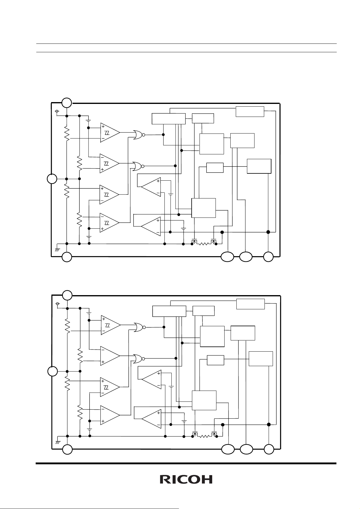
BLOCK DIAGRAMS
A/ D/ E/ F version
VDD
VD1U
O
scillator
R5460x
DS Circuit
Counter
Vc
VSS
C version
VDD
Logic
Circuit
Delay
VD2U
Level
Shift
Short
Detector
VD4
VD1L
Logic
Circuit
VD2L
VD3
OUT COUT
D
V-
DS Circuit
VD1U
O
scillator
Counter
Logic
Circuit
Delay
VD2U
Level
Shift
Short
Detector
Vc
VD4
VD1L
Logic
Circuit
VSS
VD2L
VD3
OUT COUT
D
V-
3
R5460x
SELECTION GUIDE
In the R5460xxxxxx Series, input threshold of over-charge, over-discharge, excess discharge current, and the
package and taping can be designated.
Part Number is designated as follows:
R5460x xxxxx-xx ← Part Number
↑ ↑ ↑↑ ↑
a b c d e
Code Contents
a Package Type N: SOT-23-6 K:DFN(PLP)1820-6
b
c Designation of Output delay option of over-charge and excess discharge-current.
d Designation of version symbols
e
Serial Number for the R5402 Series designating input threshold for over-charge,
over-discharge, excess discharge-current detectors.
Taping Type: TR (refer to Taping Specification)
PIN CONFIGURATIONS
SOT-23-6 DFN(PLP)1820-6
6
5
4
6
5
4
4
mark side
1
mark side
2
1
2
3
3
PIN DESCRIPTIONS
R5460x
Pin No.
Symbol
Description
SOT23-6 PLP1820-6
1
2
3
4
5
6
3
1
2
6
5
4
DOUT
COUT
V-
VC
VDD
VSS
The backside tab of DFN(PLP)1820-6 package is connected to the substrate level. (V
Output pin of over-discharge detection, CMOS output
Output pin of over-charge detection, CMOS output
Pin for charger negative input
Input Pin of the center voltage between two-cell
Power supply pin, the substrate voltage level of the IC.
Vss pin. Ground pin for the IC
DD) Note that avoiding
short with other level.
ABSOLUTE MAXIMUM RATINGS
Symbol
VDD
Vc
V-
VC
OUT
VD
OUT
PD
Topt
Ts tg
Supply voltage
Input voltage
Center pin voltage between two-cell
Charger negative input V- pin
Output voltage
C
OUT pin
D
OUT pin
Power dissipation
Operating temperature range
Storage temperature range
*Note: Exposure to the condition exceeded Absolute Maximum Ratings may cause the permanent damages
and affects the reliability and safety of both device and systems using the device.
The functional operations cannot be guaranteed beyond specified values in the Recommended
conditions.
Item
Ratings
-0.3 to 12
V
SS -0.3 to VDD+0.3
V
DD -30 to VDD+0.3
DD -30 to VDD + 0.3
V
V
SS -0.3 to VDD + 0.3
-40 to 85
-55 to 125
150
Unit
V
V
V
V
mW
°C
°C
5
R5460x
ELECTRICAL CHARACTERISTICS
R5460x2xxAA/AD/AE version Unless otherwise specified, Topt=25°C
Symbol Item Conditions Min. Typ. Max. Unit Note1
VDD1
Vst
VDET1U
VREL1U
tV
tV
V
DET1L
V
REL1L
VDET2U
V
REL2U
tVDET2
tVREL2
VDET2L
V
REL2L
VDET3
tVDET3
tVREL3
VDET4
tVDET4
tVREL4
Vshort Short protection voltage VDD-Vc=Vc-Vss=3.2V 0.7 1.1 1.5 V F
tshort Output Delay of Short protection
Rshort
VDS
VOL1
VOH1
VOL2
VOH2
Operating input voltage Voltage defined as V
Minimum operating Voltage
for 0V charging
CELL1 Over-charge threshold
CELL1 Over-charge
released voltage
Output delay of over-charge V
DET1
Output delay of release from
REL1
over-charge
CELL2 Over-charge detector
threshold
CELL2 Over-charge released voltage
CELL1 Over-discharge threshold
CELL1 Released Voltage from
Over-discharge
Output delay of over-discharge V
Output delay of release from
over-discharge
CELL2 Over-discharge threshold
CELL2 Released Voltage from
Over-discharge
Excess discharge-current
Threshold
Output delay of excess discharge
current
Output delay of release from
excess discharge-current
Excess charge-current threshold
Output delay of excess charge-current
Output delay of release from
excess charge-current
Reset resistance for Excess
discharge-current protection
Delay Shortening Mode input voltage V
Nch ON voltage of C
Pch ON voltage of C
Nch ON voltage of D
Pch ON voltage of D
Supply current V
IDD
Standby current V
IS
*Note 1
OUT Iol=50µA VDD-Vc=Vc-Vss=4.5V 0.4 0.5 V H
OUT Ioh=-50µA VDD-Vc=Vc-Vss=3.2V 6.8 7.4 V I
OUT Iol=50µA VDD-Vc=Vc-Vss=1.9V 0.2 0.5 V J
OUT Ioh=-50µA, VDD-Vc=Vc-Vss=3.2V 6.8 7.4 V K
Voltage defined as V
DD-Vss=0V
V
Detect rising edge of supply
Voltage
R1=330Ω (Topt=-5 to 55°C)
R1=330Ω
DD=3.2V to 4.5V, Vc-Vss=3.2V
DD=4.5V to 3.2V, Vc-Vss=3.2V 11 16 21 ms B
V
Detect rising edge of supply
voltage
R2=330Ω (Topt=-5 to 55°C)
R2=330Ω
Detect falling edge of supply
voltage
Detect rising edge of supply
voltage
DD=3.2V to 1.9V, Vc-Vss=3.2V 89 128 167 ms D
DD=1.9V to 3.2V, Vc-Vss=3.2V 0.7 1.2 1.7 ms D
V
Detect falling edge of supply
voltage
Detect rising edge of supply
voltage
Detect rising edge of 'V-' pin
voltage
V
DD-Vc=Vc-Vss=3.2V,
V-=0V to 0.5V
V
DD-Vc=Vc-Vss=3.2V,
V-=3V to 0V
Detect falling edge of 'V-' pin
voltage
DD-Vc=Vc-Vss=3.2V,
V
V-=0V to -1V
V
DD-Vc=Vc-Vss=3.2V,
V-=-1V to 0V
DD-Vc=Vc-Vss=3.2V,
V
V-=0V to 6.4V
DD-Vc=Vc-Vss=3.2V, V-=1V 25 40 75
V
DD-Vc=Vc-Vss=4.0V -2.2 -1.6 -1.0 V G
DD-Vc=Vc-Vss=3.2V, V-=0V 4.0 8.0 µA L
DD-Vc=Vc-Vss=1.9V 1.2 2.0 µA L
R1=330Ω
R2=330Ω
*Note: We compensate for this characteristic related to temperature by laser-trim, however, this specification
is guaranteed by design, not production tested.
*Note2: Indicates test circuits shown in 19-20 page.
DD-Vss 1.5 10.0 V A
DD-V-
*Note3
*Note3
1.8 V A
VDET1U
-0.025
VDET1U
VDET1U
-0.030
VDET1U
VREL1U-
0.050
VREL1U VREL1U+
0.7
VDET1L-
0.025
VDET1L
VDET1L
-0.030
VDET1L
VREL1L
-0.05
VREL1L VREL1L
VDET2U
×
0.975
VDET2U VDET2U
VREL2U
×
0.975
VREL2U VREL2U
VDET2L
×
0.975
VDET2L VDET2L
VREL2L
×
0.975
VREL2L VREL2L
VDET3
-0.015
8 12 16 ms F
0.7 1.2 1.7 ms F
-0.44 -0.40 -0.36
-0.23 -0.20 -0.17
-0.13 -0.10 -0.07
5 8 11 ms G
0.7 1.2 1.7 ms G
150 300 500 µs F
VDET3 VDET3
VDET1U
+0.025
V
VDET1U
+0.030
0.050
1.0 1.3 s B
VDET1L
+0.025
VDET1L
+0.030
+0.05
×
1.025
×
1.025
×
1.025
×
1.025
+0.015
V
V B
V
V
V C
V D
V D
V E
V E
V F
V G
kΩ
B
B
C
C
F
6
R5460x
R5460x2xxAC version Unless otherwise specified, Topt=25°C
Symbol Item Conditions Min. Typ. Max. Unit Note1
VDD1
Vst
VDET1U
VREL1U
tV
tV
V
DET1L
V
REL1L
VDET2U
tVDET2
tVREL2
VDET2L
VDET3
tVDET3
tVREL3
VDET4
tVDET4
tVREL4
Vshort Short protection voltage VDD-Vc=Vc-Vss=3.2V 0.7 1.1 1.5 V F
tshort Output Delay of Short protection
Rshort
VDS
VOL1
VOH1
VOL2
VOH2
Operating input voltage Voltage defined as V
Minimum operating Voltage
for 0V charging
CELL1 Over-charge threshold
CELL1 Over-charge
released voltage
Output delay of over-charge V
DET1
Output delay of release from
REL1
over-charge
CELL2 Over-charge detector
threshold
CELL2 Over-charge released voltage
CELL1 Over-discharge threshold
Output delay of over-discharge V
Output delay of release from
over-discharge
CELL2 Over-discharge threshold
Excess discharge-current
Threshold
Output delay of excess discharge
current
Output delay of release from
excess discharge-current
Excess charge-current threshold
Output delay of excess charge-current
Output delay of release from
excess charge-current
Reset resistance for Excess
discharge-current protection
Delay Shortening Mode input voltage V
Nch ON voltage of C
Pch ON voltage of C
Nch ON voltage of D
Pch ON voltage of D
Supply current V
IDD
Standby current V
IS
*Note 1
OUT Iol=50µA VDD-Vc=Vc-Vss=4.5V 0.4 0.5 V H
OUT Ioh=-50µA VDD-Vc=Vc-Vss=3.2V 6.8 7.4 V I
OUT Iol=50µA VDD-Vc=Vc-Vss=1.9V 0.2 0.5 V J
OUT Ioh=-50µA, VDD-Vc=Vc-Vss=3.2V 6.8 7.4 V K
Voltage defined as V
DD-Vss=0V
V
Detect rising edge of supply
Voltage
R1=330Ω (Topt=-5 to 55°C)
R1=330Ω
DD=3.2V to 4.5V, Vc-Vss=3.2V
DD=4.5V to 3.2V, Vc-Vss=3.2V 11 16 21 ms B
V
Detect rising edge of supply
voltage
R2=330Ω (Topt=-5 to 55°C)
R2=330Ω
Detect falling edge of supply
voltage
DD=3.2V to 1.9V, Vc-Vss=3.2V 89 128 167 ms D
DD=1.9V to 3.2V, Vc-Vss=3.2V 0.7 1.2 1.7 ms D
V
Detect falling edge of supply
voltage
Detect rising edge of 'V-' pin
voltage
V
DD-Vc=Vc-Vss=3.2V,
V-=0V to 0.5V
V
DD-Vc=Vc-Vss=3.2V,
V-=3V to 0V
Detect falling edge of 'V-' pin
voltage
DD-Vc=Vc-Vss=3.2V,
V
V-=0V to -1V
DD-Vc=Vc-Vss=3.2V,
V
V-=-1V to 0V
V
DD-Vc=Vc-Vss=3.2V,
V-=0V to 6.4V
DD-Vc=Vc-Vss=3.2V, V-=1V 25 40 75
V
DD-Vc=Vc-Vss=4.0V -2.2 -1.6 -1.0 V G
DD-Vc=Vc-Vss=3.2V, V-=0V 4.0 8.0 µA L
DD-Vc=Vc-Vss=1.9V 0.1 µA L
R1=330Ω
R2=330Ω
*Note: We compensate for this characteristic related to temperature by laser-trim, however, this specification
is guaranteed by design, not production tested.
*Note2: Indicates test circuits shown in 19-20 page.
DD-Vss 1.5 10.0 V A
DD-V-
*Note3
*Note3
1.8 V A
VDET1U
-0.025
VDET1U
VDET1U
-0.030
VREL1U-
0.7
VDET1L-
VDET1L
-0.030
VREL1L
VDET2U
×
VDET2L
×
VDET3
-0.015
8 12 16 ms F
0.7 1.2 1.7 ms F
-0.44 -0.40 -0.36
-0.23 -0.20 -0.17
-0.13 -0.10 -0.07
5 8 11 ms G
0.7 1.2 1.7 ms G
150 300 500 µs F
0.050
0.025
-0.05
0.975
0.975
VDET1U
VREL1U VREL1U+
VDET1L
VDET1L
VREL1L VREL1L
VDET2U VDET2U
VDET2L VDET2L
VDET3 VDET3
VDET1U
+0.025
V
VDET1U
+0.030
0.050
1.0 1.3 s B
VDET1L
+0.025
VDET1L
+0.030
+0.05
×
1.025
×
1.025
+0.015
V
V B
V
V
V C
V D
V E
V F
V G
kΩ
B
B
C
C
F
7
R5460x
R5460x2xxAF version Unless otherwise specified, Topt=25°C
Symbol Item Conditions Min. Typ. Max. Unit Note1
VDD1
Vst
VDET1U
VREL1U
tV
tV
V
DET1L
V
REL1L
VDET2U
V
REL2U
tVDET2
tVREL2
VDET2L
V
REL2L
VDET3
tVDET3
tVREL3
VDET4
tVDET4
tVREL4
Vshort Short protection voltage VDD-Vc=Vc-Vss=3.2V 0.7 1.1 1.5 V F
tshort Output Delay of Short protection
Rshort
VDS
VOL1
VOH1
VOL2
VOH2
Operating input voltage Voltage defined as V
Minimum operating Voltage
for 0V charging
CELL1 Over-charge threshold
CELL1 Over-charge
released voltage
Output delay of over-charge V
DET1
Output delay of release from
REL1
over-charge
CELL2 Over-charge detector
threshold
CELL2 Over-charge released voltage
CELL1 Over-discharge threshold
CELL1 Released Voltage from
Over-discharge
Output delay of over-discharge V
Output delay of release from
over-discharge
CELL2 Over-discharge threshold
CELL2 Released Voltage from
Over-discharge
Excess discharge-current
Threshold
Output delay of excess discharge
current
Output delay of release from
excess discharge-current
Excess charge-current threshold
Output delay of excess charge-current
Output delay of release from
excess charge-current
Reset resistance for Excess
discharge-current protection
Delay Shortening Mode input voltage V
Nch ON voltage of C
Pch ON voltage of C
Nch ON voltage of D
Pch ON voltage of D
Supply current V
IDD
Standby current V
IS
*Note 1
OUT Iol=50µA VDD-Vc=Vc-Vss=4.5V 0.4 0.5 V H
OUT Ioh=-50µA VDD-Vc=Vc-Vss=3.2V 6.8 7.4 V I
OUT Iol=50µA VDD-Vc=Vc-Vss=1.9V 0.2 0.5 V J
OUT Ioh=-50µA, VDD-Vc=Vc-Vss=3.2V 6.8 7.4 V K
Voltage defined as V
DD-Vss=0V
V
Detect rising edge of supply
Voltage
R1=330Ω (Topt=-5 to 55°C)
R1=330Ω
DD=3.2V to 4.5V, Vc-Vss=3.2V
DD=4.5V to 3.2V, Vc-Vss=3.2V 11 16 21 ms B
V
Detect rising edge of supply
voltage
R2=330Ω (Topt=-5 to 55°C)
R2=330Ω
Detect falling edge of supply
voltage
Detect rising edge of supply
voltage
DD=3.2V to 1.9V, Vc-Vss=3.2V 89 128 167 ms D
DD=1.9V to 3.2V, Vc-Vss=3.2V 0.7 1.2 1.7 ms D
V
Detect falling edge of supply
voltage
Detect rising edge of supply
voltage
Detect rising edge of 'V-' pin
voltage
V
DD-Vc=Vc-Vss=3.2V,
V-=0V to 0.5V
V
DD-Vc=Vc-Vss=3.2V,
V-=3V to 0V
Detect falling edge of 'V-' pin
voltage
DD-Vc=Vc-Vss=3.2V,
V
V-=0V to -1V
V
DD-Vc=Vc-Vss=3.2V,
V-=-1V to 0V
DD-Vc=Vc-Vss=3.2V,
V
V-=0V to 6.4V
DD-Vc=Vc-Vss=3.2V, V-=1V 25 40 75
V
DD-Vc=Vc-Vss=4.0V -2.2 -1.6 -1.0 V G
DD-Vc=Vc-Vss=3.2V, V-=0V 4.0 8.0 µA L
DD-Vc=Vc-Vss=1.9V 0.1 µA L
R1=330Ω
R2=330Ω
*Note: We compensate for this characteristic related to temperature by laser-trim, however, this specification
is guaranteed by design, not production tested.
*Note2: Indicates test circuits shown in 19-20 page.
DD-Vss 1.5 10.0 V A
DD-V-
*Note3
*Note3
1.8 V A
VDET1U
-0.025
VDET1U
VDET1U
-0.030
VDET1U
VREL1U-
0.050
VREL1U VREL1U+
0.7
VDET1L-
0.025
VDET1L
VDET1L
-0.030
VDET1L
VREL1L
-0.05
VREL1L VREL1L
VDET2U
×
0.975
VDET2U VDET2U
VREL2U
×
0.975
VREL2U VREL2U
VDET2L
×
0.975
VDET2L VDET2L
VREL2L
×
0.975
VREL2L VREL2L
VDET3
-0.015
8 12 16 ms F
0.7 1.2 1.7 ms F
-0.44 -0.40 -0.36
-0.23 -0.20 -0.17
-0.13 -0.10 -0.07
5 8 11 ms G
0.7 1.2 1.7 ms G
150 300 500 µs F
VDET3 VDET3
VDET1U
+0.025
V
VDET1U
+0.030
0.050
1.0 1.3 s B
VDET1L
+0.025
VDET1L
+0.030
+0.05
×
1.025
×
1.025
×
1.025
×
1.025
+0.015
V
V B
V
V
V C
V D
V D
V E
V E
V F
V G
kΩ
B
B
C
C
F
8

OPERATION
VDET1U,VDET1L / Over-Charge Detectors
R5460x
The VDET1U and VDET1L monitor the voltage between VDD pin and V
voltage between V
pin and VSS pin (the voltage of Cell2), if either voltage becomes equal or more than the
C
pin (the voltage of Cell1) and the
C
over-charge detector threshold, the over-charge is detected, and an external charge control Nch MOSFET
turns off with C
OUT pin being at "L" level.
VDET1U is the detector of Cell1, and the VDET1L is the detector of Cell2.
To reset the over-charge and make the C
OUT pin level to "H" again after detecting over-charge, in such
conditions that a time when the both Cell1 and Cell2 are down to a level lower than over-charge voltage, by
connecting a kind of load to V
of C
OUT pin becomes "H", and it makes an external Nch MOSFET turn on, and charge cycle is available. In
DD after disconnecting a charger from the battery pack. Then, the output voltage
other words, once over-charge is detected, even if the supply voltage becomes low enough, if a charger is
continuously connected to the battery pack, recharge is not possible. Therefore this over-charge detector has
no hysteresis. To judge whether or not load is connected, the built-in excess-discharge current detector is
used. By connecting some load, V- pin voltage becomes equal or more than excess-discharge current
detector threshold, and reset the over-charge detecting state.
Further, either or both voltage of Cell1 and Cell2 is higher than the over-charge detector threshold, if a
charger is removed and some load is connected, C
the parasitic diode of the external charge control Nch MOSFET. After that, when the V
lower than the over-charge detector threshold, C
OUT outputs “L”, however, load current can flow through
DD pin voltage becomes
OUT becomes “H”.
Internal fixed output delay times for over-charge detection and release from over-charge exist. If either or
both of the voltage of Cell1 or Cell2 keeps its level more than the over-charge detector threshold, and output
delay time passes, over-charge voltage is detected. Even when the voltage of Cell1 or Cell2 pin level becomes
equal or higher level than V
threshold
within a time period of the output delay time, the over-charge is not detected. Besides, after
DET1 if these voltages would be back to a level lower than the over-charge detector
detecting over-charge, while the both of Cell1 and Cell2 voltages are lower than the over-charge detector
threshold, even if a charger is removed and a load is connected, if the voltage is recovered within output delay
time of release from over-charge, over-charge state is not released.
A level shifter incorporated in a buffer driver for the C
voltage and the "H" level of C
OUT pin is set to VDD voltage with CMOS buffer.
OUT pin makes the "L" level of COUT pin to the V - pin
VDET2U,VDET2L / Over-Discharge Detectors
The VDET2U and VDET2L monitor the voltage between VDD pin and VC pin (Cell1 voltage) and the voltage
between V
C pin and VSS pin (Cell2 Voltage). When either of the cell1 or cell2 voltage becomes equal or less
than the over-discharge detector threshold, the over-discharge is detected and discharge stops by the
external discharge control Nch MOSFET turning off with the D
OUT pin being at "L" level.
The conditions to release over-discharge voltage detector after detecting over-discharge voltage are as
follows:
A/D versions: after connecting a charger, when the cell voltage becomes higher than over-discharge
detector threshold or, without connecting charger, when the cell voltage becomes equal or higher than
over-discharge released voltage.
C version: after connecting a charger, when the cell voltage becomes higher than over-discharge detector
threshold voltage.
E version: whether connecting a charger, or not, when the cell voltage becomes higher than released voltage
from over-discharge.
F version: after connecting a charger, when the cell voltage becomes higher than released voltage from
over-discharge.
In case that connecting a charger, for A/C/D versions, there is no hysteresis for over-discharge detector.
For E/F versions, even if a charger is connected to the battery pack, the hysteresis of over-discharge
9

R5460x
detector exists.
When a cell voltage equals to zero, if the voltage of a charger is equal or more than 0V-charge minimum
voltage (Vst), C
The output delay time for over-discharge detect is fixed internally. Even if the voltage of Cell1 or Cell2 is
down to equal or lower than the over-discharge detector threshold, if the voltage of Cell1 or Cell2 would be
back to a level higher than the over-discharge detector threshold within a time period of the output delay time,
the over-discharge is not detected. Output delay time for release from over-discharge is also set.
After detecting over-discharge, supply current would be reduced and be into standby by halting unnecessary
circuits and consumption current of the IC itself is made as small as possible.
C version: after detecting over-discharge, all the circuits are halted and the R5460 will be into standby mode.
Others: after detecting over-discharge, whole circuits except over-discharge released detector function are
halted, and the R5460 will be into standby mode.
The output type of D
VDET3 /Excess discharge-current Detector, Short Circuit Protector
Both of the excess current detector and short circuit protection can work when the both of control FETs are in
"ON" state.
When the V- pin voltage is up to a value between the short protection voltage Vshort /V
discharge-current threshold V
makes the short circuit protector enabled. This leads the external discharge control Nch MOSFET turns off
with the D
An output delay time for the excess discharge-current detector is internally fixed.
A quick recovery of V- pin level from a value between Vshort and V
discharge control FET staying "H" state. Output delay time for Release from excess discharge-current
detection is also set.
When the short circuit protector is enabled, the D
The V - pin has a built-in pull-down resistor to the Vss pin, that is, the resistance to release from
excess-discharge current.
After an excess discharge-current or short circuit protection is detected, removing a cause of excess
discharge-current or external short circuit makes an external discharge control FET to an "ON" state
automatically with the V- pin level being down to the V
reset resistor of excess discharge-current is off at normal state. Only when detecting excess discharge-current
or short circuit, the resistor is on.
Output delay time of excess discharge-current is set shorter than the delay time for over-discharge detector.
Therefore, if V
detected, the R5460xxxxxx is at excess discharge-current detection mode. By disconnecting a load, VDET3 is
automatically released from excess discharge-current.
VDET4/ Excess charge-current detector
OUT pin becomes "H" and a system is allowable to charge.
OUT pin is CMOS having "H" level of VDD and "L" level of VSS.
DD and excess
DET3, VDET3 operates and further soaring of V- pin voltage higher than Vshort
OUT pin being at "L" level.
DET3 within the delay time keeps the
OUT would be "L" and the delay time is also set.
SS level through the built-in pulled down resistor. The
DD voltage would be lower than VDET2 at the same time as the excess discharge-current is
When the battery pack is chargeable and discharge is also possible, VDET4 senses V- pin voltage. For
example, in case that a battery pack is charged by an inappropriate charger, an excess current flows, then the
voltage of V- pin becomes equal or less than excess charge-current detector threshold. Then, the output of
C
OUT becomes "L", and prevents from flowing excess current in the circuit by turning off the external Nch
MOSFET.
Output delay of excess charge current is internally fixed. Even the voltage level of V- pin becomes equal or
lower than the excess charge-current detector threshold, the voltage is higher than the VDET4 threshold
within the delay time, the excess charge current is not detected. Output delay for the release from excess
charge current is also set.
VDET4 can be released with disconnecting a charger and connecting a load.
10

R5460x
DS (Delay Shorten) function
Output delay time of over-charge, over-discharge, and release from those detecting modes can be shorter than
those setting value by forcing equal or less than the delay shortening mode voltage to V- pin when the C
“H”.
Operation against 2-Cell Unbalance
A/D/E version: If one of the cells detects over-charge and the output of COUT becomes "L" and keeps the status,
even if the other cell detects over-charge or over-discharge or short, the over-charge status is maintained and the
output of C
cell detects over-discharge and the former cell is released from over-charge, after the delay time of the released
from over-charge, the output of C
output of D
into the standby mode. (Supply current Max. 2.0μA)
C/F version: If one of the cells detect over-charge, and when the COUT becomes "L", even if the other cell
would detect over-discharge or short, the over-charge detector will be dominant and COUT keeps the "L" level. If
one of the cell detects the over-discharge, and when the DOUT becomes "L", in case that a charger is connected
to the battery pack and the other cell detects over-charge, the internal counter will start and after the delay time of
over-discharge detector, DOUT will become "H". After the delay time of over-charge release from when the
internal counter starts, COUT will be "L". If the over-discharge is detected, internal unnecessary circuits will be cut
off and the standby mode will be realized. (Standby current Max. 0.1μA)
In any versions, the external FETs do not turn off at the same time.
OUT keeps "L". If one of the cell detects over-charge and the output of COUT becomes "L", the other
OUT becomes "H", and after the delay time of detecting over-discharge, the
OUT becomes "L". After detecting over-discharge, A version halts internal unnecessary circuits and be
OUT is
11

R5460x
t
TIMING CHART
1) Timing diagram of Over-charge,Excess charge current
AA/AC/AD version
V
V
DD
C
V-
Connect Charger
V
-
V
DET1
C
V
REL1
Connect Load
Excess
Charge
Current
Charger Open
and Connec
Load
t
V
DET1
-
SS
V
REL1
V
t
DD
V
DET3
V
SS
V
DET4
V
t
REL1
t
4
t
REL1
V
DD
V
VDET
REL4
V
t
Charge Current
12
C OUT
Charge/
Discharge
Current
t
V
V
DET1
t
V-
DET1
t
0
t

d
C
E
AE/AF version
R5460x
V
V
DD
C
-
V-
V
Connect Charger
V
DET1 U
V -
C
V
REL 1U
V
DET1L
SS
V
REL1L
Connect Loa
xcess
Charge
Current
Disconnect
Charger
+ Connect Load
t
t
V
DD
V
DET3
SS
V
V
DET4
V
t REL1
V
DD
tVREL1
t
DET4
V
V
t
REL4
t
OUT
C
Charge Current
harge/
Discharge
Current
V
DET 1
t
V-
tVDET
1
t
0
t
13

R5460x
Ch
/Disch
E
2) Over-discharge, Excess discharge current, Short circuit
AA/AD version
V
REL2U
C
-
V
V-
V
-
V
DET2U
REL2L
V
SS
V
DET2L
V
DD
V
shor t
V
DET3
V
SS
V
DET4
DD
V
C
V
xcess
Connect Load
discharge
Connect Charger
current
Open
Short
Open
t
t
OUT
D
Charge Current
arge
ge Current
t
REL2
V
V
DD
Vss
t
V
DET2
t
V
DET2
t
V
REL2
DET3
t
V
t
REL3
V
t
V
tshor t
REL3
t
t
ar
0
t
14

C
Ch
C
C
C
Ov er-disc harge
C
AC version
R5460x
V
V
DD
- V
V
-
-
V
SS
V
V
V
V
DET2U
DET2L
V
V
short
DET3
V
DET4
V
DD
SS
DD
Connect Load
onnect
Charger
V
t
REL2
onnect
Load
Connect Charger
V
V
t
DET3
Current
Short
Open
Open
t
t
V
V
t REL3t REL2
t REL3
t
D
OUT
harge
Discharge
current
V
arge
Current
V
V
DET2
t
SS
t DET2
tshor t
t
0
t
15

R5460x
Ch
AE version
V
V
V-
DD
-
C
V SS
Connect
Connect Load
C
V
-
V
REL2U
V
DET2U
Charger
Ov er Discharge
Current
Open
Short
Open
t
V
REL2L
V
DET2L
t
V
DD
short
V
V
DET3
V
SS
V
DET4
OUT
D
arge
Current
Charge
/Di s ch arge
Current
V
Vss
DD
0
t
t
V
DET2
t
REL2
V
tVDET2
t
V
REL2
tVDET3
tVREL3
tshort
t
V
REL3
t
t
16

3) Operation with unbalanced cells
R5460x
AC version
VDET1L
VDD - VC
VC - VSS
V-
VREL1L
VDET2L
VDD
VDET3
VSS
VDET4
Connect Load
Connect Charger
Connect Load
Connect Charger
Open
t
t
COUT
DOUT
VDD
VSS
VDD
VSS
tVDET1 tVREL1
tVDET2 tVREL2
tVDET2
t
t
tVREL2
t
17

R5460x
V-
Vc
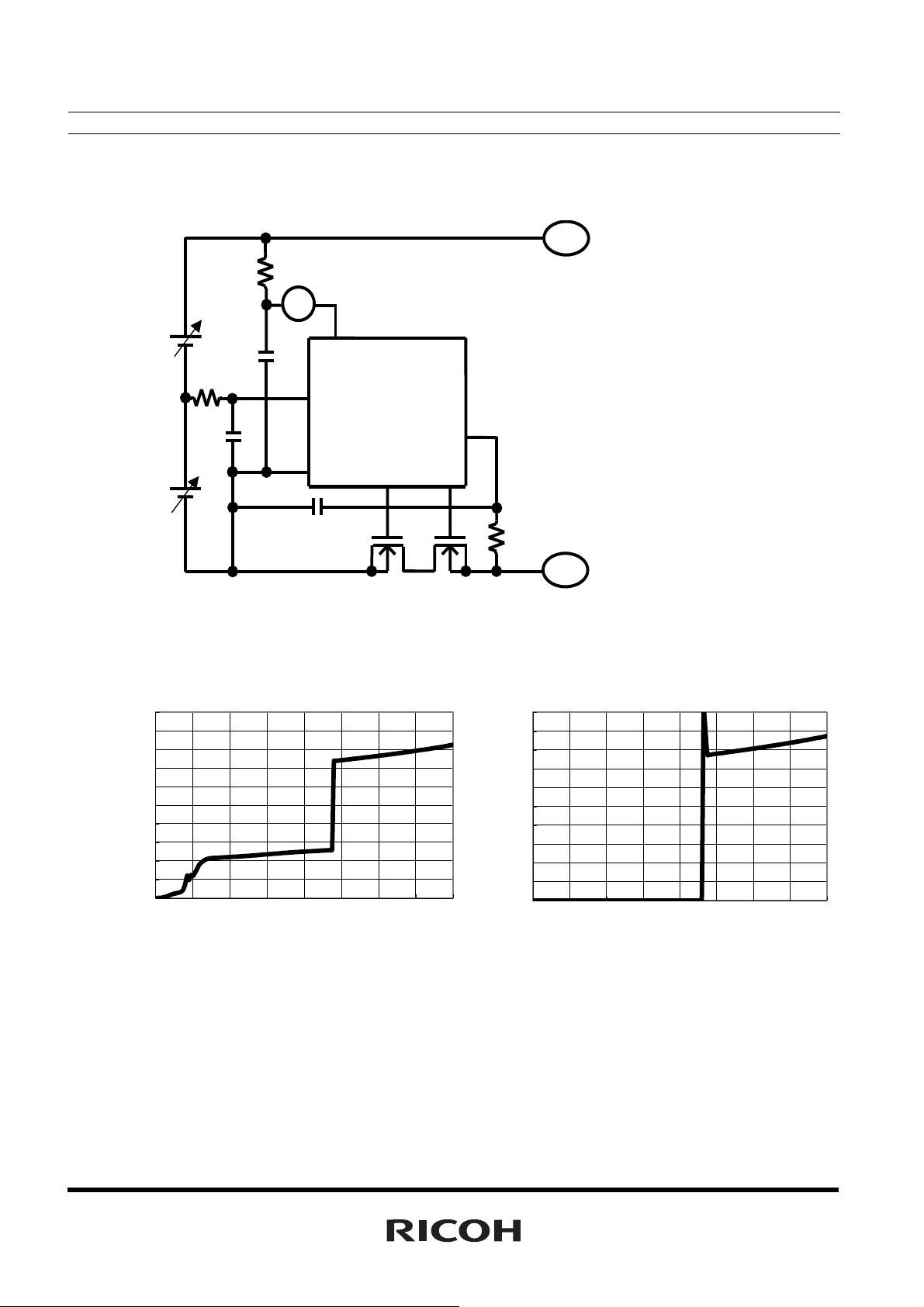
TYPICAL APPLICATION AND TECHNICAL NOTES
R1 330Ω
DD
V
C1
0.1μF
R2 330Ω
D
OUT
OUT
C
R3
1K Ω
R5460
C2
0.1μF
Vss
C3 0.01μF
TECHNICAL NOTES
R1, R2, C1 and C2 stabilize a supply voltage to the R5460xxxxxx. A recommended R1, R2 value is less than
1kΩ.
A larger value of R1 and R2 makes the detection voltage shift higher because of some conduction current in
the R5460xxxxxx.
To stabilize the operation, the value of C1 and C2 should be equal or more than 0.01μF.
R1 and R3 can operate also as parts for current limit circuit against reverse charge or applying a charger
with excess charging voltage beyond the absolute maximum rating of the R5460xxxxxx, the battery pack.
Small value of R1 and R3 may cause over-power consumption rating of power dissipation of the R5460xxxxx.
Thus, the total value of 'R1+R3' should be equal or more than 1kΩ.
If R3 value is set too large, after detecting over-discharge, release operation by connecting a charger may
be impossible, our recommendation value as R3 is 3kΩ or less.
To stabilize the operation of the IC, use 0.01μF or more capacitor as C3.
The typical application circuit diagram is just an example. This circuit performance largely depends on the
PCB layout and external components. In the actual application, fully evaluation is necessary.
Over-voltage and the over current beyond the absolute maximum rating should not be forced to the
protection IC and external components.
Ricoh cannot assume responsibility for use of any circuitry other than circuitry entirely embodied in a Ricoh
product. If technical notes are not complied with the circuit which is used Ricoh product, Ricoh is not
responsible for any damages and any accidents.
18

TEST CIRCUITS
A
V
DD
E
R5460x
V
DD
B
C
V
V
V-
VSS
V
DD
V
VC
VSS
V-
V
DD
DOUT
C
OUT
V
OSCILLOSCOPE
V
C
D
OUT
V
SS
V-
F
COUT
V
VDD
VC
DOUT
V-
A
V
SS
G
V
DD
D
VC
C
V
OUT
VSS
V-
V
V
DD
V
H
VC
D
OUT
VSS
V-
VC
V-
V
VC
V
V-
DD
SS
COUT
V
SS
C
OUT
A
V
19

R5460x
I
DD
V
C
V
C
OUT
A
V
SS
V
V-
J
DD
V
C
V
OUT
D
SS
V
A
V
V-
K
DD
V
D
OUT
A
C
V
V
20
V
V-
SS
L
A
DD
V
C
V
V-
SS
V

R5460x
TYPICAL CHARACTERISTICS (Part 1)
1) Minimum Operating Voltage for 0V Cell Charging 2) Over-charge voltage threshold (Cell1) vs. Temperature
R5460x201AC R5460x201AC
2.0
1.8
1.6
1.4
1.2
1.0
VST(V)
0.8
0.6
0.4
0.2
0.0
-50 -25 0 25 50 75 100
VDD=VSS=0V
Temperature Topt (°C)
4.375
4.370
V)
4.365
4.360
DET1U(
4.355
4.350
4.345
4.340
4.335
Over-charge voltage
4.330
threshold Cell1 V
4.325
-60 -40 -20 0 20 40 60 80 100
Vc-Vss=3.5V
Temperature Topt(°C)
3) Over-Charge Voltage Threshold (Cell2) vs. Temperature 4)Release Voltage from Over-charge (Cell1) vs.
Temperature
R5460x201AC R5460x201AC
4.40
4.39
4.38
4.37
4.36
)
V
4.35
(
4.34
4.33
VDET1L
4.32
4.31
4.30
4.29
4.28
-50 -25 0 25 50 75 100
VDD-VC=3.5V
Temperature Topt(°C)
4.30
)
V
4.25
(
4.20
4.15
4.10
4.05
voltage detect Cell1 VREL1U
Release Voltage from Over-charge
4.00
-60 -40 -20 0 20 40 60 80 100
Vc-Vss=3.5V
Tempperature Topt
(°C)
21

R5460x
5) Release Voltage from Over-charge (Cell2) vs. 6) Output Delay of Over-charge Detector vs. Temperature
Temperature
R5460x201AC R5460x201AC
4.30
4.25
V)
4.20
REL1L(
4.15
4.10
charge Cell2 V
4.05
Release Voltage from Over-
4.00
-60 -40 -20 0 20 40 60 80 100
7) Output Delay of Release from Over-charge vs. Temperature 8) Over-discharge Detector Threshold (Cell1) vs. Temperature
VDD-VC=3.5V
Temperature Topt(°C)
Over-charge Detector Output
1.8
1.6
1.4
(s)
1.2
DET1
1.0
0.8
0.6
0.4
Delay Time tV
0.2
0.0
-60 -40 -20 0 20 40 60 80 100
VC-VSS=3.5V
Temperature Topt(°C)
R5460x201AC R5460x201AC
32
28
(ms)
24
REL1
20
16
12
8
from Over-charge tV
Output Delay Time of Release
4
-60 -40 -20 0 20 40 60 80 100
Vc-Vss=3.5V
Temperature Topt(°C)
2.40
2.38
(V)
2.35
DET2U
2.33
2.30
2.28
2.25
Over-discharge Detector
Threshold Cell1 V
2.23
2.20
-60 -40 -20 0 20 40 60 80 100
Vc-Vss=3.5V
Temperature Topt(°C)
9) Over-discharge Detector Threshold (Cell2) vs. 10) Release Voltage from Over-discharge (Cell1) vs.
Temperature Temperature
R5460x201AC R5460x202AA
2.37
2.35
2.33
)
V
(
2.31
2.29
VDET2L
2.27
2.25
2.23
-50 -25 0 25 50 75 100
VDD-VC=3.5V
Temperature Topt(°C)
3.20
3.15
3.10
REL2
3.05
3.00
2.95
2.90
discharge Cell1 V
2.85
ReleaseVoltage from Over-
2.80
-60 -40 -20 0 20 40 60 80 100
Vc-Vss=3.5V
Temperature Topt(°C)
22
R5460x
11) Release Voltage from Over-discharge (Cell2) vs. 12) Output Delay Time for Over-discharge vs.
Temperature
Temperature
R5460x202AA R5460x201AC
3.20
3.15
3.10
3.05
3.00
2.95
CELL2 (V)
2.90
2.85
Release from Over-discharge
2.80
-60 -40 -20 0 20 40 60 80 100
VDD-Vc=3.5V
Temperature Topt(°C)
13) Output Delay of Release from Over-discharge vs. Temperature 14) Excess discharge Current Detector Threshold vs. Temperature
250
225
200
ms)
175
150
DET2(
125
100
75
discharge tV
50
Output Delay Time of Over-
25
0
-60 -40 -20 0 20 40 60 80 100
Vc-Vss=3.5V
Temperature Topt(°C)
R5460x201AC R5460x201AC
2.6
2.4
2.2
2.0
1.8
1.6
(ms)
1.4
1.2
REL2
1.0
tV
0.8
0.6
Output Delay Time for
0.4
Release from Over-discharge
0.2
0.0
-60 -40 -20 0 20 40 60 80 100
Vc-Vss=3.5V
Temperature Topt(°C)
0.220
0.215
)
0.210
V
(
0.205
DET3
V
0.200
0.195
0.190
Threshold
0.185
Excess discharge Current Detector
0.180
-60 -40 -20 0 20 40 60 80 100
Temperature Topt(°C)
15) Output Delay Time for Excess discharge-current Detector vs. 16) Output Delay for Release from Excess discharge-current vs.
Temperature
Temperature
R5460x201AC R5460x201AC
20
18
DET3
15
13
)
10
ms
(
8
5
Output Delay Time for Excess
3
discharge-current Detector tV
0
-60 -40 -20 0 20 40 60 80 100
Temperature Topt(°C)
2.8
2.4
2.0
1.6
(ms)
REL3
1.2
tV
0.8
Excess discharge-current
0.4
Output Delay for Release from
0.0
-50 -25 0 25 50 75 100
Temperature Topt (°C)
23

R5460x
17) Short Detector Voltage Threshold vs. Temperature 18) Output Delay for Short Detector vs. Temperature
R5460x201AC R5460x201AC
1.8
1.6
1.4
1.2
1.0
0.8
0.6
VSHORT(V)
0.4
Short Detector Threshold
0.2
0.0
-50 -25 0 25 50 75 100
19) Release resistance from Excess-discharge current vs. 20) Excess-charge current Detector Threshold vs. Temperature
Temperature
VDD-VC=VC-VSS=3.5V
Temperature Topt (°C)
R5460x201AC R5460x201AC
80
75
70
65
60
55
50
45
40
35
30
25
discharge current RSHORT(kΩ)
Release Resistance from Excess-
20
15
21) Output Delay Time of Excess-charge current Detector Threshold 22) Output Delay Time for Release from Excess-charge current vs.
vs. Temperature Temperature
VDD-VC=VC-VSS=3.6V
-50 -25 0 25 50 75 100
Temperature Topt(°C)
R5460x201AC R5460x201AC
20
18
16
14
12
ms)
10
DET4(
8
tV
6
4
Excess charge current
Output Delay for detecting
2
0
-50 -25 0 25 50 75 100
Temperature Topt(°C)
600
550
500
450
400
350
SHORT(μs)
300
250
200
150
Detector T
100
Output Delay Time for Short
50
0
-60 -40 -20 0 20 40 60 80 100
Temperature Topt(°C)
-0.30
-0.32
-0.34
-0.36
(V)
-0.38
DET4
-0.40
-0.42
-0.44
Threshold V
-0.46
Excess Charge Current Detector
-0.48
-0.50
Output Delay for Release from
-60 -40 -20 0 20 40 60 80 100
2.8
2.4
2.0
1.6
(ms)
1.2
REL4
tV
0.8
0.4
Excess charge current detect
0.0
-50 -25 0 25 50 75 100
Temperature Topt(°C)
Temperature Topt (°C)
24

R5460x
d
(
)
23) Delay Shortening Mode Voltage vs. Temperature 24) Nch ON Voltage of COUT vs. Temperature
R5460x201AC R5460x201AC
Delay Shrtening Mode Threshol
-0.4
-0.6
-0.8
-1.0
-1.2
-1.4
V)
-1.6
DS (
-1.8
V
-2.0
-2.2
-2.4
-2.6
-2.8
-50 -25 0 25 50 75 100
Temperature Topt(°C)
)
OUT
V)
OL1(
V
Nch ON Voltage(C
VDD-VC=VC-VSS=4.5V, IOL=50μA
0.50
0.45
0.40
0.35
0.30
0.25
0.20
0.15
0.10
0.05
0.00
-50 -25 0 25 50 75 100
Temperature Topt (°C)
25) Pch ON Voltage of C
OUT vs. Temperature 26) Nch ON Voltage of DOUT vs. Temperature
R5460x201AC R5460x201AC
VDD-VC=VC-VSS=3.9V, IoH=-50μA
7.9
7.7
OUT
7.5
)
7.3
V
(
7.1
6.9
VOH1
6.7
Pch ON Voltage of C
6.5
6.3
-50 -25 0 25 50 75 100
Temperature Topt (°C)
27) Pch ON Voltage of D
Nch ON Voltage of DOUT
OUT vs. Temperature 28) Supply Current vs. Temperature
VDD-VC=VC-VSS=2V, IoL=50μA
0.50
0.45
0.40
0.35
0.30
0.25
0.20
VOL2(V)
0.15
0.10
0.05
0.00
-50 -25 0 25 50 75 100
Temperqture Topt (°C)
R5460x201AC R5460x201AC
VDD-VC=VC-VSS=3.9V、Dout・VSS=-50μA
8.3
8.1
OUT
7.9
7.7
7.5
V
7.3
7.1
VOH2
6.9
6.7
Pch On Voltage of D
6.5
6.3
-50 -25 0 25 50 75 100
Min=6.8V, Typ.=7.4V
Temperature (°C)
10
9
8
7
)
6
μA
5
(
Iss
4
3
2
1
0
-50 -25 0 25 50 75 100
VDD-VCC=VC-VSS=3.9V
Temperature Topt(°C)
25

R5460x
29) Standby Current vs. Temperature (Ver. A.) 30) Standby Current vs. Temperature (Ver. C.)
R5460X202AA
2.0
(VDD-Vc=Vc-Vss=2.0V)
1.8
1.6
1.4
1.2
1.0
0.8
0.6
0.4
Standby Current Istb(uA)
0.2
0.0
-50 -25 0 25 50 75 100
Temperature Topt(C)
Part 2 Delay Time dependence on V
DD
1) Delay Time for Over-charge detector vs. V
R5460x2xxAx
V-=0V,VDD=3.5V to 4.4V, 5.0V, 5.6V Vc-Vss =3.5V
[s]
1.2
DET1
1
0.8
0.6
0.4
0.2
0
Output delay of over-charge tV
4 4.5 5 5.5 6
DD
V
[V]
1.0
0.9
0.8
0.7
0.6
0.5
0.4
0.3
0.2
Standby Current Istb(μA)
0.1
0.0
-50 -25 0 25 50 75 100
DD 2) Delay Time for Release from Over-charge vs. VDD
V-=0V,VDD=4.5V to 3.2V,3.7V,4.0V,Vc-Vss=3.5V
18
16
14
12
[ms]
10
8
REL1
tV
6
4
from over-charge
2
Output delay of release
0
33.544.5
R5460x201AC
(VDD-VC=VC-VSS=2.0V)
Temperature Topt (°C)
R5460x2xxAx
DD
V
[V]
3) Output Delay of Over-discharge detector vs. VDD 4) Output Delay for Release from Over-discharge vs. VDD
26
R5460x2xxAx
V-=0V,VDD=3.5V to 2.2V,2.0V,1.5V,Vc-Vss=3.5V
140
120
[ms]
100
DET2
80
60
40
Output delay of over-
discharge tV
20
0
11.522.5
DD
V
[V]
V-=0V,VDD=2.2V to 2.5V,3.3V,4.2V Vc-Vss=3.5V
1.6
1.4
ms]
[
1.2
REL2
1
0.8
0.6
0.4
0.2
over-discharge tV
Output delay of release from
0
2 2.5 3 3.5 4 4.5
R5460x2xxAx
DD
[V]
V

R5460x
5) Output Delay for Excess Discharge Current 6) Output Delay for Release from Excess
Discharge
vs. V
DD Current Detect vs. VDD
R5460x2xxAx
VDD=2.4V,3.3V ,4.2V,Vc-Vss=3.5V,V-=0V to 0.5V
14
12
10
8
[ms]
6
DET3
tV
4
discharge current
2
Output delay of excess
0
2 2.5 3 3.5 4 4.5
DD
V
[V]
VDD=2.4V,3.3V ,4.2V Vc-Vss=3.5V V-=3.0V to 0V
1.4
1.2
1
0.8
[ms]
0.6
REL3
tV
0.4
0.2
excess discharge-current
Output delay of release from
0
22.533.544.5
R5460x2xxAx
DD
V
[V]
7) Delay Time for Excess Charge Current Detector 8) Delay Time for release from Excess charge
vs. V
VDD=2.4V, 3.3V, 4.2V Vc-Vss=3.5V V-=0V to -0.9V
DD current detect vs. VDD
R5460x2xxAx
9
8
[ms]
7
6
DET4
5
4
3
2
1
Output delay of excess
charge-current tV
0
22.533.544.5
VDD[V]
VDD=2.4V, 3.3V, 4.2V Vc-Vss=3.5V V-=-0.9V to 0V
1.4
1.2
1
0.8
[ms]
0.6
REL4
tV
0.4
0.2
Output delay of release
from excess charge-current
0
R5460x2xxAx
2 2.5 3 3.5 4 4.5
VDD[V]
9) Output Delay for Short vs. V
R5460x2xxAx
VDD=2.4V, 3.3V, 4.2V Vc-Vss=3.5V V-=0V to 1.5V
350
300
[μs]
250
200
SHORT
150
100
protection t
Output delay of short
50
0
22.533.544.5
DD
DD
[V]
V
27
R5460x
Part 3 Supply Current dependence on VDD
R1 330Ω
CELL1
R2 330
C2
0.1μF
Ω
A
C1
0.1μF
Vc
Vss
VDD
R5460
Test Circuit
V-
OUTDOUT
C
PACK+
CELL2
C3 0.01μF
R3
1K
Ω
PACK-
Supply Current vs. VDD
A version C version
5
4.5
4
(uA)
3.5
DD
3
2.5
2
1.5
1
Supply Current I
0.5
0
012345678
DD
(V)
V
5
4.5
4
(uA)
3.5
DD
3
2.5
2
1.5
1
Supply Current I
0.5
0
012345678
DD
(V)
V
28

R5460x
Part 4 Over-charge detector, Release voltage from Over-charge, Over-discharge detector, Release voltage
from Over-discharge dependence on External Resistance value
Test Circuit
PACK+
R1
CELL1
V
R2 330
C2
0.1μF
C1
Ω
0.1μF
Vc
Vss
DD
R5460
D
OUT
V-
C
OUT
CELL2
C3 0.01μF
R3
1K
Ω
PACK-
Over-charge Detector Threshold(VDET1) / Released Voltage from Over-discharge(VREL1) vs. R1
R5460x202AA
4.264
4.260
4.256
[V]
DET1
4.252
V
4.248
4.244
4.240
V
0 200 400 600 800 1000
V
DET1
REL1
R1[Ω]
4.064
4.060
4.056
4.052
4.048
4.044
4.040
[V]
REL1
V
[V]
DET1
V
4.361
4.359
4.357
4.355
4.353
4.351
4.349
4.347
4.345
4.343
4.341
0 200 400 600 800 1000
R5460x201AC
V
V
DET1
REL1
4.164
4.162
4.160
4.158
4.156
4.154
4.152
4.150
4.148
4.146
4.144
R1[Ω]
Over-discharge(VDET2) / Released from Over-charge Threshold(VREL2) vs. R1
2.405
2.400
[V]
2.395
DET2
V
2.390
2.385
R5460x202AA
V
0 200 400 600 800 1000
DET2
V
REL2
R1[Ω]
3.05
3.04
3.03
3.02
3.01
3.00
2.99
2.98
2.97
2.96
2.95
[V]
REL2
V
2.316
2.314
2.312
2.310
2.308
[V]
2.306
DET2
2.304
V
2.302
2.300
2.298
2.296
R5460x201AC
VDET2
VREL2
0 200 400 600 800 1000
R1[Ω]
2.50
2.46
2.42
2.38
2.34
2.30
[V]
REL2
V
[V]
REL1
V
29

R5460x
Part 5 Charger Voltage at Released from Over-discharge with a Charger dependence on R2
Test Circuit
PACK+
R1
330
Ω
CELL1
V
R2
C2
0.1μF
C1
330
0.1μF
Ω
Vc
Vss
DD
R5460
D
OUT
V-
C
OUT
CELL2
C3 0.01μF
R3
PACK-
Charger Voltage at Release from Over-discharge with a charger vs. R2
R5460x201AC
CELL1=4.25V,CELL2=4.25V
10
9
8
7
6
5
4
discharge[V]
3
2
Charger Voltage of Release from Over-
1
30
0
0123456789101112
R3[kΩ]

R5460x
A
A
A
A
A
A
F
A
F
A
A
F
C
F
F
F
R5460x CO DE L IST
Part No. VDET1(V) VREL1(V) VDET2(V) VREL2(V) VDET3(V) VDET4(V) tVDET1(s) tVDET2(ms) tVDET3(ms) tVDET4(ms) tSHORT(us) 0V Charge
R5460N201AC 4.350 4.150 2.300 - 0.200 -0.400 1 128 12 8 300 OK
R5460N202A
R5460N203A
R5460N204A
R5460N205A
R5460N206A
R5460N207A
R5460N207AE 4.350 4.150 2.300 3.000 0.200 -0.200 1 128 12 8 300 OK
R5460N207A
R5460N208A
R5460N208AE 4.250 4.050 2.400 3.000 0.200 -0.200 1 128 12 8 300 OK
R5460N208A
R5460N209AD 3.650 3.450 2.500 3.000 0.200 -0.200 1 128 12 8 300 OK
R5460N210AD 3.650 3.450 2.000 2.500 0.200 -0.200 1 128 12 8 300 OK
R5460N211A
R5460N212A
R5460N212AE 4.290 4.050 3.000 3.200 0.200 -0.200 1 128 12 8 300 OK
R5460N212A
R5460N213AD 3.900 3.450 2.000 2.500 0.200 -0.200 1 128 12 8 300 OK
R5460N214A
R5460N214AE 4.250 4.050 2.800 3.000 0.200 -0.200 1 128 12 8 300 OK
R5460N214A
R5460N215A
R5460N218A
R5460K201AC 4.350 4.150 2.300 - 0.200 -0.400 1 128 12 8 300 OK
R5460K202AA 4.250 4.050 2.400 3.000 0.150 -0.400 1 128 12 8 300 OK
R5460K203AA 4.350 4.150 2.300 3.000 0.200 -0.400 1 128 12 8 300 OK
R5460K204AA 4.350 4.150 2.300 3.000 0.150 -0.200 1 128 12 8 300 OK
R5460K205AA 4.250 4.050 2.400 3.000 0.100 -0.200 1 128 12 8 300 OK
R5460K206AA 4.290 4.050 2.900 3.100 0.150 -0.200 1 128 12 8 300 OK
R5460K207AA 4.350 4.150 2.300 3.000 0.200 -0.200 1 128 12 8 300 OK
R5460K208AA 4.250 4.050 2.400 3.000 0.200 -0.200 1 128 12 8 300 OK
R5460K209AD 3.650 3.450 2.500 3.000 0.200 -0.200 1 128 12 8 300 OK
R5460K210AD 3.650 3.450 2.000 2.500 0.200 -0.200 1 128 12 8 300 OK
R5460K211AA 4.250 4.050 3.000 3.200 0.150 -0.200 1 128 12 8 300 OK
R5460K213AD 3.900 3.450 2.000 2.500 0.200 -0.200 1 128 12 8 300 OK
R5460K214AC 4.250 4.050 2.800 3.000 0.200 -0.200 1 128 12 8 300 OK
(as of 2009/12/21)
4.250 4.050 2.400 3.000 0.150 -0.400 1 128 12 8 300 OK
4.350 4.150 2.300 3.000 0.200 -0.400 1 128 12 8 300 OK
4.350 4.150 2.300 3.000 0.150 -0.200 1 128 12 8 300 OK
4.250 4.050 2.400 3.000 0.100 -0.200 1 128 12 8 300 OK
4.290 4.050 2.900 3.100 0.150 -0.200 1 128 12 8 300 OK
4.350 4.150 2.300 3.000 0.200 -0.200 1 128 12 8 300 OK
4.350 4.150 2.300 3.000 0.200 -0.200 1 128 12 8 300 OK
4.250 4.050 2.400 3.000 0.200 -0.200 1 128 12 8 300 OK
4.250 4.050 2.400 3.000 0.200 -0.200 1 128 12 8 300 OK
4.250 4.050 3.000 3.200 0.150 -0.200 1 128 12 8 300 OK
4.290 4.050 3.000 3.200 0.200 -0.200 1 128 12 8 300 OK
4.290 4.050 3.000 3.200 0.200 -0.200 1 128 12 8 300 OK
4.250 4.050 2.800 3.000 0.200 -0.200 1 128 12 8 300 OK
4.250 4.050 2.800 3.000 0.200 -0.200 1 128 12 8 300 OK
4.300 4.100 3.200 3.400 0.150 -0.200 1 128 12 8 300 OK
4.250 4.050 2.800 3.000 0.200 -0.100 1 128 12 8 300 OK
R5460 x 2xx A x
Package Type Function Version
N : SOT23-6
K : PLP1820-6
A : Over-Charge = Auto-Release Over-Discharge = Auto Release
C : Over-Charge = Auto-Release Over-Discharge = Latch
D : Over-Charge = Auto-Release Over-Discharge = Auto Release VDET1U/L < 4.0V
E : Over-Charge = Auto-Release Over-Discharge = Auto Release ( No Hysteresis Cancellation )
F : Over-Charge = Auto-Release Over-Discharge = Latch ( Hysteresis )
Delay Time Version
Ver.
t
Vdet1(s)tVdet2(ms)tVdet3(ms)tVdet4(ms) tSHORT(us)
Voltage Version A 1 128 12 8 300
31
 Loading...