PRELIMINARY
’99.12.9
Li-Ion BATTERY PROTECTOR
R5422NxxxC/xxxE series
OUTLINE
n
The R5422NxxxC/E Series are pr otection ICs for over-charge/discharge of rechargeable one-cell Lithium-ion ( Li+ ) excess load
current, further include a short circuit protector for preventing large external short circuit current.
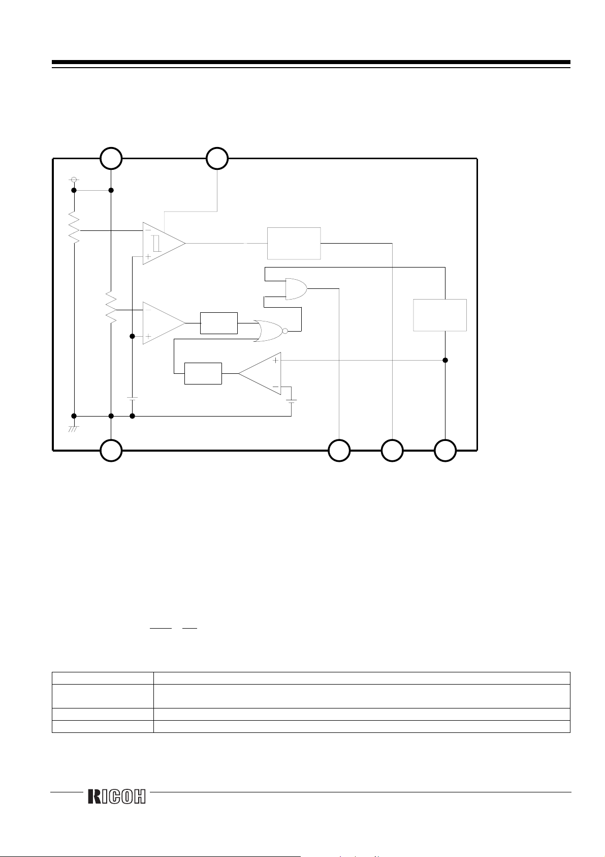
Each of these ICs is composed of three voltage detectors, a reference unit, a delay circuit, a short circuit protector, and a logic
DET1
circuit. When charging voltage crosses the detector threshold from a low value to a value higher than V
, the output of C
pin, the output of over-charge detector/VD1, switches to low level, charger's negative pin level after the delay time by setting an
OUT
external capacitor. After detecting over-charge the VD1 can be reset and the output of C
is coming down to a level lower than “V
the battery pack while the V
The output of D
OUT
pin, the output of over-discharge detector/VD2, switches to low level after internally fixed delay time passed,
DD
level is in between “V
REL1
”, or when a kind of loading is connected to VDD after a charger is disconnected from
DET1
” and “V
REL1
” in the R5422NxxxC/E version.
when discharging voltage crosses the detector threshold from a high value to a value lower than V
becomes high when the VDD voltage
DET2
.
After R5422NxxxC/E Series detect the over-discharge voltage, connect a charger to the battery pack, and when the battery
supply voltage becomes higher than the over-discharge detector threshold, VD2 is released and the voltage of D
OUT
“H” level.
An excess load current can be sensed and cut off after internally fixed delay time passed through the built in excess current
detector, VD3, with D
OUT
being enabled to low level. Once after detecting excess current, the VD3 is released and D
switches to high by detaching a battery pack from a load system.
Further, short circuit protector makes D
short circuit leads D
OUT
level to high. After detecting over-discharge, supply current will be kept extremely low by halt some
internal circuits operation. Output type of C
OUT
level to low immediately with external short circuit current and removing external
OUT
and D
OUT
is CMOS. 6-pin, SOT23-6 is available.
becomes
OUT
level
OUT
FEATURES
n
l High Voltage Process Technology Absolute Maximum Rating of Voltage level between VDD-V- 28v
l Low supply current....................................................Supply current Typ. 6.0µA
Standby current (detecting over-discharge) Typ. 0.1µA
l High accuracy detector threshold..............................Over-charge detector (Topt=25°C) ±25mV
(To pt = 0 to 50°C ) ±30 mV
Over-discharge detector ±2.5%
Excess current detector ±20mV
l Variety of detector threshold .....................................Over-charge detector threshold 4.0V - 4.5V step of 0.01V
Over-discharge detector threshold 2.0V - 3.0V step of 0.01V
l Built-in protection circuit..........................................Excess current protection 0.05V - 0.4V step of 0.01V
l Output delay of over-charge......................................Time delay at C=0.01µF tV
DET1
=75ms, tV
REL1
=20ms
l Output delay of over-discharge.................................Internally fixed TYP. 17ms
l Output delay of excess-current Internally fixed TYP. 10ms
l 2 Over-current modes Excess Current Mode / Short Mode
l Charging Available / non-available at 0V Cell Acceptable of 0V Cell C version
Non-acceptable of 0V Cell E version
l Small package............................................................SOT-23-6 / 6-pin
APPLICATIONS
n
l Li+ one-cell protector for battery pack
Rev. 0.01 - 1 -

BLOCK DIAGRAM
n
DD
V
5
Ct
4
Level
Shift
VD1
Short
Delay
Detector
VD2
Delay
VD3
6
231
Dout Cout V-Vss
SELECTION GUIDE
n
In the R5422Nxxxx Series, three of the input threshold for over-charge, over-discharge and excess current detectors can be
designated.
Part Number is designated as follows:
R5422N XXXX-XX
---
abc
Code Description
a
b Designation of versio n sy mbo ls
c Taping T y pe: TR (refer to Taping Specification)
Serial Number for the R5422N Series designating input threshold for over-charge, over-discharge
and excess current detectors as well as hysteresis range for over-charge detector.
¬Part Number
Rev. 0.01 - 2 -

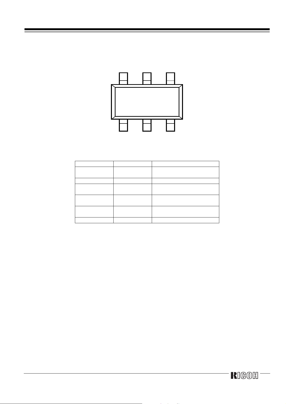
PIN CONFIGURATION
n
PIN DESCRIPTION
n
654
(mark side)
123
Pin No. Symbol Pin description
1D
2 V- Pin for charger ne gative input
3C
4Ct
5V
6V
OUT
OUT
DD
SS
Output of over-discharge
detection, CMOS output
Output of over-charge
detection, CMOS output
Pin for external capacitor
setting output delay of VD1
Power supply(Substrate voltage
level of the IC)
Ground(Gr ound pin of the IC)
Rev.0.01 - 3 -
 Loading...