How it Works
Log In / Sign Up
Buy Points
How it Works
FAQ
Contact Us
Questions and Suggestions
Users
Datasheet
Loading...
R
R3000
3
R3000F
4
R30070
R30120
R30337
R30410
R304100
R304120
R30420
R30440
R30460
R3047TC24x
R3047TC28x
R30480
R306100
R306120
R30620
R30640
R30660
R30680
R30720
R30740
R30760
R30A
R30B
R30D
R30G
R30J
R30K
R30M
R30N-3011-85-1012
R3111xxx1A-C
R3112x
R3114x
R3116x
R3117xxx1
R3117xxx2
R3117xxx3
R3117xxx4
R3118x
R3119N
2
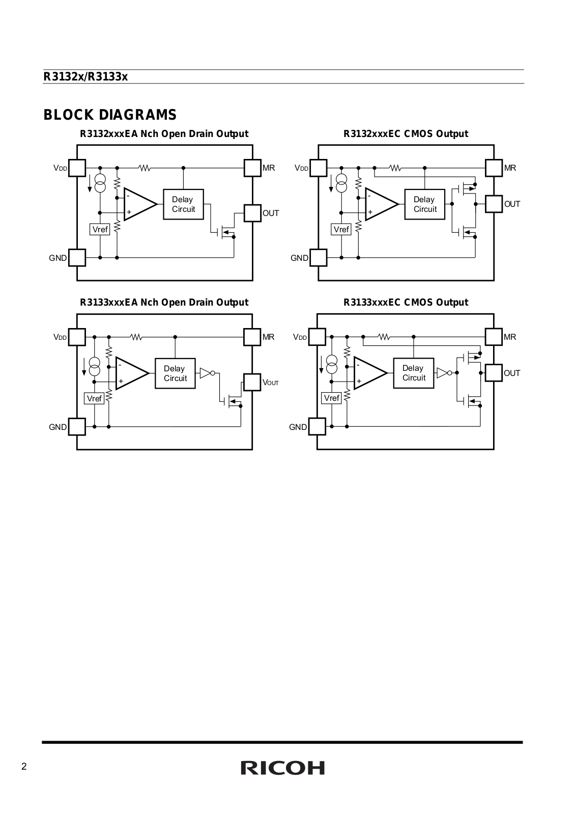
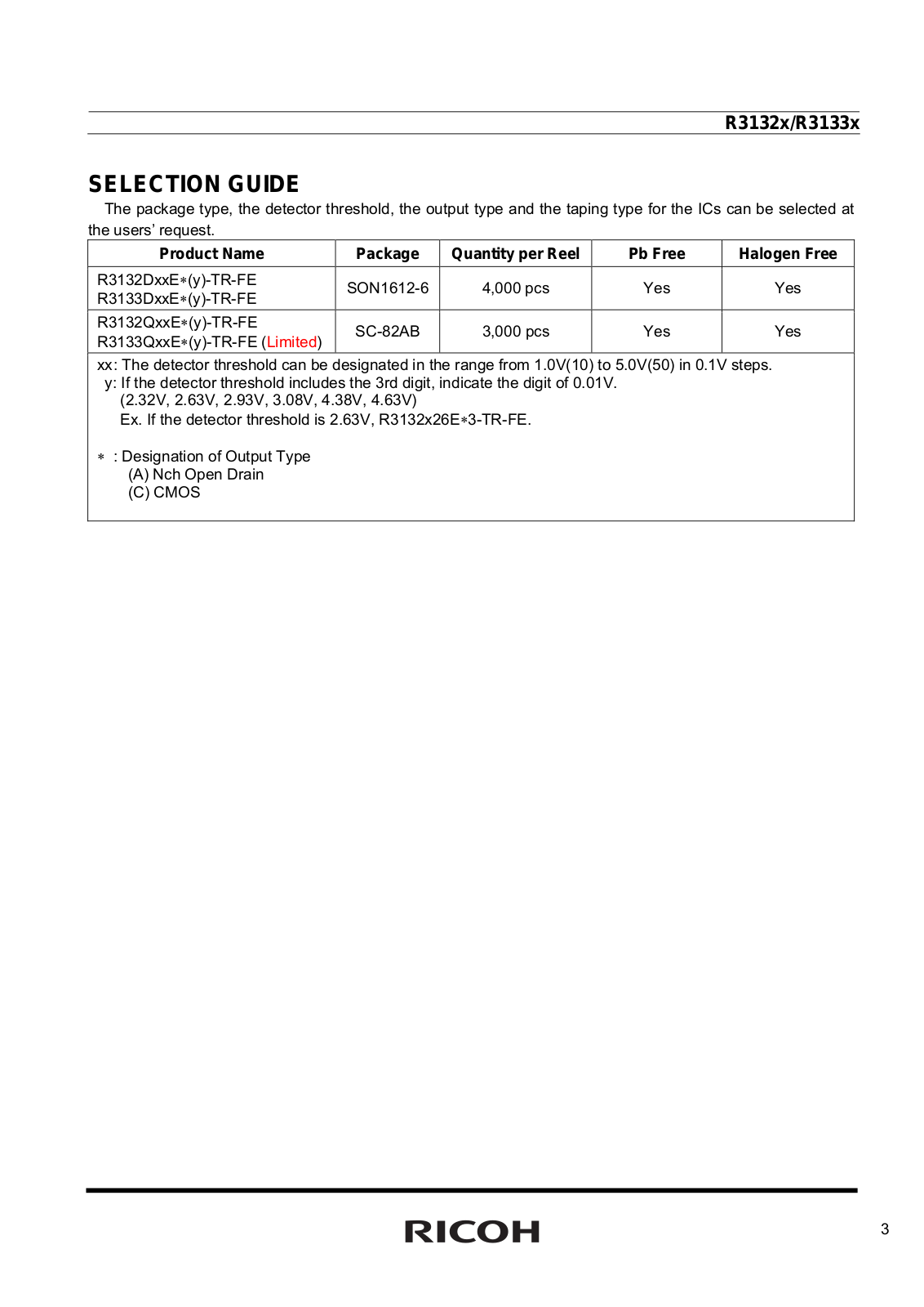
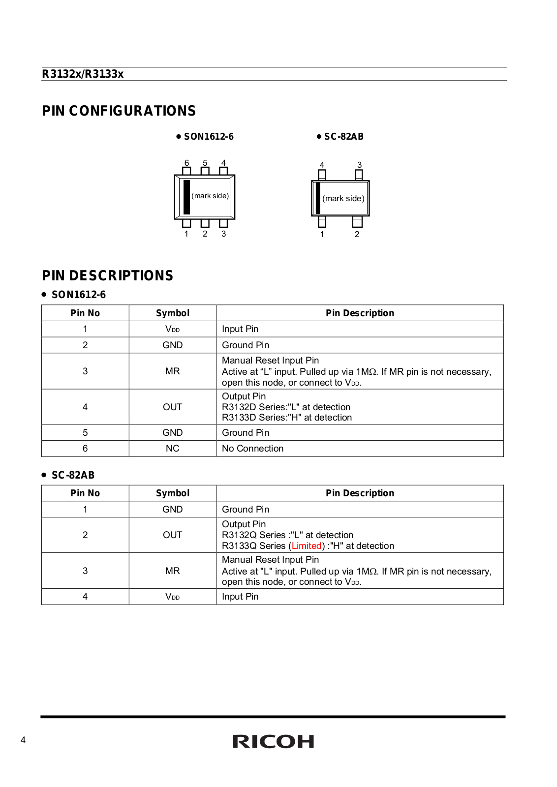
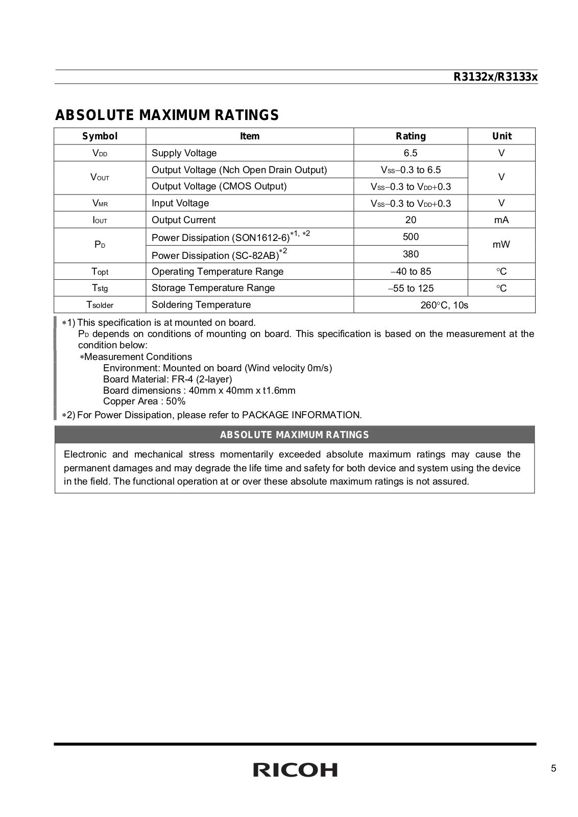
R3132x
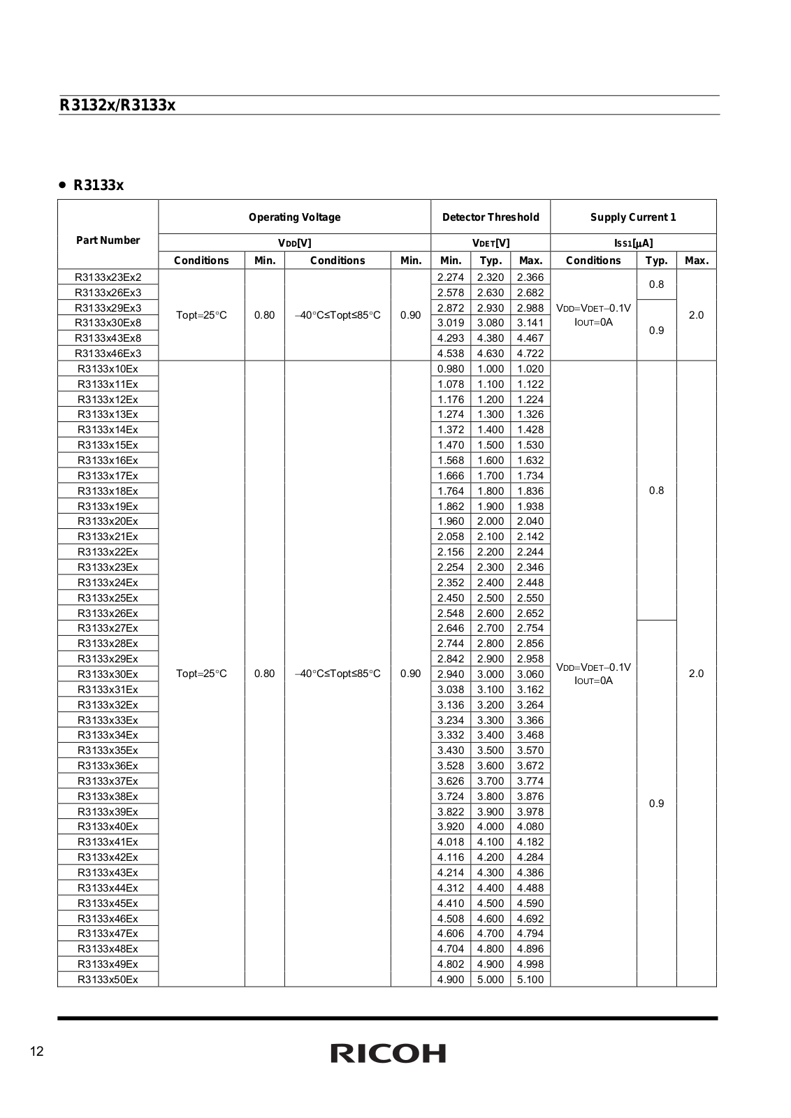
R3133x
R3134x
R314A
R3150N
R316
R316-02
R316A
R317
R318A
R319A
R3200x
2
R320A
R321A
R322A
R3234-01
R3235-01
R323A
R324A
R325A
R325CH02
R325CH14
R326A
R327A
R328A
R329-02
R3292
R329A
R330A
R331
R3310-02
R331-05
R331A
R331B
R332A
R3330-02
R333A
R334A
R335A
R335B
R336A
R3370ZC10#
R3370ZC12#
R337A
R338A
R339A
R3.3L09
R3.3L12
R3.3L15
R3.3M05
R3.3M09
R3.3M12
R3.3M15
R3.3M3.3
R340A
R34100
R34120
R34140
R34160
Loading...
Loading...
Nothing found
R3133x
Datasheet (RICOH)
28 pgs
404.01 Kb
0
Table of contents
Loading...
Datasheet R3132x, R3133x Datasheet (RICOH)
...
Datasheet Datasheet (RICOH)
Download
Specifications and Main Features
Frequently Asked Questions
User Manual
Download
Page 1
Page 2
Page 3
Page 4
Page 5
Page 6
Page 7
Page 8
Page 9
Page 10
Page 11
Page 12
Page 13
Page 14
Page 15
Page 16
Page 17
Page 18
Page 19
Page 20
Page 21
Page 22
Page 23
Page 24
Page 25
Page 26
Page 27
Page 28
Loading...
+
hidden pages
Unhide
You need points to download manuals.
1 point = 1 manual.
You can buy points or you can get point for every manual you upload.
Buy points
Upload your manuals


")