

Page 1

R3111x SERIES
LOW VOLTAGE DETECTOR
NO.EA-056-080131
OUTLINE
The R3111x series are CMOS-based voltage detector ICs with high detector threshold accuracy and ultra-low
supply current, which can be operated at an extremely low voltage and is used for system reset as an example.
Each of these ICs consists of a voltage reference unit, a comparator, resistors for detector threshold setting,
an output driver and a hysteresis circuit. The detector threshold is fixed with high accuracy internally and does
not require any adjustment.
Three output types, Nch open drain “L” type, Nch open drain “H” type and CMOS type are available.
The R3111x Series are operable at a lower voltage than that for the Rx5VL series, and can be driven by a
single battery.
Six types of packages, TO-92, SOT-89, SOT-23-3, SOT-23-5, SC-82AB, and SON1612-6 are available.
FEATURES
• Supply Current......................................................................Typ. 0.8µA (−VDET=1.5V, VDD=−VDET−0.1V)
• Range of Operating Voltage Range......................................0.7V to 10.0V (T
• Detector Threshold Range....................................................0.9V to 6.0V
• Accuracy Detector Threshold................................................±2.0%
• Temperature-Drift Coefficient of Detector Threshold............Typ. ±100ppm/°C
• Output Types.........................................................................Nch Open Drain “L”, Nch Open Drain “H”, and
CMOS
• Packages ..............................................................................TO-92, SOT-89, SOT-23-3, SOT-23-5,
SC-82AB, SON1612-6
opt=25°C)
APPLICATIONS
• CPU and Logic Circuit Reset
• Battery Checker
• Window Comparator
• Wave Shaping Circuit
• Battery Back-up Circuit
• Power Failure Detector
1
Page 2
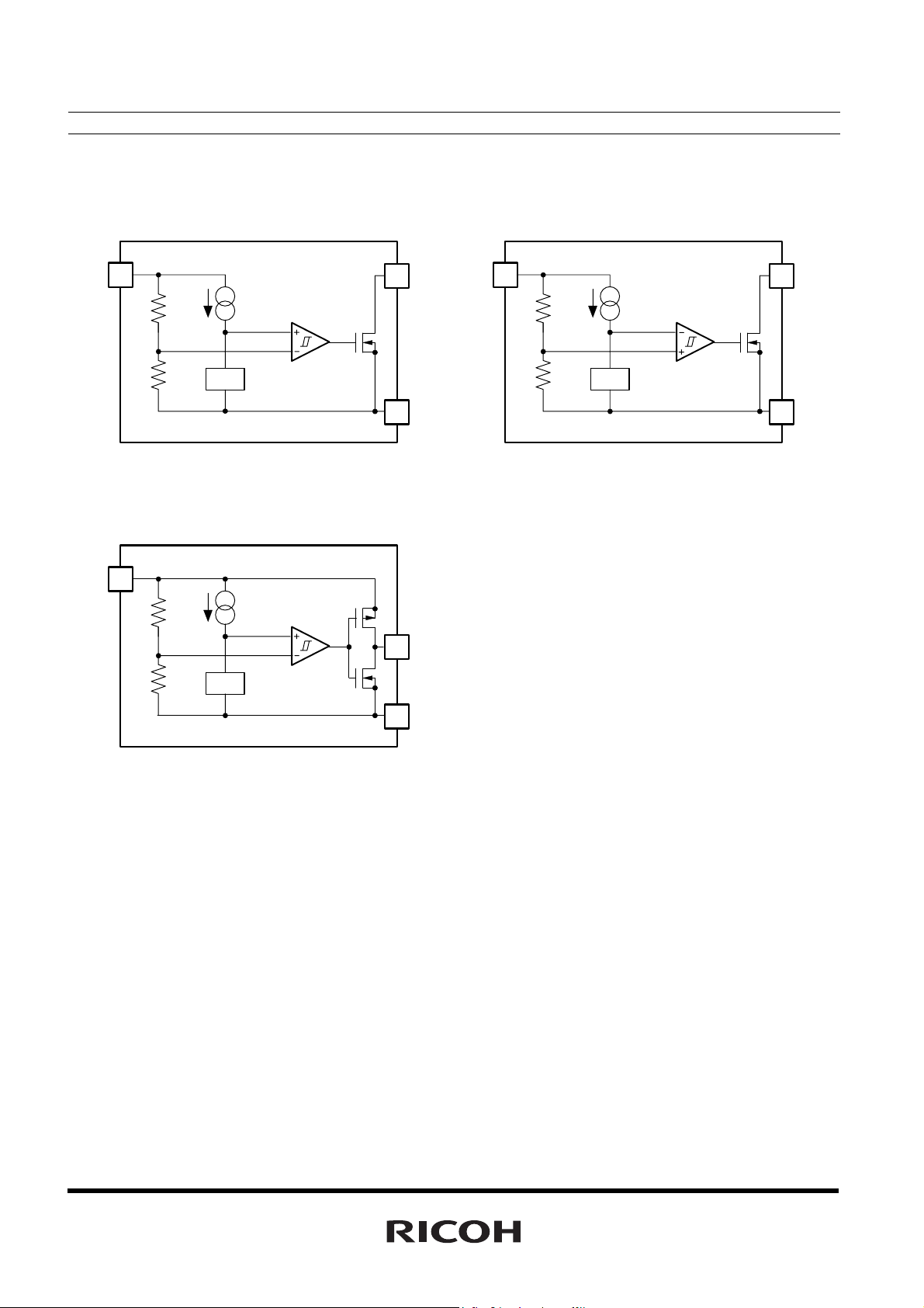
R3111x
BLOCK DIAGRAMS
R3111xxxxA R3111xxxxB
DD
V
OUT
Vref
DD
V
Vref
GND
R3111xxxxC
DD
V
OUT
Vref
GND
OUT
GND
2
Page 3

R3111x
SELECTION GUIDE
The package type, the detector threshold, the output type and the taping type for the ICs can be selected at
the users’ request. The selection can be made with designating the part number as shown below;
R3111xxxxx-xx-x ← Part Number
↑ ↑ ↑ ↑ ↑ ↑
a b c d e f
Code Contents
Designation of Package Type;
D: SON1612-6
a
E: TO-92
H: SOT-89
N: SOT-23-5, SOT-23-3
Q: SC-82AB
b
Setting Detector Threshold (−V
Stepwise setting with a step of 0.1V in the range of 0.9V to 6.0V is possible.
DET);
Designation of Package Type
c
1: except SOT-23-3
2: SOT-23-3
Designation of Output Type;
d
A: Nch Open Drain (Output "L" at V
B: Nch Open Drain (Output "H" at V
C: CMOS (Output "L" at V
DD=−VDET)
DD=−VDET)
DD=−VDET)
Designation of Packing or Taping Type ;
e
Ex.TO-92: TZ, SOT-89: T1, SOT-23-3, SOT-23-5, SC-82AB, SON1612-6: TR
prescribed as standard directions.
(Refer to Taping Specifications.) Antistatic bag for TO-92: C
Designation of Composition of pin plating
f
-F: Lead free solder plating
(TO-92, SOT-89, SOT-23-3, SOT-23-5, SC-82AB, SON1612-6)
3
Page 4
R3111x
PIN CONFIGURATIONS
TO-92 SOT-89 SOT-23-3 SOT-23-5 SC-82AB SON1612-6
3
5
4
43
6 5 4
(mark side)
(mark side)
12
3
(mark side)
1 2
(mark side)
123
(mark side)
1
12
3
PIN DESCRIPTIONS
TO-92 SOT-89 SOT-23-3
Pin No. Symbol
1 VDD
2 GND 2 VDD 2 GND
3 OUT 3 GND 3 VDD
SOT-23-5 SC-82AB SON1612-6
Pin No. Symbol
1 OUT 1 OUT 1 OUT
Pin No. Symbol Pin No. Symbol
1 OUT 1 OUT
Pin No. Symbol Pin No. Symbol
(mark side)
2
1 2 3
2 VDD 2 VDD 2 VDD
3 GND 3 NC 3 GND
4 NC 4 GND 4 NC
5 NC 5 VDD
6 NC
4
Page 5
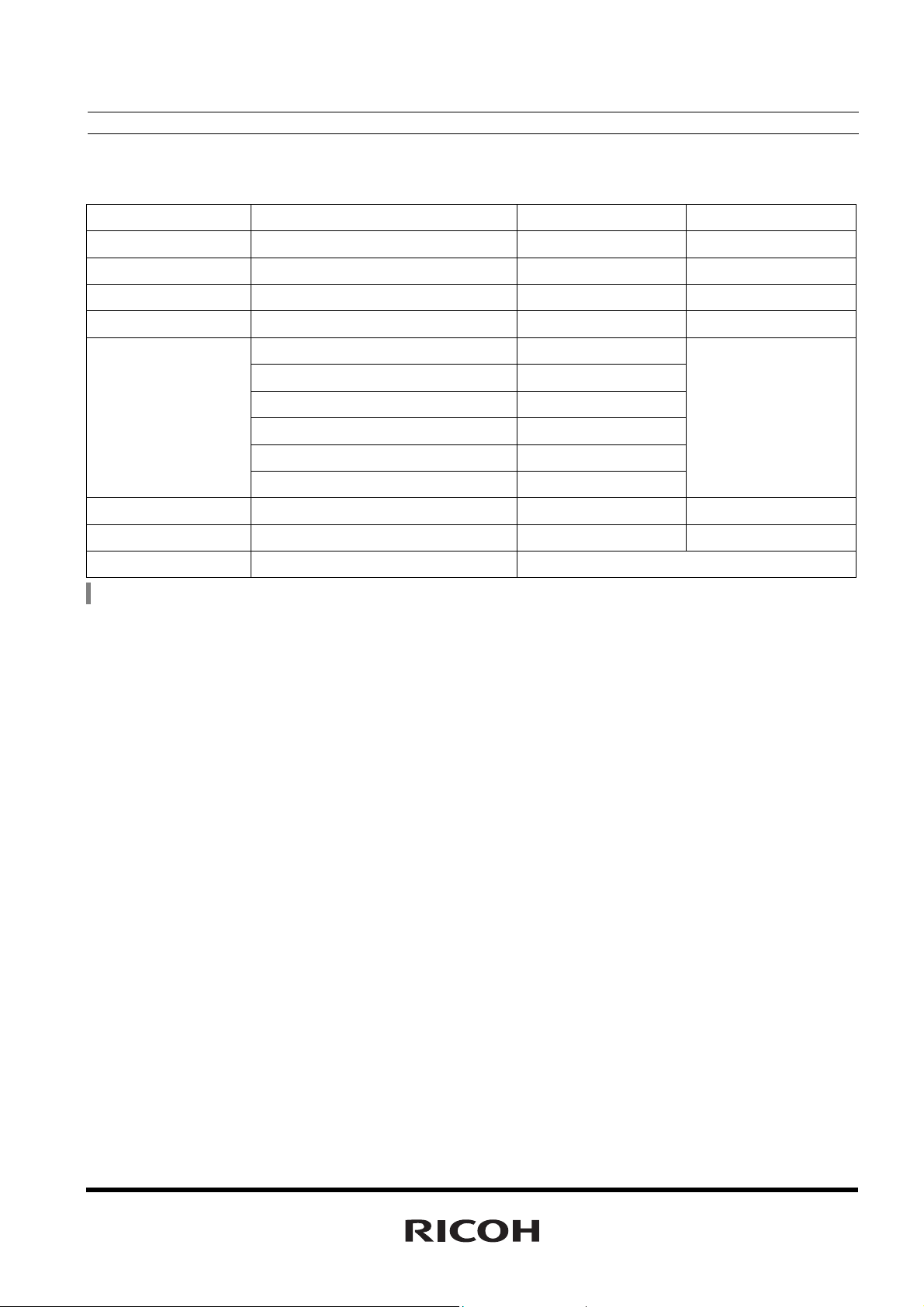
ABSOLUTE MAXIMUM RATINGS
Symbol Item Rating Unit
VDD Supply Voltage 12 V
R3111x
VOUT1 Output Voltage (CMOS)
VOUT2 Output Voltage (Nch)
V
SS−0.3 to VDD+0.3
V
SS−0.3 to 12
IOUT Output Current 70 mA
Power Dissipation (TO-92)* 300
Power Dissipation (SOT-89)* 900
PD
Power Dissipation (SOT-23-3)* 420
Power Dissipation (SOT-23-5)* 420
Power Dissipation (SC-82AB)* 380
Power Dissipation (SON1612-6)* 500
Topt Operating Temperature Range
Tstg Storage Temperature Range
Tsolder Lead temperature (Soldering)
For Power Dissipation, please refer to PACKAGE INFORMATION to be described.
* )
−40 to 85 °C
−55 to 125 °C
V
V
mW
260°C, 10s
5
Page 6
R3111x
<
<
<
<
<
<
<
<
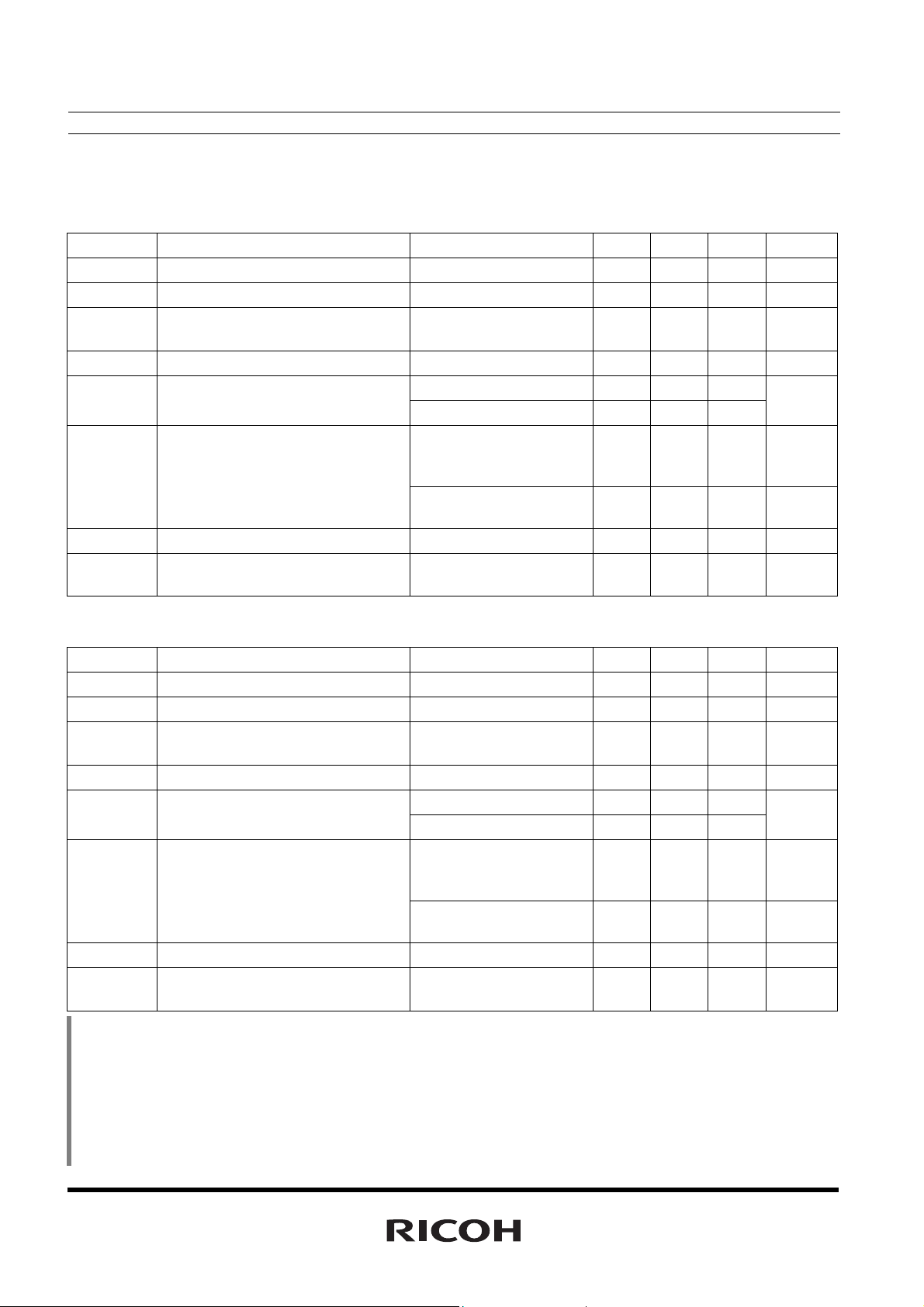
ELECTRICAL CHARACTERISTICS
• R3111x09xA/C Topt=25°C
Symbol Item Conditions Min. Typ. Max. Unit
−VDET
VHYS Detector Threshold Hysteresis 0.027 0.045 0.063 V
ISS Supply Current
VDDH Maximum Operating Voltage 10 V
VDDL
IOUT Output Current (Driver Output Pin)
tPLH
∆−VDET/
∆Topt
• R3111x18xA/C Topt=25°C
Detector Threshold 0.882 0.900 0.918 V
Note1
Minimum Operating Voltage
Note2
Output Delay Time
∗
∗
Detector Threshold Temperature
Coefficient
V
DD=0.80V
DD=2.90V
V
Topt=25°C
−40°C
Topt
Nch
V
DS=0.05V,VDD=0.70V
DS=0.50V,VDD=0.85V
V
Pch
V
DS=−2.1V,VDD=4.5V
85°C
0.55 0.70
0.65 0.80
0.01
0.05
1.0
0.8
0.9
0.05
0.50
2.0
100
−40°C
Topt
85°C
±100
2.4
2.7
µA
V
mA
mA
µs
ppm/°C
Symbol Item Conditions Min. Typ. Max. Unit
−VDET
Detector Threshold 1.764 1.800 1.836 V
VHYS Detector Threshold Hysteresis 0.054 0.090 0.126 V
ISS Supply Current
V
DD=1.70V
DD=3.80V
V
0.8
1.0
2.4
3.0
µA
VDDH Maximum Operating Voltage 10 V
VDDL
Minimum Operating Voltage
IOUT Output Current (Driver Output Pin)
Note2
tPLH
∆−VDET/
∆Topt
∗Note1:
Output Delay Time
Detector Threshold Temperature
Coefficient
Minimum operating voltage means the value of input voltage when output voltage maintains 0.1V or less. (In
∗
the case of Nch Open Drain Output type, the output pin is pulled up with a resistance of 470kΩ to 5.0V.)
Note1
∗
Topt=25°C
−40°C
Topt
85°C
Nch
V
DS=0.05V, VDD=0.70V
DS=0.50V, VDD=1.50V
V
Pch
V
DS=−2.1V,VDD=4.5V
100
−40°C
Topt
85°C
0.55 0.70
0.65 0.80
0.01
1.00
1.0
0.05
2.00
2.0
±100
mA
V
mA
µs
ppm/°C
∗Note2: In the case of CMOS Output type: The time interval between the rising edge of VDD input pulse from 0.7V
to (+VDET)+2.0V and output voltage level becoming to ((+VDET)+2.0V)/2.
In the case of Nch Open Drain Output type: The output pin is pulled up with a resistance of 470kΩ to
5.0V, the time interval between the rising edge of VDD input pulse from 0.7V to (+VDET)+2.0V and output
voltage level becoming to 2.5V.
6
Page 7
R3111x
<
<
<
<
<
<
<
<
• R3111x27xA/C Topt=25°C
Symbol Item Conditions Min. Typ. Max. Unit
−VDET
Detector Threshold 2.646 2.700 2.754 V
VHYS Detector Threshold Hysteresis 0.081 0.135 0.189 V
ISS Supply Current
V
DD=2.60V
DD=4.70V
V
0.9
1.1
2.7
3.3
µA
VDDH Maximum Operating Voltage 10 V
VDDL
Minimum Operating Voltage
IOUT Output Current (Driver Output Pin)
Note2
∗
∆−VDET/
∆Topt
tPLH
Output Delay Time
Detector Threshold Temperature
Coefficient
Note1
∗
Topt=25°C
−40°C
Topt
85°C
Nch
DS=0.05V,VDD=0.70V
V
V
DS=0.50V,VDD=1.50V
Pch
DS=−2.1V,VDD=4.5V
V
100
−40°C
Topt
85°C
0.55 0.70
0.65 0.80
0.01
1.00
1.0
0.05
2.00
2.0
±100
V
mA
mA
µs
ppm/°C
• R3111x36xA/C Topt=25°C
Symbol Item Conditions Min. Typ. Max. Unit
−VDET
Detector Threshold 3.528 3.600 3.672 V
VHYS Detector Threshold Hysteresis 0.108 0.180 0.252 V
ISS Supply Current
V
DD= 3.47V
DD= 5.60V
V
1.0
1.2
3.0
3.6
µA
VDDH Maximum Operating Voltage 10 V
VDDL
Minimum Operating Voltage
IOUT Output Current (Driver Output Pin)
Note2
tPLH
∆−VDET/
∆Topt
∗Note1:
Output Delay Time
Detector Threshold Temperature
Coefficient
Minimum operating voltage means the value of input voltage when output voltage maintains 0.1V or less. (In
∗
the case of Nch Open Drain Output type, the output pin is pulled up with a resistance of 470kΩ to 5.0V.)
Note1
∗
Topt=25°C
−40°C
Topt
85°C
Nch
DS=0.05V,VDD=0.70V
V
V
DS=0.50V,VDD=1.50V
Pch
DS=−2.1V,VDD=4.5V
V
100
−40°C
Topt
85°C
0.55 0.70
0.65 0.80
0.01
1.00
1.0
0.05
2.00
2.0
±100
V
mA
mA
µs
ppm/°C
∗Note2: In the case of CMOS Output type: The time interval between the rising edge of VDD input pulse from 0.7V
to (+VDET)+2.0V and output voltage level becoming to ((+VDET)+2.0V)/2.
In the case of Nch Open Drain Output type: The output pin is pulled up with a resistance of 470kΩ to
5.0V, the time interval between the rising edge of VDD input pulse from 0.7V to (+VDET)+2.0V and output
voltage level becoming to 2.5V.
7
Page 8
R3111x
<
<
<
<
<
<
<
<
• R3111x45xA/C Topt=25°C
Symbol Item Conditions Min. Typ. Max. Unit
−VDET
Detector Threshold 4.410 4.500 4.590 V
VHYS Detector Threshold Hysteresis 0.135 0.225 0.315 V
ISS Supply Current
V
DD=4.34V
DD=6.50V
V
1.1
1.3
3.3
3.9
µA
VDDH Maximum Operating Voltage 10 V
VDDL
Minimum Operating Voltage
∗
IOUT Output Current (Driver Output Pin)
Note2
tPLH
∆−VDET/
∆Topt
Output Delay Time
Detector Threshold Temperature
Coefficient
∗
Note1
Topt=25°C
−40°C
Topt
85°C
Nch
DS=0.05V, VDD=0.70V
V
V
DS=0.50V, VDD=1.50V
Pch
DS=−2.1V,VDD=8.0V
V
100
−40°C
Topt
85°C
0.55 0.70
0.65 0.80
0.01
1.00
1.5
0.05
2.00
3.0
±100
mA
mA
V
µs
ppm/°C
• R3111x54xA/C Topt=25°C
Symbol Item Conditions Min. Typ. Max. Unit
−VDET
Detector Threshold 5.292 5.400 5.508 V
VHYS Detector Threshold Hysteresis 0.162 0.270 0.378 V
ISS Supply Current
V
DD=5.20V
DD=7.40V
V
1.2
1.4
3.6
4.2
µA
VDDH Maximum Operating Voltage 10 V
VDDL
IOUT
tPLH
∆−VDET/
∆Topt
∗Note1:
Minimum Operating Voltage
Note1
∗
Topt=25°C
−40°C
Topt
85°C
Nch
V
Output Current
(Driver Output Pin)
DS=0.05V, VDD=0.70V
DS=0.50V, VDD=1.50V
V
Pch
V
DS=−2.1V, VDD=8.0V
Note2
Output Delay Time
∗
Detector Threshold Temperature
Coefficient
100
−40°C
Topt
85°C
Minimum operating voltage means the value of input voltage when output voltage maintains 0.1V or less. (In
the case of Nch Open Drain Output type, the output pin is pulled up with a resistance of 470kΩ to 5.0V.)
0.55 0.70
0.65 0.80
0.01
1.00
1.5
0.05
2.00
3.0
±100
mA
mA
V
µs
ppm/°C
∗Note2: In the case of CMOS Output type: The time interval between the rising edge of VDD input pulse from 0.7V
to (+VDET)+2.0V and output voltage level becoming to ((+VDET)+2.0V)/2.
In the case of Nch Open Drain Output type: The output pin is pulled up with a resistance of 470kΩ to
5.0V, the time interval between the rising edge of VDD input pulse from 0.7V to (+VDET)+2.0V and output
voltage level becoming to 2.5V.
8
Page 9
R3111x
<
<
<
<
<
<
<
<
• R3111Q231B Topt=25°C
Symbol Item Conditions Min. Typ. Max. Unit
−VDET
Detector Threshold 2.254 2.300 2.346 V
VHYS Detector Threshold Hysteresis 0.069 0.115 0.161 V
ISS Supply Current
V
DD=2.2V
DD=4.3V
V
0.9
1.1
2.7
3.3
µA
VDDH Maximum Operating Voltage 10 V
VDDL
Minimum Operating Voltage
∗
IOUT Output Current (Driver Output Pin)
Note2
tPLH
∆−VDET/
∆Topt
Output Delay Time
Detector Threshold Temperature
Coefficient
∗
Note1
Topt=25°C
−40°C
Topt
85°C
Nch
DS=0.50V,VDD=3.0V
V
100
−40°C
Topt
85°C
0.55 0.70
V
0.65 0.80
2.5 mA
µs
±100
ppm/°C
• R3111Q441B Topt=25°C
Symbol Item Conditions Min. Typ. Max. Unit
−VDET
VHYS Detector Threshold Hysteresis 0.132 0.220 0.308 V
ISS Supply Current
VDDH Maximum Operating Voltage 10 V
VDDL
IOUT
tPLH
∆−VDET/
∆Topt
∗Note1:
∗Note2: In the case of CMOS Output type: The time interval between the rising edge of VDD input pulse from 0.7V
Detector Threshold 4.312 4.400 4.488 V
Note1
Minimum Operating Voltage
∗
Output Current
(Driver Output Pin)
Note2
Output Delay Time
∗
Detector Threshold Temperature
Coefficient
V
DD=4.24V
DD=6.4V
V
Topt=25°C
−40°C
Nch
V
DS=0.50V, VDD=5.5V
Topt
85°C
0.55 0.70
0.65 0.80
2.5 mA
100
−40°C
Topt
85°C
1.1
1.3
±100
3.3
3.9
µA
V
µs
ppm/°C
Minimum operating voltage means the value of input voltage when output voltage maintains 0.1V or less. (In
the case of Nch Open Drain Output type, the output pin is pulled up with a resistance of 470kΩ to 5.0V.)
to (+VDET)+2.0V and output voltage level becoming to ((+VDET)+2.0V)/2.
In the case of Nch Open Drain Output type: The output pin is pulled up with a resistance of 470kΩ to
5.0V, the time interval between the rising edge of VDD input pulse from 0.7V to (+VDET)+2.0V and output
voltage level becoming to 2.5V.
9
Page 10
R3111x
+
+
+
+
TIMING CHART
Supply
Voltage
(VDD)
Minimum Operating Voltage
Released Voltage
Detector Threshold
+V
-
V
V
GND
DET
DET
DDL
Detector Threshold
Hysteresis Hysteresis Hysteresis
Detector Threshold Detector Threshold
Output
Voltage
OUT
(V
)
Pull-up Voltage
GND
t
PLH
t
PLH
t
PLH
R3111xxxxA R3111xxxxB R3111xxxxC
DEFINITION OF OUTPUT DELAY TIME
Output Delay Time (tPLH) is defined as follows:
1. In the case of Nch Open Drain Output:(R3111xxxxA/B)
Under the condition of the output pin (OUT) is pulled up through a resistor of 470kΩ to 5V, the time interval
between the rising edge of V
2. In the case of CMOS Output:(R3111xxxxC)
The time interval between the rising edge of V
voltage to ((+V
DET)+2.0V)/2.
+V
DET
+2.0V
Supply
Voltage
(V
DD
0.7V
)
GND
5.0V
DD pulse from 0.7V to (+VDET)+2.0V and becoming of the output voltage to 2.5V.
DD pulse from 0.7V to (+VDET)+2.0V and becoming of the output
Supply
Voltage
(V
+V
DD
)
DET
2.0V
0.7V
GND
5.0V
Supply
Voltage
DD
(V
V
)
V
DET
+2.0V
DET
+2.0V
0.7V
GND
Output
Voltage
OUT
(V
)
2.5V
GND
PHL
t
PLH
t
Output
Voltage
OUT
(V
2.5V
)
GND
t
PHL
t
PLH
Output
Voltage
(V
OUT
DET
V
)
+2.0V
2
GND
t
PHL
t
PLH
Nch Open Drain Output Nch Open Drain Output CMOS Output
(R3111xxxxA) (R3111xxxxB) (R3111xxxxC)
10
Page 11

R3111x
11
Page 12
R3111x
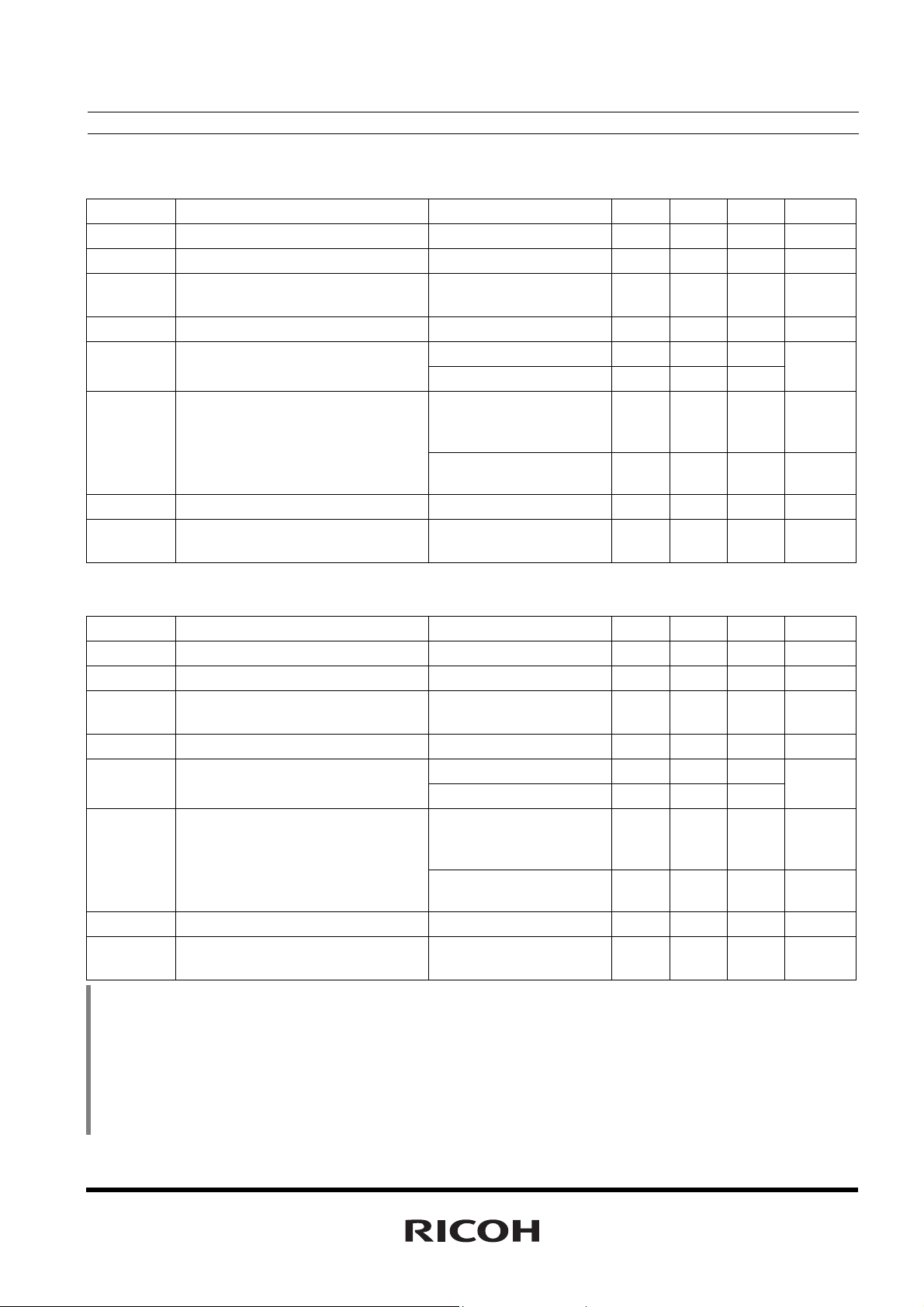
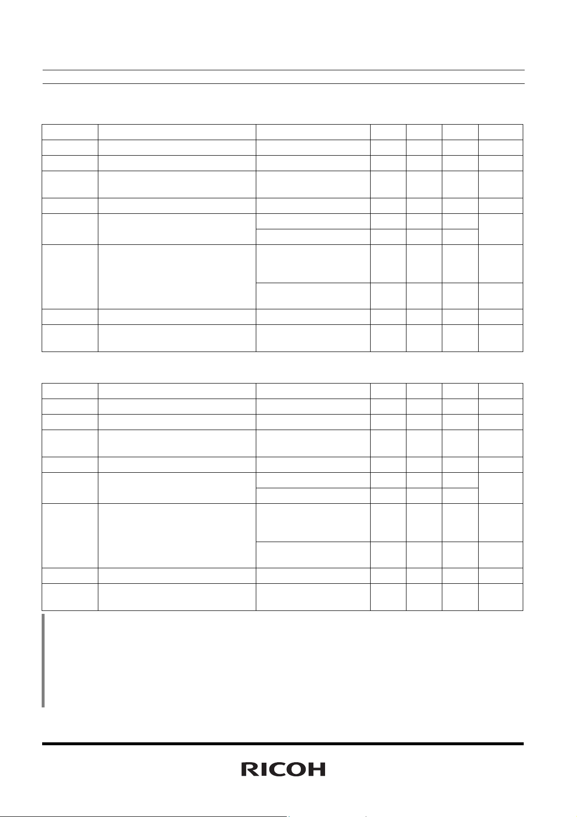
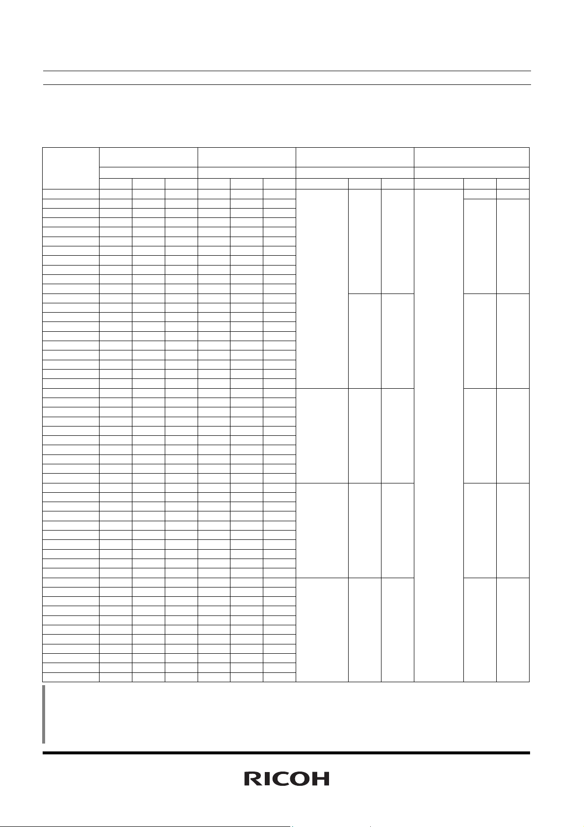
ELECTRICAL CHARACTERISTICS BY DETECTOR THRESHOLD
• R3111x09x to R3111x60x
Part
Number
R3111x09xx 0.882 0.900 0.918 0.027 0.045 0.063 0.9 2.7
R3111x10xx 0.980 1.000 1.020 0.030 0.050 0.070
R3111x11xx 1.078 1.100 1.122 0.033 0.055 0.077
R3111x12xx 1.176 1.200 1.224 0.036 0.060 0.084
R3111x13xx 1.274 1.300 1.326 0.039 0.065 0.091
R3111x14xx 1.372 1.400 1.428 0.042 0.070 0.098
R3111x15xx 1.470 1.500 1.530 0.045 0.075 0.105
R3111x16xx 1.568 1.600 1.632 0.048 0.080 0.112
R3111x17xx 1.666 1.700 1.734 0.051 0.085 0.119
R3111x18xx 1.764 1.800 1.836 0.054 0.090 0.126
R3111x19xx 1.862 1.900 1.938 0.057 0.095 0.133
R3111x20xx 1.960 2.000 2.040 0.060 0.100 0.140
R3111x21xx 2.058 2.100 2.142 0.063 0.105 0.147
R3111x22xx 2.156 2.200 2.244 0.066 0.110 0.154
R3111x23xx 2.254 2.300 2.346 0.069 0.115 0.161
R3111x24xx 2.352 2.400 2.448 0.072 0.120 0.168
R3111x25xx 2.450 2.500 2.550 0.075 0.125 0.175
R3111x26xx 2.548 2.600 2.652 0.078 0.130 0.182
R3111x27xx 2.646 2.700 2.754 0.081 0.135 0.189
R3111x28xx 2.744 2.800 2.856 0.084 0.140 0.196
R3111x29xx 2.842 2.900 2.958 0.087 0.145 0.203
R3111x30xx 2.940 3.000 3.060 0.090 0.150 0.210
R3111x31xx 3.038 3.100 3.162 0.093 0.155 0.217
R3111x32xx 3.136 3.200 3.264 0.096 0.160 0.224
R3111x33xx 3.234 3.300 3.366 0.099 0.165 0.231
R3111x34xx 3.332 3.400 3.468 0.102 0.170 0.238
R3111x35xx 3.430 3.500 3.570 0.105 0.175 0.245
R3111x36xx 3.528 3.600 3.672 0.108 0.180 0.252
R3111x37xx 3.626 3.700 3.774 0.111 0.185 0.259
R3111x38xx 3.724 3.800 3.876 0.114 0.190 0.266
R3111x39xx 3.822 3.900 3.978 0.117 0.195 0.273
R3111x40xx 3.920 4.000 4.080 0.120 0.200 0.280
R3111x41xx 4.018 4.100 4.182 0.123 0.205 0.287
R3111x42xx 4.116 4.200 4.284 0.126 0.210 0.294
R3111x43xx 4.214 4.300 4.386 0.129 0.215 0.301
R3111x44xx 4.312 4.400 4.488 0.132 0.220 0.308
R3111x45xx 4.410 4.500 4.590 0.135 0.225 0.315
R3111x46xx 4.508 4.600 4.692 0.138 0.230 0.322
R3111x47xx 4.606 4.700 4.794 0.141 0.235 0.329
R3111x48xx 4.704 4.800 4.896 0.144 0.240 0.336
R3111x49xx 4.802 4.900 4.998 0.147 0.245 0.343
R3111x50xx 4.900 5.000 5.100 0.150 0.250 0.350
R3111x51xx 4.998 5.100 5.202 0.153 0.255 0.357
R3111x52xx 5.096 5.200 5.304 0.156 0.260 0.364
R3111x53xx 5.194 5.300 5.406 0.159 0.265 0.371
R3111x54xx 5.292 5.400 5.508 0.162 0.270 0.378
R3111x55xx 5.390 5.500 5.610 0.165 0.275 0.385
R3111x56xx 5.488 5.600 5.712 0.168 0.280 0.392
R3111x57xx 5.586 5.700 5.814 0.171 0.285 0.399
R3111x58xx 5.684 5.800 5.916 0.174 0.290 0.406
R3111x59xx 5.782 5.900 6.018 0.177 0.295 0.413
R3111x60xx 5.880 6.000 6.120 0.180 0.300 0.420
*1)
In the case of CMOS output ty pe; when the voltage is forced to VDD from 0.7V to (+V
((+V
DET
(+V
DET
*2) VDD value when Output Voltage is equal or less than 0.1V. In the case of Nch open drain output type, the output pin is pulled up to 5V through 470kΩ
)+2.0V, time interval between the rising edge of VDD and the reaching point at ((+V
resistor.
Condition 1: Topt=25°C
Condition 2: −40°C
Detector Threshold
[V]
<
=
85°C
−VDET
Min. Typ. Max. Min. Typ. Max. Condition Typ. Max. Condition Typ. Max.
)+2.0V)/2. In the case of Nch open drain output type : The output pin is pulled up to 5V through 470kΩ, and when the voltage is forced to VDD from 0.7V to
<
Topt
=
Detector Threshold
Hysteresis
[V]
HYS
V
Supply Current 1 Supply Current 2
V
DD=
(
−VDET)
[µA]
I
I
SS1
0.8 2.4
[µA]
SS2
1.0 3.0
−0.10V
0.9 2.7 1.1 3.3
V
DD=
(
−VDET)
−0.13V
DD=
V
(
−VDET)
1.0 3.0 1.2 3.6
1.1 3.3 1.3 3.9
DD=
V
(
−VDET)
+2.0V
−0.16V
V
DD=
(
−VDET)
1.2 3.6
1.4 4.2
−0.20V
DET
)+2.0V, time interval between the rising ed ge of VDD and the reaching point at
DET
)+2.0V)/2.
12
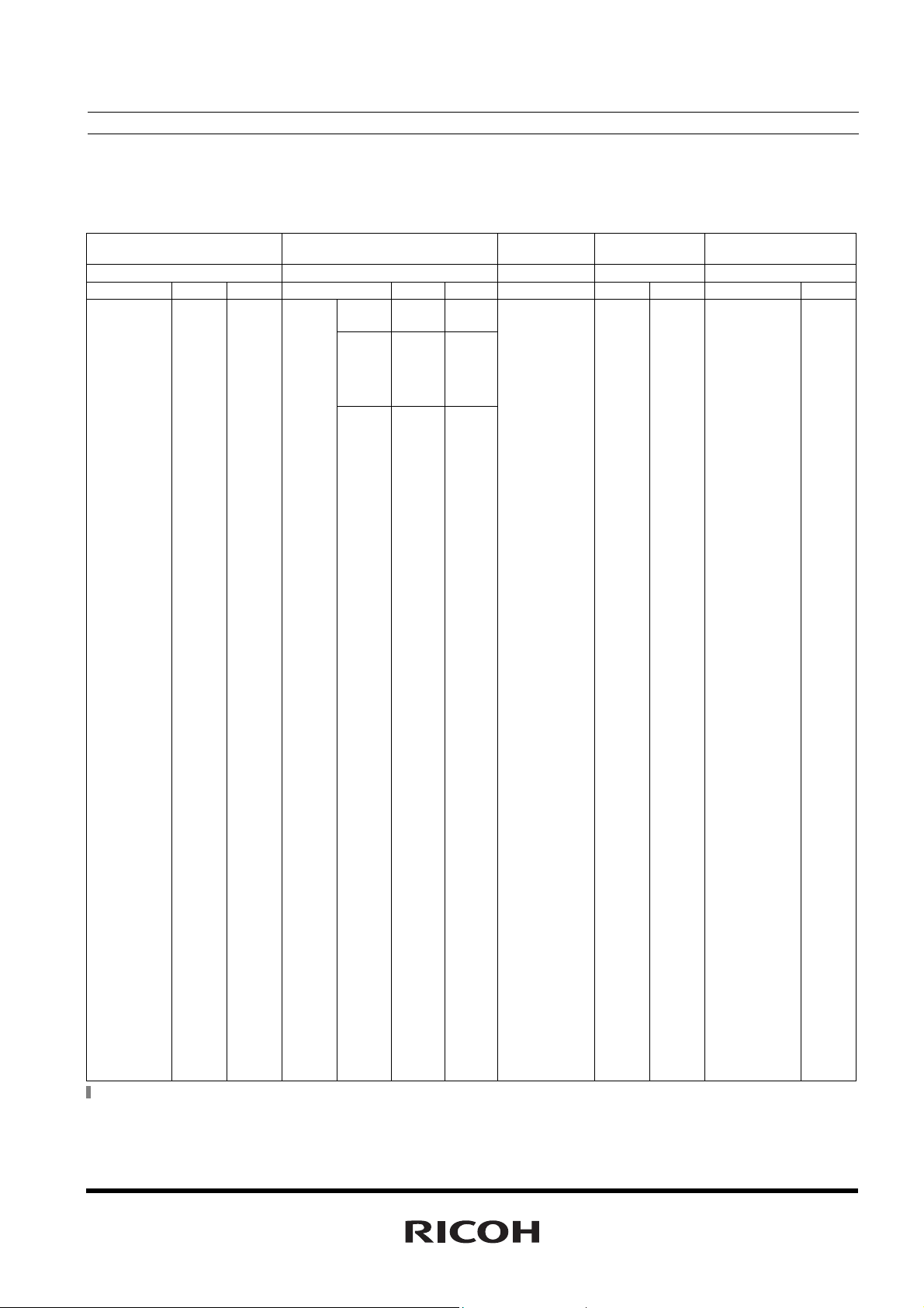
Page 13
R3111x
<
Output Current 1 *3 Output Current 2 *3
[mA]
IOUT1
Condition Min. Typ. Condition Min. Typ. Max. Typ. Max. Condition Typ.
I
OUT2
VDD=
0.85V
[mA]
0.05 0.5
Output Delay
Time
[µs]
t
PLH
Minimum
Operating Voltage
[V]
DDL
V
Detector Threshold
Temperature Coefficient
∆−V
DET/∆Topt
[
ppm/°C
]
Nch
V
DS=0.05V
V
DD=0.7V
0.01 0.05
Nch
V
DS=
0.5V
VDD=
1.0V
DD=
V
1.5V
0.2 1.0
1.0 2.0
100
*2
Condition 1
1
*
0.55
Condition 2
0.65
2
*
Condition 1
0.70
Condition 2
0.80
−40°C
Topt
<
=
±100
85°C
*3) Output Current (IOUT) of R3111xxxxB has not been described. Please inquire details.
13
Page 14
R3111x
p
A
OPERATION
• Operation of R3111xxxxA
Com
Ra
Rb
Vref
Rc
Released Voltage
Detector Threshold
Supply Voltage
DD
(V
)
Minimum Operating Voltage
Pull-up Voltage
Output Voltage
OUT
(V
)
+V
-
GND
GND
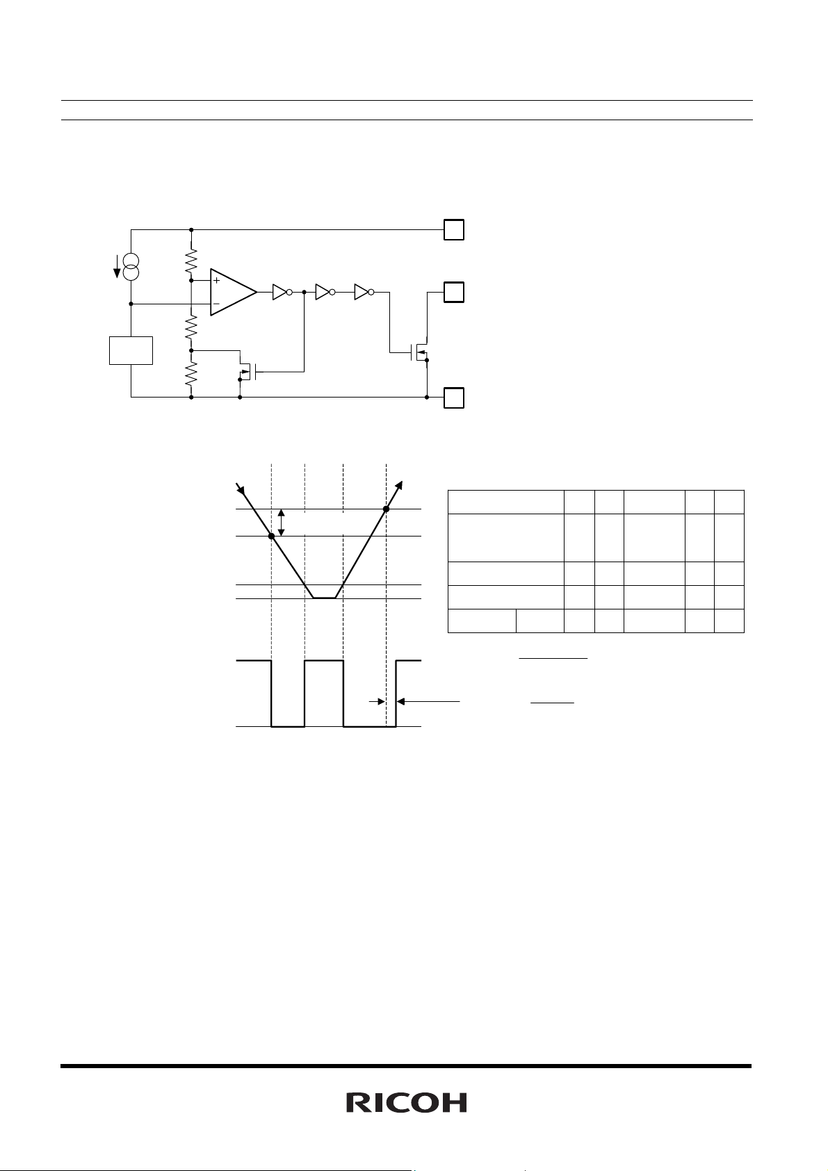
• Explanation of operation
arator
13 5
DET
DET
V
DDL
V
Tr.1
2 4
Detector Threshold
Hysteresis
DD
V
OUT
Nch
GND
Block Diagram (R3111xxxxA)
Step 1 2 3 4 5
B
Comparator (+)
Pin Input Voltage
Comparator Output H L Indefinite L H
Output Tr. Nch OFF ON Indefinite ON OFF
Output
Delay Time
PLH
t
Operation Diagram
OUT pin should be pulled-up to
DD
V
or an external voltage level.
I II II II I
Tr.1 OFF ON Indefinite ON OFF
Rb+Rc
I
Ra+Rb+Rc
II
Rb
Ra+Rb
×V
×V
DD
DD
Step 1. The output voltage is equal to the pull-up voltage.
Step 2. At Point “A”, Vref
>
VDD×(Rb+Rc)/(Ra+Rb+Rc) is true, as a result, the output of comparator is reversed
=
from "H" to "L", therefore the output voltage becomes the GND level. The voltage level of Point A means
a detector threshold voltage (−V
DET).
Step 3. When the supply voltage is lower than the minimum operating voltage, the operation of the output
transistor becomes indefinite. The output voltage is equal to the pull-up voltage.
Step 4. The output Voltage is equal to the GND level.
Step 5. At Point “B”, Vref
<
VDD×Rb/(Ra+Rb) is true, as a result, the output of comparator is reversed from "L" to
=
"H", then the output voltage is equal to the pull-up voltage. The voltage level of Point B means a released
voltage (+V
DET).
∗) The difference between a released volt age and a d etector threshold volt age i s a detector threshold hysteresi s.
14
Page 15

p
A
• Operation of R3111xxxxB
Com
Ra
arator
Rb
Vref
Rc
Released Voltage
Detector Threshold
Supply Voltage
DD
)
(V
Minimum Operating Voltage
Pull-up Voltage
Output Voltage
OUT
)
(V
1 2 3
DET
+V
DET
-
V
DDL
V
GND
GND
• Explanation of operation
Tr.1
Detector Threshold
Hysteresis
DD
V
OUT
Nch
GND
Block Diagram (R3111xxxxB)
B
Output
Delay Time
PLH
t
Operation Diagram
R3111x
OUT pin should be pulled-up to
DD
V
or an external voltage level.
Step 1 2 3
Comparator (−)
Pin Input Voltage
Comparator Output L H L
Tr.1 OFF ON OFF
Output Tr. Nch ON OFF ON
Rb+Rc
I
Ra+Rb+Rc
II
Rb
Ra+Rb
I II I
DD
×V
DD
×V
Step 1. The output voltage is equal to the GND level.
Step 2. At Point “A”, Vref
>
VDD×(Rb+Rc)/(Ra+Rb+Rc) is true, as a result, the output of comparator is reversed
=
from "L" to "H", therefore the output voltage becomes the pull-up voltage. The voltage level of Point A
means a detector threshold voltage (−V
Step 3. At Point “B”, Vref
<
VDD×Rb/(Ra+Rb) is true, as a result, the output of comparator is reversed from "H" to
=
DET).
"L", then the output voltage is equal to the GND level. The voltage level of Point B means a released
voltage (+V
DET).
∗) The difference between a released volt age and a d etector threshold volt age i s a detector threshold hysteresi s.
15
Page 16

R3111x
r
A
• Operation of R3111xxxxC
DD
V
Vref
Released Voltage
Detector Threshold
Supply Voltage
DD
)
(V
Minimum Operating Voltage
Output Voltage
OUT
)
(V
12 3 45
DET
+V
DET
-
V
DDL
V
GND
GND
• Explanation of operation
Ra
Rb
Rc
Detector Threshold
Hysteresis
Comparato
Tr.1
Block Diagram (R3111xxxxC)
B
Output
Delay Time
t
Comparator (+)
Pin Input Voltage
Comparator Output H L Indefinite L H
Output Tr.
PLH
Operation Diagram
Pch
OUT
Nch
GND
Step 1 2 3 4 5
I II II II I
Tr.1 OFF ON Indefinite ON OFF
Pch ON OFF Indefinite OFF ON
Nch OFF ON Indefinite ON OFF
Rb+Rc
I
Ra+Rb+Rc
II
Ra+Rb
Rb
×V
×V
DD
DD
Step 1. The output voltage is equal to the supply voltage (VDD).
Step 2. At Point “A”, Vref
>
VDD×(Rb+Rc)/(Ra+Rb+Rc) is true, as a result, the output of comparator is reversed
=
from "H" to "L", therefore the output voltage becomes the GND level. The voltage level of Point A
means a detector threshold voltage (−V
DET).
Step 3. When the supply voltage is lower than the minimum operating voltage, the operation of the output
transistor becomes indefinite.
Step 4. The output Voltage is equal to the GND level.
Step 5. At Point “B”, Vref
"H", then the output voltage is equal to the supply voltage (V
released voltage (+V
<
VDD×Rb/(Ra+Rb) is true, as a result, the output of comparator is reversed from "L" to
=
DD). The voltage level of Point B means a
DET).
∗) The difference between a released volt age and a d etector threshold volt age i s a detector threshold hysteresi s.
16
Page 17

−
TEST CIRCUITS
SS
I
DD
DD
V
IN
IN
V
R3111x
Series
OUT
V
V
R3111x
Series
OUT
GND
GND
Supply Current Test Circuit Detector Threshold Test Circuit
(Pull-up circuit is not necessary for
CMOS Output type.)
DD
V
OUT
IN
V
R3111x
Series
GND
I
OUT
DS
V
DD
V
V
IN
V
R3111x
Series
OUT
GND
DS
I
470kΩ
OUT
5V
OUT
V
DD
V
V
R3111x
DS
Nch Driver Output Current Test Circuit Pch Driver Output Current Test Circuit
∗Apply to CMOS Output type only
+V
DET
+2.0V
0.7V
GND
P.G.
V
R3111x
Series
GND
DD
OUT
5V
OUT
R
470kΩ
OUT
V
OUT
C
DS
V
DET
+V
+2.0V
0.7V
GND
P.G.
IN
R
470kΩ
DD
V
IN
C
R3111x
Series
GND
OUT
OUT
R
470kΩ
Output Delay Time Test Circuit (1) Output Delay Time Test Circuit (2)
(Pull-up circuit is not necessary for
CMOS Output type.)
5V
V
V
OUT
DS
17
Page 18

R3111x
TYPICAL CHARACTERISTICS
1) Supply Current vs. Input Voltage
R3111x09xC R3111x27xC
2.5
2.0
(µA)
SS
Supply Current I
2.0
1.5
1.0
0.5
0.0
0246810
Input V oltage V
Topt=85°C
IN
(V)
25°C
-40°C
1.5
(µA)
SS
1.0
0.5
Supply Current I
0.0
0246810
Input V oltage V
Topt=85°C
IN
(V)
25°C
-40°C
R3111x45xC
2.0
1.5
(µA)
SS
1.0
0.5
Supply Current I
Topt=85°C
25°C
-40°C
0.0
0246810
IN
Input V oltage V
(V)
2) Detector Threshold Hysteresis vs. Temperature
R3111x09xC R3111x27xC
1.00
0.98
(V)
DET
0.96
0.94
0.92
0.90
0.88
0.86
Detector Threshold -V
0.84
-60 0 20406080-40 -20 100
T emper ature Topt(°C)
+V
-V
DET
DET
2.9
(V)
DET
2.8
2.7
2.6
+V
-V
DET
DET
Detector Threshold -V
2.5
-60 0 20406080-40 -20 100
T emper ature Topt(°C)
18
Page 19

R3111x
R3111x45xC
4.8
(V)
DET
4.7
4.6
+V
DET
4.5
-V
DET
Detector Threshold -V
4.4
-60 0 20406080-40 -20 100
T emper ature Topt(°C)
3) Output Voltage vs. Input Voltage
R3111x09xC R3111x09xA
5V Pull-up 470kΩ
IN(V)
5V Pull-up 470kΩ
IN
(V)
1.6
1.4
(V)
1.2
OUT
1.0
0.8
85°C
0.6
25°C
0.4
Output V oltage V
0.2
Topt=-40°C
0.0
0 0.6 0.8 1 1.2 1.40.2 0.4 1.6
IN
Input V oltage V
(V)
6
5
4
3
2
Output V oltage VOUT(V)
1
0
0 0.6 0.8 1 1.2 1.40.2 0.4 1.6
Topt=-40°C
25°C
85°C
Input V oltage V
R3111x27xC R3111x27xA
4.0
3.5
(V)
3.0
OUT
2.5
2.0
1.5
85°C
1.0
0.5
25°C
Topt=-40°C
Output V oltage V
0.0
0 1.5 2 2.5 3 3.50.5 1 4
Input V oltage V
IN
(V)
6
5
(V)
OUT
4
3
2
Output V oltage V
1
0
Topt=-40°C
25°C
85°C
0 1.5 2 2.5 3 3.50.5 1 4
Input V oltage V
19
Page 20

R3111x
R3111x45xC R3111x45xA
6
5
(V)
OUT
4
3
2
Output V oltage V
1
85°C
25°C
Output V oltage VOUT(V)
6
5
4
3
2
1
Topt=-40°C
25°C
85°C
Topt=-40°C
0
0231654
Input V oltage V
IN
(V)
0
0231654
Input V oltage V
4) Nch Driver Output Current vs. VDS
R3111x09xC R3111x09xC
700
Topt=25°C
300
5V Pull-up 470kΩ
IN(V)
Topt=25°C
600
(µA)
500
OUT
400
300
200
Output Current I
100
0
DD
=0.85V
V
0.7V
0 0.2 0.4 0.6 0.8
V
DS
(V)
250
(µA)
200
OUT
150
100
Output Current I
50
0
0 0.02 0.04 0.06 0.08 0.1
VDD=0.8V
0.7V
V
DS
(V)
R3111x27xC R3111x27xC
20
18
16
14
12
10
8
6
4
Output Current IOUT(mA)
2
0
0 0.5 1 1.5 2 2.5
V
1.5V
DS(V)
Topt=25°C
VDD=2.5V
2.0V
300
250
(µA)
200
OUT
150
100
Output Current I
50
0
0 0.02 0.04 0.06 0.08 0.1
VDD=0.8V
V
DS
(V)
Topt=25°C
0.7V
20
Page 21

R3111x
R3111x45xC R3111x45xC
60
Topt=25°C
300
Topt=25°C
3.0V
VDD=4.5V
4.0V
3.5V
(µA)
OUT
Output Current I
250
200
150
100
50
0
0 0.02 0.04 0.06 0.08 0.1
VDD=0.8V
V
DS
(V)
0.7V
50
40
30
20
10
Output Current IOUT(mA)
0
0 0.5 1 1.5 2 2.5 3 43.5 4.5
1.5V
2.0V
V
DS(V)
2.5V
5) Nch Driver Output Current vs. Input Voltage
R3111x09xC R3111x27xC
900
800
700
(µA)
600
OUT
500
400
300
200
Output Current I
100
0
0 0.2 0.4 0.6 10.8
Input V oltage V
Topt=-85°C
25°C
IN
-40°C
(V)
R3111x45xC
25
14
12
10
8
6
4
Output Current IOUT(mA)
2
0
0 0.5 1 1.5 1 2.5 3
Topt=-40°C
Input Voltage V
IN(V)
25°C
85°C
20
15
10
5
Output Current IOUT(mA)
0
0123456
Topt=-40°C
25°C
85°C
Input Voltage V
IN(V)
21
Page 22

R3111x
6) Pch Driver Output Current vs. Input Voltage
R3111x09xC R3111x27xC
1.4
Topt=25°C
3.5
Topt=25°C
(mA)
OUT
Output Current I
1.2
1.0
0.8
0.6
0.4
0.2
0.0
02468
Input Voltage V
VDS=0.7V
0.5V
IN
(V)
3.0
(mA)
2.5
OUT
2.0
1.5
1.0
Output Current I
0.5
0.0
012 43657
Input Voltage V
VDS=2.1V
1.5V
1.0V
0.5V
IN
(V)
R3111x45xC
IN(V)
Topt=25°C
1.5V
1.0V
0.5V
4.5
4.0
3.5
3.0
2.5
2.0
1.5
1.0
Output Current IOUT(mA)
0.5
0.0
024 8610
Input Voltage V
VDS=2.1V
7) Output Delay Time vs. Load Capacitance (Topt=25°C)
R3111x09xA R3111x27xA
100
100
22
10
1
0.1
0.01
Output Delay Time tP(ms)
0.001
0.0001 0.010.001 0.1
tPLH
tPHL
Load Capacitance C
OUT
(µF)
10
1
0.1
0.01
Output Delay Time tP(ms)
0.001
0.0001 0.010.001 0.1
tPLH
tPHL
Load Capacitance C
OUT
(µF)
Page 23

R3111x
R3111x45xA
100
10
t
1
0.1
0.01
Output Delay Time tP(ms)
0.001
0.0001 0.010.001 0.1
8) Output Delay Time vs. Input Pin Capacitance
R3111x09xA R3111x27xA
100
PLH
t
PHL
Load Capacitance C
OUT
(µF)
100
10
1
0.1
0.01
Output Delay Time tP(ms)
0.001
0.0001 0.010.001 0.1
t
PLH
t
PHL
Input Pin Capacitance C
IN
(µF)
10
t
1
0.1
0.01
Output Delay Time tP(ms)
0.001
0.0001 0.010.001 0.1
Input Pin Capacitance C
PHL
t
PLH
IN
(µF)
R3111x45xA
100
10
1
0.1
0.01
t
PLH
t
PHL
Output Delay Time tP(ms)
0.001
0.001 0.10.01 1
IN
Input Pin Capacitance C
(µF)
23
Page 24

R3111x
k
k
Ω
•
•
k
Ω
A
TYPICAL APPLICATION
• R3111xxxxA CPU Reset Circuit (Nch Open Drain Output)
Case 1. Input Voltage to R3111xxxxA is equal to
Input Voltage to CPU
DD
V
R3111xxxxA
Series
DD
470
R
Ω
DD
V
CPU
RESET
OUT
GND
V
GND
• R3111xxxxC CPU Reset Circuit (CMOS Output)
Case 2. Input Voltage to R3111xxxxA is unequal to
Input Voltage to CPU
DD
V
R3111xxxxA
GND
DD
V
Series
470
OUT
R
DD
V
RESET
GND
CPU
DD2
V
DD
V
R3111xxxxC
Series
DD
V
CPU
RESET
OUT
GND
DD
V
GND
R3111xxxxA Output Delay Time Circuit 1
(Nch Open Drain Output)
DD
V
R3111xxxxA
Series
GND
470
Ω
OUT
R
DD
V
CPU
RESET
GND
DD
V
• Memory Back-up Circuit
DD
V
D1
V
DD
D2
V
B
C
GND
Y1
Y2
Y3
Y4
CC
R3111xxxxA Output Delay Time Circuit 2
(Nch Open Drain Output)
DD
V
DD
V
100k
R1
DD
V
470kΩ
R3111xxxxA
Series
GND
R2
OUT
CC
V
RAM1
GNDCS
CC
V
RAM2
GND CS
CC
V
RAM3
GND CS
CC
V
RAM4
GND CS
CPU
RESET
GND
R3111xxxxC
Series
GND
OUT
24
Page 25

• Voltage level Indicator Circuit (lighted when the power runs out)
(Nch Open Drain Output)
DD
V
DD
V
R3111xxxxA
Series
OUT
GND
• Detector Threshold Adjustable Circuit
(Nch Open Drain Output)
OUT
R3111xxxxA
DD
V
Ra
DD
V
Series
+
C
Rb
GND
Adjusted Detector Threshold
=(−VDET)×(Ra+Rb)/Rb
Hysteresis Voltage
=(VHYS)×(Ra+Rb)/Rb
∗) If the value of Ra is set excessively large, voltage
drop may occur caused by the supply current of IC
itself, and detector threshold may vary.
• Window Comparator Circuit
(Nch Open Drain Output)
DD
V
R3111xxxxA
Series
GND
OUT
DET
V
−
R3111xxxxA
GND
1
DD
V
Series
V
−
OUT
DET
2
DD
V
WC_OUT
DD
V
GND
WC_OUT
−V
DET
R3111x
1
DET
2
−V
• Over-charge Preventing Circuit
Light
R1
Solar Battery
R3
D1
OUT
DD
V
R3111xxxxC
Series
GND
GND
R4R2
Load
25
Page 26

R3111x
TECHNICAL NOTES
When R3111xxxxA/B (Nch Open Drain Output Type) is used in Figure A or Figure B, if impedance of Voltage
Supply pin, V
the consumption current of the IC itself. Released voltage may also shift and delay time for start-up might be
generated by this usage.
When R3111xxxxC (CMOS Output Type) is used in Figure A or Figure B, Output level could be unstable by
cross conduction current which is generated at detector threshold level or at rele ased volt age level, therefore, do
not use this IC with the connection in Figure A or Figure B.
The connection in Figure C may cause the oscillation in both R3111xxxxC (CMOS Output) and R3111xxxxA/B
(Nch Open Drain Output), therefore do not use R3111x Series with the connection in Figure C.
DD and VDD of this IC is large, detector threshold level would shift by voltage dropdown caused by
DD
V
R1
R3111x
Series
OUT
R2
GND GND
DD
V
DD
V
R3111x
Series
GND
R1
OUT
DD
V
DD
V
R3111x
Series
R1
Figure A Figure B Figure C
OUT
R2
26
Page 27

PACKAGE INFORMATION
PE-TO-92-0611
• TO-92 (SC-43A) Unit: mm
PACKAGE DIMENSIONS
5.2Max.
4.2Max.
5.2 Max.
4.2 Max.
5.2Max.12.7Min.
2.3Max.
0.6Max.
0.55Max.
1
0.7
3
2
1.27
2.54
TAPING SPECIFICATION
±1.0
12.7
0.5 Max.
6.0±0.5
9.0±0.5
–0.5
+1.0
18.0
0.3
±
12.7
0.5Max.
5.2 Max.12.7 Min.
2.3 Max.
0.6 Max.
0.7
0.55
Max.
+0.4
2.5
–0.1
2
1
3
*
16.0±0.5
19.0±0.5
24.7 Max.
1.45 Max.
0.7±0.2
φ4.0±0.2
(Note) When taping is performed,the pins of TO-92 are
subjected to a particular forming.
0.5 Max.
: Mark Side
(Note) TZ type tape is not in the form of a reel,but is
packed in a zigzag state in box.Therefore,the
tape can be used as either an RF type tape or
an RR type tape,depending upon the pulling out
direction (B or F).
PACKING BOX DIMENSIONS (TZ)
When TZ type tape is
pulled out from the
direction B
When TZ type tape is
pulled out from the
direction F
User Direction of Feed
TAPING REEL DIMENSIONS
RF RR
*
(Note)
(RF, RR)
(1reel=2000pcs) (1box=2500pcs)
53
43
∅30
∅80
∅360
47
F
265 or 200
B
335
Page 28

PACKAGE INFORMATION
POWER DISSIPATION (TO-92)
This specification is at mounted on board.
Measurement Result (Topt=25°C,Tjmax=125°C)
Free Air
Power Dissipation 300mW
Thermal Resistance
500
400
300
200
100
Power Dissipation PD(mW)
θja=(125−25°C)/0.3W=333°C/W
Free Air
PE-TO-92-0611
0
0 50 10025 75 85 125 150
Ambient Temperature (°C)
Power Dissipation
Page 29

PACKAGE INFORMATION
PE-SOT-89-071210
• SOT-89 (SC-62) Unit: mm
PACKAGE DIMENSIONS
4.5±0.1
1.6±0.2
∅1.0
12
+0.25
−0.35
2.5±0.11.0±0.2
4.0
3
1.5±0.1
0.4±0.1
0.4±0.1
0.1 S
1
3
2
0.3±0.2
S
0.47
0.42±0.1
1.5±0.1
±0.1
1.5±0.1
0.42±0.1
TAPING SPECIFICATION (T1: Standard Type)
+0.1
1.5
2.5Max.
0.3±0.1
∅
5.0
T1
User Direction of Feed
0
8.0±0.1
4.0±0.1
2.0±0.05
4.7
∅1.6±0.1
TAPING REEL DIMENSIONS
1.5±0.1
5.65±0.05
12±0.3
Bottom View
(1reel=1000pcs)
2±0.5
21±0.8
15.4±1.0
13±0.3
13±0.2∅
0
−1.5
+1
0
∅ 60
∅ 180
Page 30

PACKAGE INFORMATION
PE-SOT-89-071210
POWER DISSIPATION (SOT-89)
This specification is at mounted on board. Power Dissipation (PD) depends on conditions of mounting on board.
This specification is based on the measurement at the condition below:
Measurement Conditions
Standard Land Pattern
Environment Mounting on Board (Wind velocity=0m/s)
Board Material Glass cloth epoxy plastic (Double sided)
Board Dimensions
Copper Ratio Top side : Approx. 10% , Back side : Approx. 100%
Through-hole -
Measurement Result (Topt=25°C,Tjmax=125°C)
Standard Land Pattern Free Air
Power Dissipation 900mW 500mW
Thermal Resistance
1000
900
θja=(125−25°C)/0.9W=111°C/W 200°C/W
50mm
× 50mm × 1.6mm
50
On Board
750
(mW)
D
Free Air
500
50
250
Power Dissipation P
0
0 50 10025 75 125 150
Ambient Temperature (°C)
Power Dissipation Measurement Board Pattern
IC Mount Area (Unit : mm)
RECOMMENDED LAND PATTERN (SOT-89)
2.0
3.0
45°
0.71.5
1.0
1.0
1.0
1.5
1.5
(Unit : mm)
Page 31

PACKAGE INFORMATION
PE-SOT-23-5-071228
• SOT-23-5 (SC-74A) Unit: mm
PACKAGE DIMENSIONS
2.9±0.2
1.9±0.2
(0.95) (0.95)
54
+0.2
−0.1
1.6
2.8–0.3
1.1
+0.2
−0.1
0.8±0.1
0 to 0.1
123
0.4±0.1
0.15
+0.1
−0.05
0.2 Min.
TAPING SPECIFICATION
4.0–0.1
4.0–0.1
2.0–0.05
∅1.1±0.1
1.75–0.1
3.5–0.05
8.0–0.3
+0.1
φ1.5
0.3–0.1
3.2
3.3
2.0Max.
0
TR
User Direction of Feed
TAPING REEL DIMENSIONS REUSE REEL (EIAJ-RRM-08Bc)
(1reel=3000pcs)
21±0.8
2±0.5
11.4±1.0
9.0±0.3
13±0.2
∅
0
+1
−1.5
0
60
180
∅
∅
Page 32

PACKAGE INFORMATION
PE-SOT-23-5-071228
POWER DISSIPATION (SOT-23-5)
This specification is at mounted on board. Power Dissipation (PD) depends on conditions of mounting on board.
This specification is based on the measurement at the condition below:
(Power Dissipation (SOT-23-5) is substitution of SOT-23-6.)
Measurement Conditions
Standard Land Pattern
Environment Mounting on Board (Wind velocity=0m/s)
Board Material Glass cloth epoxy plastic (Double sided)
Board Dimensions
Copper Ratio Top side : Approx. 50% , Back side : Approx. 50%
Through-hole
Measurement Result (Topt=25°C, Tjmax=125°C)
Standard Land Pattern Free Air
Power Dissipation 420mW 250mW
Thermal Resistance
600
500
420
(mW)
D
400
300
250
On Board
θja=(125−25°C)/0.42W=238°C/W 400°C/W
Free Air
40mm × 40mm × 1.6mm
φ0.5mm × 44pcs
40
200
Power Dissipation P
100
0
0 50 10025 75 85 125 150
Ambient Temperature (°C)
40
Power Dissipation Measurement Board Pattern
IC Mount Area Unit : mm
RECOMMENDED LAND PATTERN
0.7 MAX.
1.0
2.4
0.95
0.95
1.9
(Unit: mm)
Page 33

PACKAGE INFORMATION
PE-SOT-23-3-0510
• SOT-23-3 (SC-59A) Unit: mm
PACKAGE DIMENSIONS
1.4MAX.
2.9±0.2
0.4±0.1
3
1.6±0.2
2.8±0.3
12
(0.95) (0.95)
1.9±0.2
1.1
0.16
+0.2
–0.1
0.8
+0.1
–0.06
0 to 0.1
0.2 MIN.
TAPING SPECIFICATION (T1: Standard Type)
0.3±0.1
2.0MAX.
User Direction of Feed
TAPING REEL DIMENSIONS
(1reel=3000pcs)
21±0.8
TR
2±0.5
4.0±0.1
+0.1
∅
1.5
0
4.0±0.1
2.0±0.05
3.2
3.3
∅1.1±0.1
1.75±0.1
3.5±0.05
8.0±0.3
11.4±1.0
9.0±0.3
13±0.2
0
–1.5
+1
0
60
180
Page 34

PACKAGE INFORMATION
PE-SOT-23-3-0510
POWER DISSIPATION (SOT-23-3)
This specification is at mounted on board. Power Dissipation (PD) depends on conditions of mounting on board.
This specification is based on the measurement at the condition below:
(Power Dissipation (SOT-23-3) is substitution of SOT-23-6.)
Measurement Conditions
Standard Land Pattern
Environment Mounting on Board (Wind velocity=0m/s)
Board Material Glass cloth epoxy plactic (Double sided)
Board Dimensions
Copper Ratio Top side : Approx. 50% , Back side : Approx. 50%
Through-hole
Measurement Result
Standard Land Pattern Free Air
Power Dissipation 420mW 250mW
Thermal Resistance
600
500
420
(mW)
D
400
300
250
θja=(125−25°C)/0.42W=263°C/W 400°C/W
On Board
Free Air
40mm × 40mm × 1.6mm
φ0.5mm × 44pcs
(Topt=25°C,Tjmax=125°C)
40
200
Power Dissipation P
100
0
0 50 10025 75 85 125 150
Ambient Temperature (°C)
40
Power Dissipation Measurement Board Pattern
IC Mount Area Unit : mm
RECOMMENDED LAND PATTERN (SOT-23-3)
0.7 MAX.
1.0
2.4
0.95
0.95
1.9
(Unit: mm)
Page 35

PACKAGE INFORMATION
PE-SC-82AB-0512
• SC-82AB Unit: mm
PACKAGE DIMENSIONS
2±0.2
1.3±0.2
0.3±0.1 0.3±0.1
4
3
±0.2
1.25
−0.1
2.1±0.3
0.9±0.1
(0.7)
0.3±0.2
0 to 0.1
0.3±0.1
TAPING SPECIFICATION
0.2±0.1
1.6MAX.
TAPING REEL DIMENSIONS
21
0.4±0.1
0.05
+0.1
∅
1.5
0
4.0±0.1
TR
User Direction of Feed
4.0±0.1
2.2
0.16
2.0±0.05
2.6
∅1.1±0.1
+0.1
−0.06
1.75±0.1
3.5±0.05
8.0±0.3
(1reel=3000pcs)
21±0.8
2±0.5
11.4±1.0
9.0±0.3
13±0.2
+1
0
−1.5
0
60
180
Page 36

PACKAGE INFORMATION
PE-SC-82AB-0512
POWER DISSIPATION (SC-82AB)
This specification is at mounted on board. Power Dissipation (PD) depends on conditions of mounting on board.
This specification is based on the measurement at the condition below:
Measurement Conditions
Standard Land Pattern
Environment Mounting on Board (Wind velocity=0m/s)
Board Material Glass cloth epoxy plactic (Double sided)
Board Dimensions
Copper Ratio Top side : Approx. 50% , Back side : Approx. 50%
Through-hole
Measurement Result
Standard Land Pattern Free Air
Power Dissipation 380mW 150mW
Thermal Resistance
600
θja=(125−25°C)/0.38W=263°C/W 667°C/W
40mm × 40mm × 1.6mm
φ0.5mm × 44pcs
(Topt=25°C,Tjmax=125°C)
500
(mW)
D
Power Dissipation P
380
400
300
200
150
100
0
0 50 10025 75 85 125 150
On Board
Free Air
Ambient Temperature (°C)
40
40
Power Dissipation Measurement Board Pattern
IC Mount Area (Unit : mm)
RECOMMENDED LAND PATTERN
0.650.65
0.6 0.6
0.8
0.8
1.9
0.8
0.8
0.6
0.65
0.8
0.6
(Unit: mm)
Page 37

PACKAGE INFORMATION
PE-SON1612-6-0510
• SON1612-6 Unit: mm
PACKAGE DIMENSIONS
1.6±0.1
64
1.2±0.05
1.6±0.05
0.3TYP.
(0.2)
0.5
(0.3)(0.3)
13
0.6MAX.
0.08
0.22±0.05
TAPING SPECIFICATION
0.25±0.1
1.1MAX.
User Direction of Feed
TAPING REEL DIMENSIONS
0.125±0.055
0.08 M
1.5
TR
+0.1
0
1.75
4.0±0.1
1.75
4.0±0.1
1.1±0.1
2.0±0.05
1.75±0.1
3.5±0.05
8.0±0.3
(1reel=4000pcs)
21±0.8
2±0.5
11.4±1.0
9.0±0.3
13±0.2
∅
0
+1
−1.5
0
60
180
∅
∅
Page 38

PACKAGE INFORMATION
Power Dissipation (SON1612-6)
This specification is at mounted on board.
Power Dissipation (P
measurement at the condition below:
Measurement Conditions
Standard Land Pattern
Environment Mounting on Board (Wind velocity=0m/s)
Board Material Glass cloth epoxy plactic (Double sided)
Board Dimensions
Copper Ratio Top side : Approx. 50%, Back side : Approx.50%
Through-hole
Measurement Result
Standard Land Pattern
Power Dissipation 500mW
Thermal Resistance
600
D) depends on conditions of mounting on board. This specification is based on the
40mm × 40mm × 1.6mm
φ0.5mm × 24pcs
(Topt=25°C,Tjmax=125°C)
θja=(125−25°C)/0.5W=200°C/W
PE-SON1612-6-0510
39
500
(mW)
D
400
300
200
Power Dissipation P
100
0
0 50 10025 75 85 125 150
Ambient Temperature (°C)
On Board
40
27
27
40
Power Dissipation Measurement Board Pattern
IC Mount Area Unit : mm
RECOMMENDED LAND PATTERN
0.50.28
0.450.45
39
(Unit: mm)
Page 39

MARK INFORMATION
R3111E SERIES MARK SPECIFICATION
TO-92 (SC-43A)
•
1
3
2
4
1
6 7
5
8
10 11
12
9
to 5 : Series Name: R3111 (fixed)
6, 7
: Detector Threshold: ex. −VDET=3.0V→30
8
: Output Type: Nch→A, CMOS→C
9
to 12 : Lot Number
ME-R3111E-0310
Page 40

MARK INFORMATION
R3111H SERIES MARK SPECIFICATION
SOT-89 (SC-62)
•
1
4
to
3
2
1
4
6
5
5, 6
: Product Code (refer to Part Number vs. Product Code)
: Lot Number
• Part Number vs. Product Code
ME-R3111H-0310
Part Number
R3111H091A A 0 9 A R3111H351A A 3 5 A R3111H091C A 0 9 C R3111H351C A 3 5 C
R3111H101A A 1 0 A R3111H361A A 3 6 A R3111H101C A 1 0 C R3111H361C A 3 6 C
R3111H111A A 1 1 A R3111H371A A 3 7 A R3111H111C A 1 1 C R3111H371C A 3 7 C
R3111H121A A 1 2 A R3111H381A A 3 8 A R3111H121C A 1 2 C R3111H381C A 3 8 C
R3111H131A A 1 3 A R3111H391A A 3 9 A R3111H131C A 1 3 C R3111H391C A 3 9 C
R3111H141A A 1 4 A R3111H401A A 4 0 A R3111H141C A 1 4 C R3111H401C A 4 0 C
R3111H151A A 1 5 A R3111H411A A 4 1 A R3111H151C A 1 5 C R3111H411C A 4 1 C
R3111H161A A 1 6 A R3111H421A A 4 2 A R3111H161C A 1 6 C R3111H421C A 4 2 C
R3111H171A A 1 7 A R3111H431A A 4 3 A R3111H171C A 1 7 C R3111H431C A 4 3 C
R3111H181A A 1 8 A R3111H441A A 4 4 A R3111H181C A 1 8 C R3111H441C A 4 4 C
R3111H191A A 1 9 A R3111H451A A 4 5 A R3111H191C A 1 9 C R3111H451C A 4 5 C
R3111H201A A 2 0 A R3111H461A A 4 6 A R3111H201C A 2 0 C R3111H461C A 4 6 C
R3111H211A A 2 1 A R3111H471A A 4 7 A R3111H211C A 2 1 C R3111H471C A 4 7 C
R3111H221A A 2 2 A R3111H481A A 4 8 A R3111H221C A 2 2 C R3111H481C A 4 8 C
R3111H231A A 2 3 A R3111H491A A 4 9 A R3111H231C A 2 3 C R3111H491C A 4 9 C
R3111H241A A 2 4 A R3111H501A A 5 0 A R3111H241C A 2 4 C R3111H501C A 5 0 C
R3111H251A A 2 5 A R3111H511A A 5 1 A R3111H251C A 2 5 C R3111H511C A 5 1 C
R3111H261A A 2 6 A R3111H521A A 5 2 A R3111H261C A 2 6 C R3111H521C A 5 2 C
R3111H271A A 2 7 A R3111H531A A 5 3 A R3111H271C A 2 7 C R3111H531C A 5 3 C
R3111H281A A 2 8 A R3111H541A A 5 4 A R3111H281C A 2 8 C R3111H541C A 5 4 C
R3111H291A A 2 9 A R3111H551A A 5 5 A R3111H291C A 2 9 C R3111H551C A 5 5 C
R3111H301A A 3 0 A R3111H561A A 5 6 A R3111H301C A 3 0 C R3111H561C A 5 6 C
R3111H311A A 3 1 A R3111H571A A 5 7 A R3111H311C A 3 1 C R3111H571C A 5 7 C
R3111H321A A 3 2 A R3111H581A A 5 8 A R3111H321C A 3 2 C R3111H581C A 5 8 C
R3111H331A A 3 3 A R3111H591A A 5 9 A R3111H331C A 3 3 C R3111H591C A 5 9 C
R3111H341A A 3 4 A R3111H601A A 6 0 A R3111H341C A 3 4 C
Product Code Product Code Product Code Product Code
1 2 3 4
Part Number
1 2 3 4
Part Number
1 2 3 4
Part Number
1 2 3 4
R3111H601C A 6 0 C
Page 41

MARK INFORMATION
R3111Nxx1 SERIES MARK SPECIFICATION
SOT-23-5 (SC-74A)
•
1, 2
: Product Code (refer to Part Number vs. Product Code)
3, 4
: Lot Number
1 2 3 4
• Part Number vs. Product Code
ME-R3111Nxx1-0310
Part Number
R3111N091A 9 A R3111N351A 5 D R3111N091C 9 H R3111N351C 5 L
R3111N101A 0 B R3111N361A 6 D R3111N101C 0 J R3111N361C 6 L
R3111N111A 1 B R3111N371A 7 D R3111N111C 1 J R3111N371C 7 L
R3111N121A 2 B R3111N381A 8 D R3111N121C 2 J R3111N381C 8 L
R3111N131A 3 B R3111N391A 9 D R3111N131C 3 J R3111N391C 9 L
R3111N141A 4 B R3111N401A 0 E R3111N141C 4 J R3111N401C 0 M
R3111N151A 5 B R3111N411A 1 E R3111N151C 5 J R3111N411C 1 M
R3111N161A 6 B R3111N421A 2 E R3111N161C 6 J R3111N421C 2 M
R3111N171A 7 B R3111N431A 3 E R3111N171C 7 J R3111N431C 3 M
R3111N181A 8 B R3111N441A 4 E R3111N181C 8 J R3111N441C 4 M
R3111N191A 9 B R3111N451A 5 E R3111N191C 9 J R3111N451C 5 M
R3111N201A 0 C R3111N461A 6 E R3111N201C 0 K R3111N461C 6 M
R3111N211A 1 C R3111N471A 7 E R3111N211C 1 K R3111N471C 7 M
R3111N221A 2 C R3111N481A 8 E R3111N221C 2 K R3111N481C 8 M
R3111N231A 3 C R3111N491A 9 E R3111N231C 3 K R3111N491C 9 M
R3111N241A 4 C R3111N501A 0 F R3111N241C 4 K R3111N501C 0 N
R3111N251A 5 C R3111N511A 1 F R3111N251C 5 K R3111N511C 1 N
R3111N261A 6 C R3111N521A 2 F R3111N261C 6 K R3111N521C 2 N
R3111N271A 7 C R3111N531A 3 F R3111N271C 7 K R3111N531C 3 N
R3111N281A 8 C R3111N541A 4 F R3111N281C 8 K R3111N541C 4 N
R3111N291A 9 C R3111N551A 5 F R3111N291C 9 K R3111N551C 5 N
R3111N301A 0 D R3111N561A 6 F R3111N301C 0 L R3111N561C 6 N
R3111N311A 1 D R3111N571A 7 F R3111N311C 1 L R3111N571C 7 N
R3111N321A 2 D R3111N581A 8 F R3111N321C 2 L R3111N581C 8 N
R3111N331A 3 D R3111N591A 9 F R3111N331C 3 L R3111N591C 9 N
R3111N341A 4 D R3111N601A 0 G R3111N341C 4 L R3111N601C 0 P
Product Code Product Code Product Code
1
Part Number
1
2
2
Part Number
1
Part Number
2
Product Code
1
2
Page 42

MARK INFORMATION
R3111Nxx2x SERIES MARK SPECIFICATION
SOT-23-3 (SC-59A)
•
1, 2
: Product Code (refer to Part Number vs. Product Code)
3, 4
: Lot Number
1 2 3 4
• Part Number vs. Product Code
ME-R3111Nxx2-0310
Part Number
R3111N092A A 9 R3111N352A D 5 R3111N092C H 9 R3111N352C L 5
R3111N102A B 0 R3111N362A D 6 R3111N102C J 0 R3111N362C L 6
R3111N112A B 1 R3111N372A D 7 R3111N112C J 1 R3111N372C L 7
R3111N122A B 2 R3111N382A D 8 R3111N122C J 2 R3111N382C L 8
R3111N132A B 3 R3111N392A D 9 R3111N132C J 3 R3111N392C L 9
R3111N142A B 4 R3111N402A E 0 R3111N142C J 4 R3111N402C M 0
R3111N152A B 5 R3111N412A E 1 R3111N152C J 5 R3111N412C M 1
R3111N162A B 6 R3111N422A E 2 R3111N162C J 6 R3111N422C M 2
R3111N172A B 7 R3111N432A E 3 R3111N172C J 7 R3111N432C M 3
R3111N182A B 8 R3111N442A E 4 R3111N182C J 8 R3111N442C M 4
R3111N192A B 9 R3111N452A E 5 R3111N192C J 9 R3111N452C M 5
R3111N202A C 0 R3111N462A E 6 R3111N202C K 0 R3111N462C M 6
R3111N212A C 1 R3111N472A E 7 R3111N212C K 1 R3111N472C M 7
R3111N222A C 2 R3111N482A E 8 R3111N222C K 2 R3111N482C M 8
R3111N232A C 3 R3111N492A E 9 R3111N232C K 3 R3111N492C M 9
R3111N242A C 4 R3111N502A F 0 R3111N242C K 4 R3111N502C N 0
R3111N252A C 5 R3111N512A F 1 R3111N252C K 5 R3111N512C N 1
R3111N262A C 6 R3111N522A F 2 R3111N262C K 6 R3111N522C N 2
R3111N272A C 7 R3111N532A F 3 R3111N272C K 7 R3111N532C N 3
R3111N282A C 8 R3111N542A F 4 R3111N282C K 8 R3111N542C N 4
R3111N292A C 9 R3111N552A F 5 R3111N292C K 9 R3111N552C N 5
R3111N302A D 0 R3111N562A F 6 R3111N302C L 0 R3111N562C N 6
R3111N312A D 1 R3111N572A F 7 R3111N312C L 1 R3111N572C N 7
R3111N322A D 2 R3111N582A F 8 R3111N322C L 2 R3111N582C N 8
R3111N332A D 3 R3111N592A F 9 R3111N332C L 3 R3111N592C N 9
R3111N342A D 4 R3111N602A G 0 R3111N342C L 4 R3111N602C P 0
Product Code Product Code Product Code Product Code
1
2
Part Number
1
2
Part Number
1
2
Part Number
1
2
Page 43

MARK INFORMATION
R3111Q SERIES MARK SPECIFICATION
SC-82AB
•
1, 2
: Product Code (refer to Part Number vs. Product Code)
3, 4
: Lot Number
2
4
ME-R3111Q-070918
1
3
• Part Number vs. Product Code
Part Number
R3111Q091A K 9 R3111Q481A P 8 R3111Q351B 3 5 R3111Q221C V 2
R3111Q101A L 0 R3111Q491A P 9 R3111Q361B 3 6 R3111Q231C V 3
R3111Q111A L 1 R3111Q501A R 0 R3111Q371B 3 7 R3111Q241C V 4
R3111Q121A L 2 R3111Q511A R 1 R3111Q381B 3 8 R3111Q251C V 5
R3111Q131A L 3 R3111Q521A R 2 R3111Q391B 3 9 R3111Q261C V 6
R3111Q141A L 4 R3111Q531A R 3 R3111Q401B 4 0 R3111Q271C V 7
R3111Q151A L 5 R3111Q541A R 4 R3111Q411B 4 1 R3111Q281C V 8
R3111Q161A L 6 R3111Q551A R 5 R3111Q421B 4 2 R3111Q291C V 9
R3111Q171A L 7 R3111Q561A R 6 R3111Q431B 4 3 R3111Q301C W 0
R3111Q181A L 8 R3111Q571A R 7 R3111Q441B 4 4 R3111Q311C W 1
R3111Q191A L 9 R3111Q581A R 8 R3111Q451B 4 5 R3111Q321C W 2
R3111Q201A M 0 R3111Q591A R 9 R3111Q461B 4 6 R3111Q331C W 3
R3111Q211A M 1 R3111Q601A S 0 R3111Q471B 4 7 R3111Q341C W 4
R3111Q221A M 2 R3111Q091B 0 9 R3111Q481B 4 8 R3111Q351C W 5
R3111Q231A M 3 R3111Q101B 1 0 R3111Q491B 4 9 R3111Q361C W 6
R3111Q241A M 4 R3111Q111B 1 1 R3111Q501B 5 0 R3111Q371C W 7
R3111Q251A M 5 R3111Q121B 1 2 R3111Q511B 5 1 R3111Q381C W 8
R3111Q261A M 6 R3111Q131B 1 3 R3111Q521B 5 2 R3111Q391C W 9
R3111Q271A M 7 R3111Q141B 1 4 R3111Q531B 5 3 R3111Q401C X 0
R3111Q281A M 8 R3111Q151B 1 5 R3111Q541B 5 4 R3111Q411C X 1
R3111Q291A M 9 R3111Q161B 1 6 R3111Q551B 5 5 R3111Q421C X 2
R3111Q301A N 0 R3111Q171B 1 7 R3111Q561B 5 6 R3111Q431C X 3
R3111Q311A N 1 R3111Q181B 1 8 R3111Q571B 5 7 R3111Q441C X 4
R3111Q321A N 2 R3111Q191B 1 9 R3111Q581B 5 8 R3111Q451C X 5
R3111Q331A N 3 R3111Q201B 2 0 R3111Q591B 5 9 R3111Q461C X 6
R3111Q341A N 4 R3111Q211B 2 1 R3111Q601B 6 0 R3111Q471C X 7
R3111Q351A N 5 R3111Q221B 2 2 R3111Q091C T 9 R3111Q481C X 8
R3111Q361A N 6 R3111Q231B 2 3 R3111Q101C U 0 R3111Q491C X 9
R3111Q371A N 7 R3111Q241B 2 4 R3111Q111C U 1 R3111Q501C Y 0
R3111Q381A N 8 R3111Q251B 2 5 R3111Q121C U 2 R3111Q511C Y 1
R3111Q391A N 9 R3111Q261B 2 6 R3111Q131C U 3 R3111Q521C Y 2
R3111Q401A P 0 R3111Q271B 2 7 R3111Q141C U 4 R3111Q531C Y 3
R3111Q411A P 1 R3111Q281B 2 8 R3111Q151C U 5 R3111Q541C Y 4
R3111Q421A P 2 R3111Q291B 2 9 R3111Q161C U 6 R3111Q551C Y 5
R3111Q431A P 3 R3111Q301B 3 0 R3111Q171C U 7 R3111Q561C Y 6
R3111Q441A P 4 R3111Q311B 3 1 R3111Q181C U 8 R3111Q571C Y 7
R3111Q451A P 5 R3111Q321B 3 2 R3111Q191C U 9 R3111Q581C Y 8
R3111Q461A P 6 R3111Q331B 3 3 R3111Q201C V 0 R3111Q591C Y 9
R3111Q471A P 7 R3111Q341B 3 4 R3111Q211C V 1 R3111Q601C Z 0
Product Code
1
Part Number
2
Product Code
1
2
Part Number
Product Code
1
2
Part Number
Product Code
1
2
Page 44

MARK INFORMATION
R3111D SERIES MARK SPECIFICATION
SON1612-6
•
1
to 4
: Product Code (refer to Part Number vs. Product Code)
ME-R3111D-070918
1 2 3
4 5 6
5, 6
: Lot Number
• Part Number vs. Product Code
Part Number
R3111D091A A 0 9 A R3111D481A A 4 8 A R3111D351B A 3 5 B R3111D221C A 2 2 C
R3111D101A A 1 0 A R3111D491A A 4 9 A R3111D361B A 3 6 B R3111D231C A 2 3 C
R3111D111A A 1 1 A R3111D501A A 5 0 A R3111D371B A 3 7 B R3111D241C A 2 4 C
R3111D121A A 1 2 A R3111D511A A 5 1 A R3111D381B A 3 8 B R3111D251C A 2 5 C
R3111D131A A 1 3 A R3111D521A A 5 2 A R3111D391B A 3 9 B R3111D261C A 2 6 C
R3111D141A A 1 4 A R3111D531A A 5 3 A R3111D401B A 4 0 B R3111D271C A 2 7 C
R3111D151A A 1 5 A R3111D541A A 5 4 A R3111D411B A 4 1 B R3111D281C A 2 8 C
R3111D161A A 1 6 A R3111D551A A 5 5 A R3111D421B A 4 2 B R3111D291C A 2 9 C
R3111D171A A 1 7 A R3111D561A A 5 6 A R3111D431B A 4 3 B R3111D301C A 3 0 C
R3111D181A A 1 8 A R3111D571A A 5 7 A R3111D441B A 4 4 B R3111D311C A 3 1 C
R3111D191A A 1 9 A R3111D581A A 5 8 A R3111D451B A 4 5 B R3111D321C A 3 2 C
R3111D201A A 2 0 A R3111D591A A 5 9 A R3111D461B A 4 6 B R3111D331C A 3 3 C
R3111D211A A 2 1 A R3111D601A A 6 0 A R3111D471B A 4 7 B R3111D341C A 3 4 C
R3111D221A A 2 2 A R3111D091B A 0 9 B R3111D481B A 4 8 B R3111D351C A 3 5 C
R3111D231A A 2 3 A R3111D101B A 1 0 B R3111D491B A 4 9 B R3111D361C A 3 6 C
R3111D241A A 2 4 A R3111D111B A 1 1 B R3111D501B A 5 0 B R3111D371C A 3 7 C
R3111D251A A 2 5 A R3111D121B A 1 2 B R3111D511B A 5 1 B R3111D381C A 3 8 C
R3111D261A A 2 6 A R3111D131B A 1 3 B R3111D521B A 5 2 B R3111D391C A 3 9 C
R3111D271A A 2 7 A R3111D141B A 1 4 B R3111D531B A 5 3 B R3111D401C A 4 0 C
R3111D281A A 2 8 A R3111D151B A 1 5 B R3111D541B A 5 4 B R3111D411C A 4 1 C
R3111D291A A 2 9 A R3111D161B A 1 6 B R3111D551B A 5 5 B R3111D421C A 4 2 C
R3111D301A A 3 0 A R3111D171B A 1 7 B R3111D561B A 5 6 B R3111D431C A 4 3 C
R3111D311A A 3 1 A R3111D181B A 1 8 B R3111D571B A 5 7 B R3111D441C A 4 4 C
R3111D321A A 3 2 A R3111D191B A 1 9 B R3111D581B A 5 8 B R3111D451C A 4 5 C
R3111D331A A 3 3 A R3111D201B A 2 0 B R3111D591B A 5 9 B R3111D461C A 4 6 C
R3111D341A A 3 4 A R3111D211B A 2 1 B R3111D601B A 6 0 B R3111D471C A 4 7 C
R3111D351A A 3 5 A R3111D221B A 2 2 B R3111D091C A 0 9 C R3111D481C A 4 8 C
R3111D361A A 3 6 A R3111D231B A 2 3 B R3111D101C A 1 0 C R3111D491C A 4 9 C
R3111D371A A 3 7 A R3111D241B A 2 4 B R3111D111C A 1 1 C R3111D501C A 5 0 C
R3111D381A A 3 8 A R3111D251B A 2 5 B R3111D121C A 1 2 C R3111D511C A 5 1 C
R3111D391A A 3 9 A R3111D261B A 2 6 B R3111D131C A 1 3 C R3111D521C A 5 2 C
R3111D401A A 4 0 A R3111D271B A 2 7 B R3111D141C A 1 4 C R3111D531C A 5 3 C
R3111D411A A 4 1 A R3111D281B A 2 8 B R3111D151C A 1 5 C R3111D541C A 5 4 C
R3111D421A A 4 2 A R3111D291B A 2 9 B R3111D161C A 1 6 C R3111D551C A 5 5 C
R3111D431A A 4 3 A R3111D301B A 3 0 B R3111D171C A 1 7 C R3111D561C A 5 6 C
R3111D441A A 4 4 A R3111D311B A 3 1 B R3111D181C A 1 8 C R3111D571C A 5 7 C
R3111D451A A 4 5 A R3111D321B A 3 2 B R3111D191C A 1 9 C R3111D581C A 5 8 C
R3111D461A A 4 6 A R3111D331B A 3 3 B R3111D201C A 2 0 C R3111D591C A 5 9 C
R3111D471A A 4 7 A R3111D341B A 3 4 B R3111D211C A 2 1 C R3111D601C A 6 0 C
Product Code
1 2 3 4
Part Number
Product Code Product Code
1 2 3 4
Part Number
1 2 3 4
Part Number
Product Code
1 2 3 4
 Loading...