

RICOH R2061 Technical data

R2061 SERIES
3 wire interface Real-Time Clock ICs with Battery Backup switch-over Function
NO.EA-112-110310
OUTLINE
The R2061 is a CMOS real-time clock IC connected to the CPU by three signal lines, CE, SCLK, and SIO, and
configured to perform serial transmission of time and calendar data to the CPU. Further, battery backup
switchover circuit and a voltage detector. The periodic interrupt circuit is configured to generate interrupt signals
with six selectable interrupts ranging from 0.5 seconds to 1 month. The 2 alarm interrupt circuits generate
interrupt signals at preset times. As the oscillation circuit is driven under constant voltage, fluctuation of the
oscillator frequency due to supply voltage is small, and the time ke eping cu rrent is small (TYP. 0.4μA at 3V). The
oscillation halt sensing circuit can be used to judge the validity of internal data in such events as power-on; The
supply voltage monitoring circuit is configured to record a drop in supply voltage below two selectable supply
voltage monitoring threshold settings. The oscillation adjustment circuit is intended to adjust time counts with
high precision by correcting deviations in the oscillation frequency of the quartz crystal unit. Battery backup
switchover function is the automatic switchover circuit between a main power supply and a backup battery of
primary or secondary battery. Switchover is executed by monitoring the voltage of a main power supply,
therefore the voltage of a backup battery voltage is not relevant. Since the package for these ICs is SSOP16
(5.0x6.4x1.25: R2061Sxx) and FFP12 (2.0x2.0x1.0: R2061Kxx), high density mounting of ICs on boards is
possible.
FEATURES
• Minimum Timekeeping supply voltage Typ. 0.75V (Max. 1.00V); VDD pin
• Low power consumption Typ. 0.4μA (Max. 1.0μA)
• Built-in Backup switchover circuit (can be used for a primary battery, a secondary battery, or an electric
double layer capacitor)
• Three signal lines (CE, SCLK, and SIO) required for connection to the CPU. ·····
• (Maximum clock frequency of 1MHz (with V
• Time counters (counting hours, minutes, and seconds) and calendar counters (counting years, months,
days, and weeks) (in BCD format)
• Interrupt circuit configured to generate interrupt signals (with interrupts ranging from 0.5 seconds to 1
month) to the CPU and provided with an interrupt flag and an interrupt halt
• 2 alarm interrupt circuits (Alarm_W for week, hour, and minute alarm settings and Alarm_D for hour and
minute alarm settings)
• Built-in voltage detector with delay
• With Power-on flag to prove that the power supply starts from 0V
• Supply voltage monitoring circuit with two supply voltage monitoring threshold settings
• Automatic identification of leap years up to the year 2099
• Selectable 12-hour and 24-hour mode settings
• Built-in oscillation stabilization capacitors (CG and CD)
• High precision oscillation adjustment circuit
• CMOS process
• Package SSOP16 (5.0mm x 6.4mm x 1.25mm : R2061Sxx), FFP12 (2.0mm x 2.0mm x 1.0mm : R2061Kxx
CC = 3V) )
at VDD=3V
1
R2061 series
R
K
PIN CONFIGURATION
R2061Sxx(SSOP16)
NC
VSB
VDCC
SCLK
SIO
NC
CE
VSS
BLOCK DIAGRAM
C2
VSB
R1
OSCIN
OSCOUT
BATTERY
VOLTAGE
MONITOR
1
2
3
4
5
6
7
8
TOP VIEW
SW2
REAL
TIME
CLOCK
16
15
14
13
12
11
10
9
VCC
VDD
NC
OSCIN
OSCOUT
NC
IN T
CIN
VDD
SW1
VSS
VOLTAGE
DETECTOR
DELAY
R2061Kxx(FFP12)
OSCOUT
INTR
8
9
CIN
10
11
CE
12
1
2
SIO
SCL
TOP VIEW
VDCC
SHIFTER
LEVEL
OSCIN
7
6
5
4
3
VDCC
VCC
CE
SCLK
SIO
VDD
VCC
VSB
CPU power
supply
C3
CPU
INTR
CIN
C1
VSS
VOLTAGE
REFERENCE
2
SELECTION GUIDE
In the R2061xxx Series, output voltage and options can be designated.
Part Number is designated as follows:
R2061K01-E2 ←Part Number
↑↑ ↑
R2061abb
Code Description
a
bb Serial number of Voltage detector setting etc.
cc Designation of the taping type. Only E2 is available.
Part Number Package -V
R2061K01-E2 FFP12 1.70(Typ.) P. 6
R2061K03-E2 FFP12 2.80(Typ.) P. 8
R2061S02-E2 SSOP16 2.40(Typ.) P. 7
-cc
Designation of the package.
K: FFP12
S: SSOP16
DET1 (switch-over threshold) DC Electrical
R2061 series
Characteristics
3
R2061 series
PIN DESCRIPTION
Symbol Item Description
CE Chip enable
Input
SCLK Serial
Clock Input
SIO Serial
Input / Output
INTR
Interrupt
Output
VCC Main Battery
input
VSB Power Supply
Input for Backup
Battery
OSCIN
OSCOUT
Oscillation
Circuit
Input / Output
VDD
VDCC
Positive Power
Supply Input
VCC Power
Supply Monitoring
Result Output
CIN Noise Bypass Pin To stabilize the internal reference, connect a capacitor as much as 0.1uF
VSS Negative Power
Sup Supply Input
The CE pin is used for interfacing with the CPU. Should be held high to
allow access to the CPU. Incorporates a pull-down resistor. Should be
held low or open when the CPU is powered off. Allows a maximum input
voltage of 5.5 volts regardless of supply voltage.
The SCLK pin is used to input clock pulses synchronizing the input and
output of data to and from the SIO pin. Allows a maximum input voltage of
5.5 volts regardless of supply voltage.
The SIO pin is used to input or output data intended for writing or reading in
synchronization with the SCLK pin.
INTR
The
pin is used to output alarm interrupt (Alarm_W) and alarm
interrupt (Alarm_D) and output periodic interrupt signals to the CPU signals.
Disabled at power-on from 0V. Nch. open drain output.
Supply power to the IC.
Connect a primary battery for backup. Normally, power is supplied from VCC
to the IC. If VCC level is equal or less than –V
DET1, power is supplied from this
pin.
The OSCIN and OSCOUT pins are used to connect the 32.768-kHz quartz
crystal unit (with all other oscillation circuit components built into the R2061
series).
The VDD pin is connected to the power supply. Connect a capacitor as much
as 0.1μF between VDD and VSS. In the case of using a secondary battery,
connecting the secondary battery to this pin is possible.
While monitoring VCC Power supply, if the voltage is equal or lower than
DET1, this output level is “L”. When
–V
VDCC
becomes “L”, SW1 turns off
and SW2 turns on. As a result, power is supplied from VSB pin to the internal
real time clock. When VCC is equal to +V
SW2 turns off. After t DELAY passed,
DET1 or more, SW1 turns on and
VDCC
output becomes off, or “H”.
Nch Open-drain output.
between this pin and VSS.
The VSS pin is grounded.
4
R2061 series
ABSOLUTE MAXIMUM RATINGS
(VSS=0V)
Symbol Item Pin Name Description Unit
VCC Supply Voltage 1 VCC -0.3 to +6.5 V
VDD Supply Voltage 2 VDD -0.3 to +6.5 V
VSB Supply Voltage 3 VSB -0.3 to +6.5 V
VI
Input Voltage 1 CE, SCLK -0.3 to +6.5 V
Input Voltage 2 SIO -0.3 to VCC+0.3 V
VO
Input Voltage 3 CIN -0.3 to V
Output Voltage 1
INTR
,
VDCC
-0.3 to +6.5 V
Output Voltage 2 SIO -0.3 to V
DD+0.3 V
CC+0.3 V
IOUT Maximum Output Current VDD 10 mA
PD Power Dissipation
Topt = 25°C
Topt Operating Temperature -40 to +85
Tstg Storage Temperature -55 to +125
300 mW
°C
°C
RECOMMENDED OPERATING CONDITIONS
(VSS=0V, Topt=-40 to +85°C)
Symbol Item Pin Name Min, Typ. Max. Unit
Vaccess Supply Voltage VCC power supply
DET1 5.5 V
-V
voltage for interfacing
with CPU
VCLK Minimum Timekeeping
0.75 1.00 V
Voltage
CGout,CDout=0pF
*2), *3)
fXT Oscillation Frequency 32.768 kHz
VPUP Pull-up Voltage
INTR
,
VDCC
5.5 V
*1) -VDET1 in Vaccess specification is guaranteed by design.
*2) CGout is connected between OSCIN and VSS, CDout is connected between OSCOUT and VSS.
R2061 series incorporates the capacitors between OSCIN and VSS, between OSCOUT and VSS.
Then normally, CGout and CDout are not necessary.
*3) Quartz crystal unit: CL=6-8pF, R1=30KΩ
5
R2061 series
DC ELECTRICAL CHARACTERISTICS
• R2061K01
(Unless otherwise specified: VSS=0V, VSB=3.0V, VCC=2.0V, 0.1uF between VDD and VSS, CIN and VSS,
Topt=-40 to +85°C)
Symbol Item Pin Name Conditions Min. Typ. Max. Unit
VIH1 “H” Input Voltage 1 CE, SCLK 0.8xVCC 5.5
VIH2 “H” Input Voltage 2 SIO 0.8xVCC VCC+0.3
VIL “L” Input Voltage CE, SIO
SCLK
IOH “H” Output
SIO VOH=VCC-0.5V -0.5 mA
Current
IOL1 “L” Output Current 1 SIO 0.5
IOL2 “L” Output Current 2
IOL3 “L” Output Current 3
IIL Input Leakage
INTR
INTR
SCLK VI=5.5V or VSS -1.0 1.0
Current
RDNCE Pull-down Input
CE 40 120 400
register
IOZ1 Output Off-state
SIO VO=5.5V or VSS -1.0 1.0
Current 1
IOZ2 Output Off-state
Current 2
ISB Time Keeping Current
INTR
,
VDCC
VSB VCC=0V, VSB=3.0V,
at Backup mode
ISBL Leakage Current of
VSB V
Backup pin at
VCC_on
VDETH Supply Voltage
Monitoring Voltage “H”
VDETL Supply Voltage
Monitoring Voltage “L”
-VDET1 Detector Threshold
VSB
VDD
VCC
Voltage
(falling edge of VCC)
+VDET1 Detector Released
VCC
Voltage (rising edge of
VCC)
ΔVDET
ΔTopt
Detector Threshold
and Released Voltage
VCC, VSB
Temperature coefficient
VDDOUT1 VDD Output
VDD
Voltage 1
VDDOUT2 VDD Output
VDD
Voltage 2
CG Internal Oscillation
OSCIN 10
Capacitance 1
CD Internal Oscillation
OSCOUT 10
Capacitance 2
*1) Guaranteed by design.
OL=0.4V
V
V
DD,VSB,VCC=1.4V
OL=0.4V
V
V
O=5.5V or VSS
DD, Output=OPEN
V
CC=3.0V,
SB=5.5V or 0V,
V
DD, Output=OPEN
V
Topt=25°C
Topt=25°C
Topt=25°C
Topt=25°C
Topt=-40 to 85°C
*1)
Topt=25°C, V
out=0.5mA
I
Topt=25°C, V
SB=3.0V, Iout=0.1mA
V
CC=2.0V,
CC=1.4V,
V
-0.3 0.2xVCC
2.0
mA
0.2
μA
kΩ
μA
-1.0 1.0
0.4 1.0
μA
μA
-1.0 1.0
μA
1.90 2.10 2.30 V
1.20 1.35 1.50 V
1.657 1.700 1.743 V
1.731 1.785 1.839 V
±100
ppm
/°C
V
CC-
0.12
SB-
V
0.08
VCC-
0.04
VSB-
0.02
V
V
pF
6
R2061 series
• R2061S02
(Unless otherwise specified: VSS=0V,VSB=VCC=3.0V, 0.1uF between VDD and VSS, CIN and VSS,
Topt=-40 to +85°C)
Symbol Item Pin Name Conditions Min. Typ. Max. Unit
VIH1 “H” Input Voltage 1 CE, SCLK 0.8xV CC 5.5
VIH2 “H” Input Voltage 2 SIO 0.8xVCC VCC+0.3
VIL “L” Input Voltage CE, SCLK
-0.3 0.2xVCC
SIO
IOH “H” Output
SIO VOH=VCC-0.5V -0.5 mA
Current
IOL1 “L” Output Current 1 SIO 0.5
IOL2 “L” Output Current 2
IOL3 “L” Output Current 3
IIL Input Leakage
INTR
VDCC
SCLK VI=5.5V or VSS -1.0 1.0
OL=0.4V
V
V
DD,VSB,VCC=2.0V
OL=0.4V
V
2.0
0.5
Current
RDNCE Pull-down Input
CE 40 120 400
register
IOZ1 Output Off-state
SIO VO=5.5V or VSS -1.0 1.0
Current 1
IOZ2 Output Off-state
Current 2
ISB Time Keeping Current
at Backup mode
ISBL Leakage Current of
Backup pin at
VCC_on
VDETH Supply Voltage
Monitoring Voltage “H”
VDETL Supply Voltage
Monitoring Voltage “L”
-VDET1 Detector Threshold
INTR
,
VDCC
VSB VCC=0V, VSB=3.0V,
VSB V
VSB
VDD
VCC
V
O=5.5V or VSS
DD, Output=OPEN
V
CC=3.0V,
SB=5.5V or 0V,
V
DD, Output=OPEN
V
Topt=25°C
Topt=25°C
Topt=25°C
-1.0 1.0
0.4 1.0
-1.0 1.0
1.90 2.10 2.30 V
1.20 1.35 1.50 V
2.34 2.40 2.46 V
Voltage
(falling edge of VCC)
+VDET1 Detector Released
VCC
Topt=25°C
2.44 2.52 2.60 V
Voltage (rising edge of
VCC)
ΔVDET
ΔTopt
Detector Threshold
and Released Voltage
VCC, VSB
Topt=-40 to 85°C
*1)
±100
ppm
Temperature coefficient
VDDOUT1 VDD Output
Voltage 1
VDDOUT2 VDD Output
Voltage 2
CG Internal Oscillation
VDD
VDD
Topt=25°C, V
out=1.0mA
I
Topt=25°C, V
SB=3.0V, Iout=0.1mA
V
CC=3.0V,
CC=2.0V,
OSCIN 10
V
CC-
0.12
V
SB-
0.08
VCC-
0.04
VSB-
0.02
V
V
Capacitance 1
CD Internal Oscillation
OSCOUT 10
Capacitance 2
*1) Guaranteed by design.
V
mA
μA
kΩ
μA
μA
μA
μA
/°C
pF
7
R2061 series
• R2061K03
(Unless otherwise specified: VSS=0V, VSB=3.0V, VCC=3.3V, 0.1uF between VDD and VSS, CIN and VSS,
Topt=-40 to +85°C)
Symbol Item Pin Name Conditions Min. Typ. Max. Unit
VIH1 “H” Input Voltage 1 CE, SCLK 0.8x
CC
V
VIH2 “H” Input Voltage 2 SIO 0.8x
CC
V
VIL “L” Input Voltage CE, SCLK
-0.3 0.2xV
5.5
V
SIO
IOH “H” Output
SIO VOH=VCC-0.5V -0.5 mA
Current
IOL1 “L” Output Current 1 SIO 0.5
IOL2 “L” Output Current 2
IOL3 “L” Output Current 3
IIL Input Leakage
INTR
VDCC
SCLK VI=5.5V or VSS -1.0 1.0
V
OL=0.4V
2.0
V
DD,VSB,VCC=2.0V
OL=0.4V
V
0.5
Current
RDNCE Pull-down Input
CE 40 120 400
register
IOZ1 Output Off-state
SIO VO=5.5V or VSS -1.0 1.0
Current 1
V
O=5.5V or VSS
DD, Output=OPEN
V
CC=3.3V,
SB=5.5V or 0V,
V
DD, Output=OPEN
V
Topt=25°C
Topt=25°C
Topt=25°C
-1.0 1.0
0.4 1.0
-1.0 1.0
1.90 2.10 2.30 V
1.20 1.35 1.50 V
2.73 2.80 2.87 V
IOZ2 Output Off-state
Current 2
ISB Time Keeping Current
at Backup mode
ISBL Leakage Current of
Backup pin at
VCC_on
VDETH Supply Voltage
Monitoring Voltage “H”
VDETL Supply Voltage
Monitoring Voltage “L”
-VDET1 Detector Threshold
INTR
,
VDCC
VSB VCC=0V, VSB=3.0V,
VSB V
VSB
VDD
VCC
Voltage
(falling edge of VCC)
+VDET1 Detector Released
VCC
Topt=25°C
2.85 2.94 3.03 V
Voltage (rising edge of
VCC)
ΔVDET
ΔTopt
Detector Threshold
and Released Voltage
VCC,
VSB
Topt=-40 to 85°C
*1)
±100
Temperature
coefficient
VDDOUT1 VDD Output
Voltage 1
VDDOUT2 VDD Output
Voltage 2
CG Internal Oscillation
VDD
VDD
Topt=25°C, V
out=1.0mA
I
Topt=25°C, V
SB=3.0V, Iout=0.1mA
V
CC=3.3V,
CC=2.0V,
OSCIN 10
V
CC-
0.12
V
SB-
0.08
VCC-
0.04
VSB-0.
02
Capacitance 1
CD Internal Oscillation
OSCOUT 10
Capacitance 2
*1) Guaranteed by design.
CC+0.3
ppm
V
V
V
CC
mA
μA
kΩ
μA
μA
μA
μA
/°C
pF
8
R2061 series
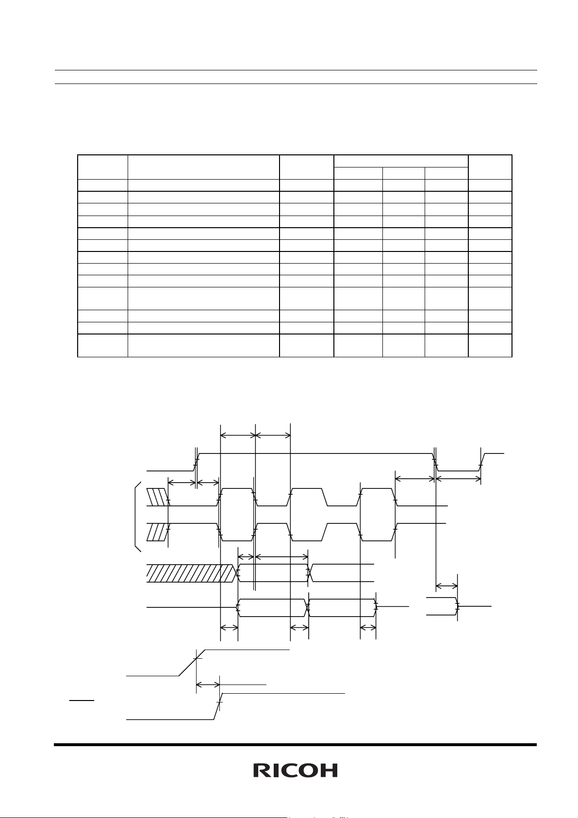
AC ELECTRICAL CHARACTERISTICS
Unless otherwise specified: VSS=0V,Topt=-40 to +85°C
Input and Output Conditions: V
Sym
-bol
t
CE Set-up Time 400 ns
CES
t
CE Hold Time 400 ns
CEH
tCR CE Recovery Time 62
f
SCLK Clock Frequency 1.0 MHz
SCLK
t
SCLK Clock ”H” Time 400 ns
CKH
t
SCLK Clock ”L” Time 400 ns
CKL
t
SCLK Set-up Time 200 ns
CKS
tRD Data Output Delay Time 300 ns
tRZ Data Output Floating Time 300 ns
t
Data Output Delay Time After
CEZ
Falling of CE
tDS Input Data Set-up Time 200 ns
tDH Input Data Hold Time 200 ns
t
Output Delay Time of Voltage
DELAY
Detector
*1) VCC voltage interfacing with CPU is defined by Vaccess (P.5 RECOMMENDED OPERATING
CONDITIONS)
*) For reading/writing timing, see “P.
Writing Time Data under special condition”.
IH=0.8×VCC,VIL=0.2×VCC,VOH=0.8×VCC,VOL=0.2×VCC,CL=50pF
Item Condi-
Tions
V
DD≥1.7V *1)
Min. Typ. Max.
300 ns
Time
Keeping
100 105 110 ms
30 Interfacing with the CPU •Considerations in Reading and
t
t
CKH
CKL
Unit
μs
CE
SCLK
SIO(write cycle)
SIO(read cycle)
VCC
VDCC
t
+VDET1
CKS
t
CES
tRD
t
t
DELAY
DS
t
CEH
tCR
t
DH
t
CEZ
t
RD
t
RZ
9
R2061 series
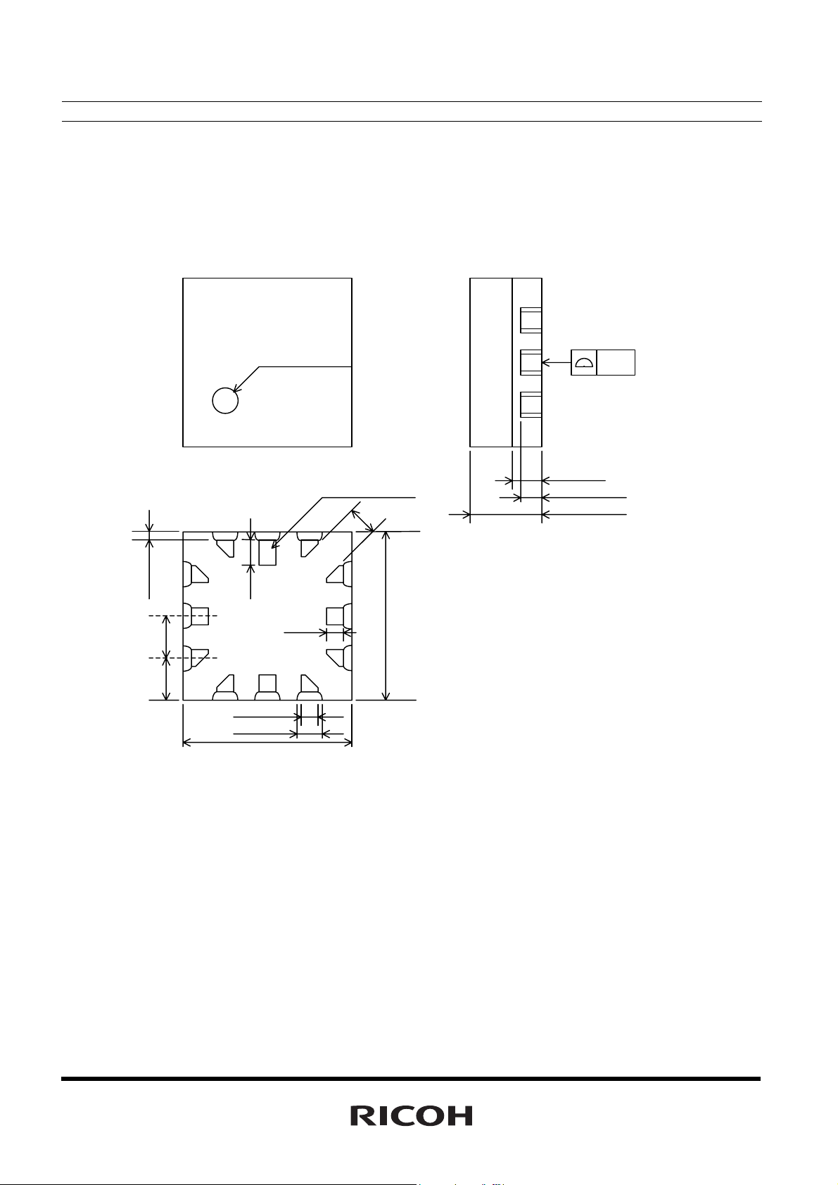
PACKAGE DIMENSIONS
• R2061Kxx
9 7
10
12
0.103
0.5
0.5
1PIN INDEX
3 1
2PIN INDEX
0.15
±
0.3
0.2±0.15
(BOTTOM VIEW)
6
4
0.35
0.1
±
2.0
0.05
0.35
0.25
1.0Max
10
0.17±0.1
0.27±0.15
2.0±0.1
unit: mm
05
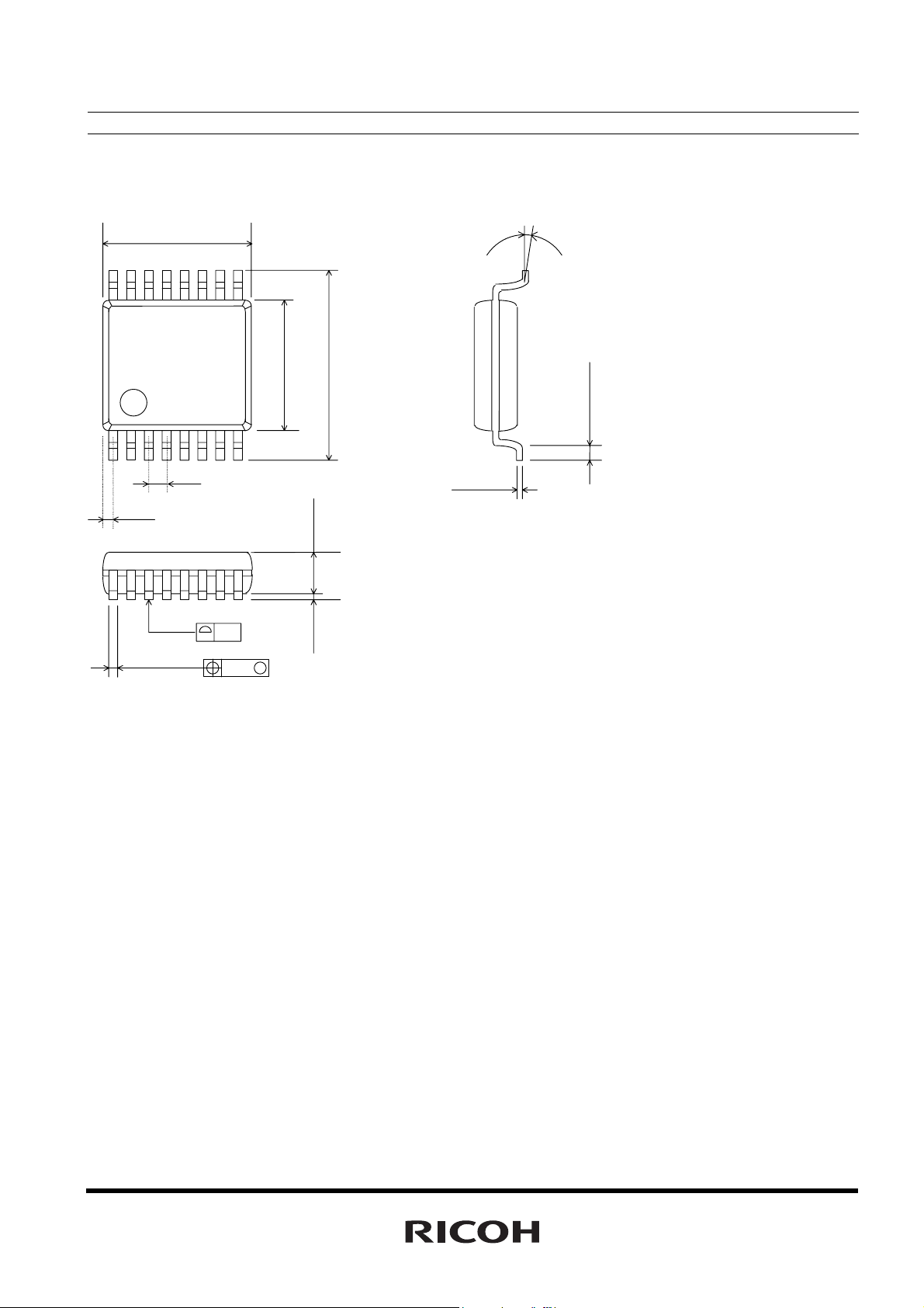
• R2061Sxx
5.0±0.3
R2061 series
0 to 10°
16
1
0.225typ
0.22
+0.1
-0.05
0.65
0.10
0.15
9
0.3
±
4.4±0.2
6.4
8
1.15±0.1
0.1±0.1
M
TAPING SPECIFICATION
0.15
+0.1
-0.
0.3
±
0.5
unit: mm
The R2061 Series have one designated taping direction. The product designation for the taping components is
"R2061S/Kxx-E2".
11
R2061 series
GENERAL DESCRIPTION
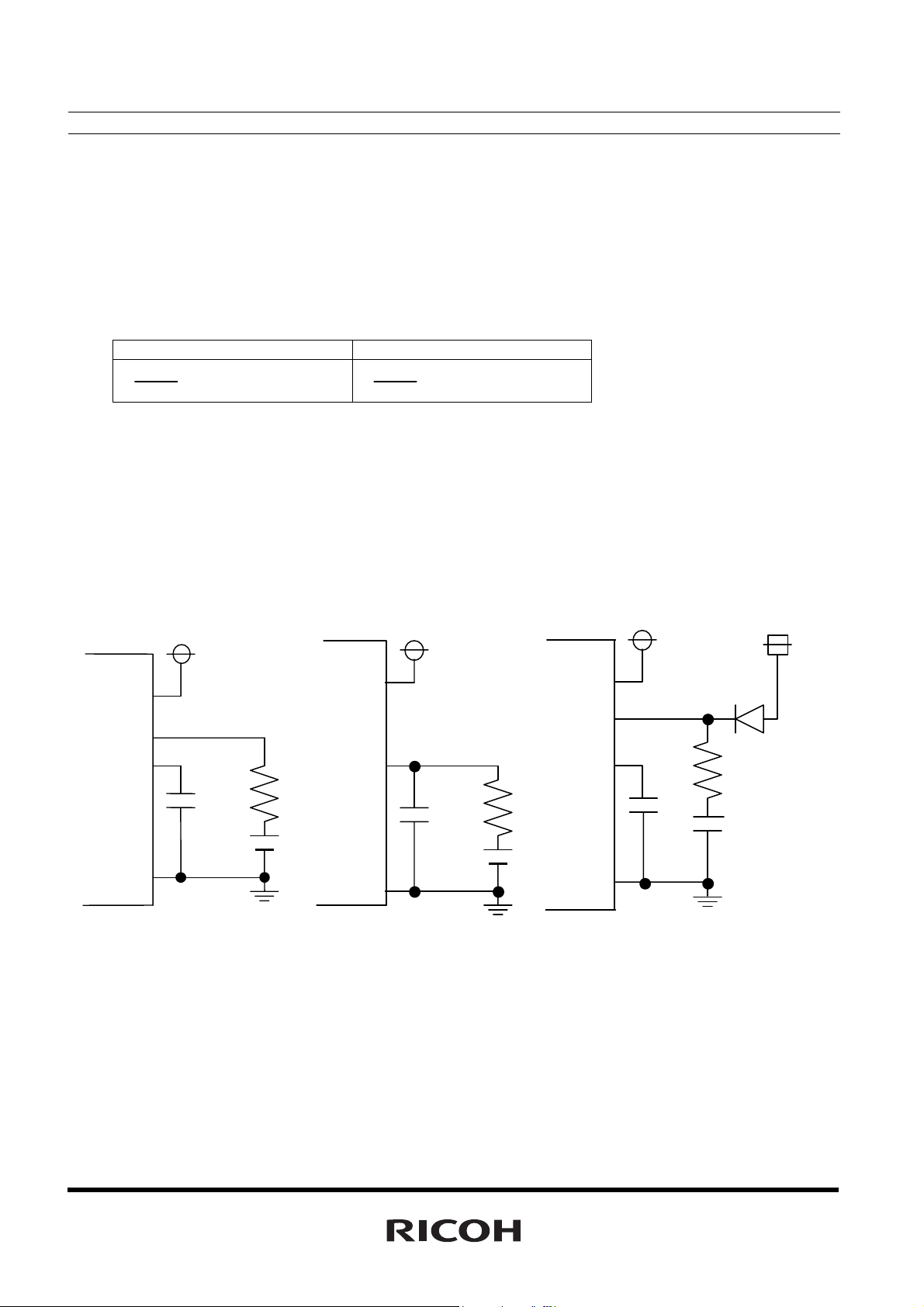
• Battery Backup Switchover Function
The R2061 Series have two power supply input, or VCC and VSB. With monitoring VCC pin input voltage, whi ch
voltage between the two is supplied to the internal power supply is decided.
Refer to the next table to see the state of the backup battery and internal power supply’s state of the IC by each
condition.
V
CC≥VDET1 VCC<VDET1
VCC→RTC, VDD
VDCC
=OFF(H)
As a backup battery, not only a primary battery such as CR2025, LR44, or a secondary battery such as ML614,
TC616, but also an electric double layered capacitor or an aluminum capacitor can be used. Switchover point is
judged with the voltage of the main power (VCC), therefore, if the backup voltage is higher than main supply
voltage, switchover can be realized without extra load to the backup power supply.
The case of back-up by
primary battery
The case of back-up by
capacit or or secondary battery
(Charging voltage is equal to CPU
power supply voltage)
VSB→RTC, VDD
VDCC
=L
The case of back - up by
capacitor or secondary batt er y
(Charging voltage is not equal to
CPU power supply voltage)
VCC
VSB
VDD
VSS
CPU Power
Supply
0.1μF
CR2025
etc.
VCC
VSB
VDD
VSS
CPU power
supply
0.1μF
ML614
etc.
VCC
VSB
VDD
VSS
CPU power
supply
(3V)
0.1μF
5V
Double layer
capacitor
etc.
• Interface with CPU
The R2061 is connected to the CPU by three signal lines CE (Chip Enable), SCLK (Serial Clock), and SIO
(Serial Input / Output), through which it reads and writes data from and to the CPU. The CPU can be accessed
when the CE pin is held high. Acc ess cloc k pulses have a maximu m freque ncy of 1 MHz, allowi ng high-s peed
data transfer to the CPU. VCC falls down under -V
DET1, the R2061 stops accessing with CPU.
12

R2061 series
• Clock and Calendar Function
The R2061 reads and writes time data from and to the CPU in units ranging from secon ds to the last two digi ts of
the calendar year. The calendar year will automatically be identified as a leap year when its last two digits are a
multiple of 4. Consequently, leap years up to the year 2099 can automatically be identified as such.
*) The year 2000 is a leap year while the year 2100 is not a leap year.
• Alarm Function
The R2061 incorporates the alarm interrupt circuit configured to generate interrupt signals to the CPU at preset
times. The alarm interrupt circuit allows two types of alarm settings specified by the Alarm_W registers and the
Alarm_D registers. The Alarm_W registers allow week, hour, and minute alarm settings including combinations
of multiple day-of-week settings such as "Monday, Wednesday, and Friday" and "Saturday and Sunday". The
Alarm_D registers allow hour and minute alarm settings. The Alarm_W outputs from
Alarm_D outputs also from
function.
INTR
pin. Each alarm function can be checked from the CPU by using a polling
INTR
pin, and the
• High-precision Oscillation Adjustment Function
The R2061 has built-in oscillation stabilization capacitors (CG and CD), that can be connected to an external
quartz crystal unit to configure an oscillation circuit. Two kinds of accuracy for this function are alternatives. To
correct deviations in the oscillator frequency of the crystal, the oscillation adjustment circuit is configured to allow
correction of a time count gain or loss (up to ±1.5ppm or ±0.5ppm at 25°C) from the CP U. The maximum range is
approximately ±189ppm (or ±63ppm) in increments of approximately 3ppm (or 1ppm). Such oscillation
frequency adjustment in each system has the following advantages:
* Allows timekeeping with much higher precision than conventional RTCs while using a quartz crystal unit with
a wide range of precision variations.
* Corrects seasonal frequency deviations through seasonal oscillation adjustment.
* Allows timekeeping with higher precision particularly with a temperature sensing function out of RTC, through
oscillation adjustment in tune with temperature fluctuations.
• Power-on Reset, Oscillation Halt Sensing Function and Supply Voltage Monitoring Function
The R2061 has 3 power supply pins (VCC, VSB, VDD), among them, VCC pin and VDD pin have monitoring
function of supply voltage. VCC power supply monitoring circuit make s
pin becomes equal or lower than –V
after the delay time, t
The R2061 incorporates an oscillation halt sensing circuit equipped with internal registers configured to record
any past oscillation halt, the oscillation halt sensing circuit, VDD monitoring flag, and power-on reset flag are
useful for judging the validity of time data.
Power on reset function reset the control resisters when the system is powered on from 0V. At the same time, the
fact is memorized to the resister as a flag, thereby identifying whether they are powered on from 0V or battery
backed-up.
The R2061 also incorporates a supply voltage monitoring circuit equipped with internal registers configured to
record any drop in supply voltage below a certain threshold value. Supply voltage monitoring threshold settings
can be selected between 2.1V and 1.35V through internal register settings. The sampling rate is normally 1s.
DELAY from when the VCC power supply pin becomes equal or more than +VDET1.
DET1. At the power-on of VCC, this circuit makes
VDCC
pin “L” when VCC power supply
VDCC
pin turn off, or “H”
13

R2061 series
The oscillation halt sensing circuit is configured to confirm the established invalidation of time data in contrast to
the supply voltage monitoring circuit intended to confirm the potential invalidation of time data. Further, the
supply voltage monitoring circuit can be applied to battery supply voltage monitoring.
• Periodic Interrupt Function
The R2061 incorporates the periodic interrupt circuit configured to generate periodic interrupt signals aside from
interrupt signals generated by the periodic interrupt circuit for output from the
signals have five selectable frequency settings of 2 Hz (once per 0.5 seconds), 1 Hz (once per 1 second), 1/60
Hz (once per 1 minute), 1/3600 Hz (once per 1 hour), and monthly (the first day of every month). Further,
periodic interrupt signals also have two selectable waveforms, a normal pulse form (with a freq uency of 2 Hz or 1
Hz) and special form adapted to interruption from the CPU in the level mode (with second, minute, hour, and
month interrupts). The condition of periodic interrupt signals ca n be monitored with using a polling function.
INTR
pin. Periodic interrupt
14
R2061 series
A
A
A
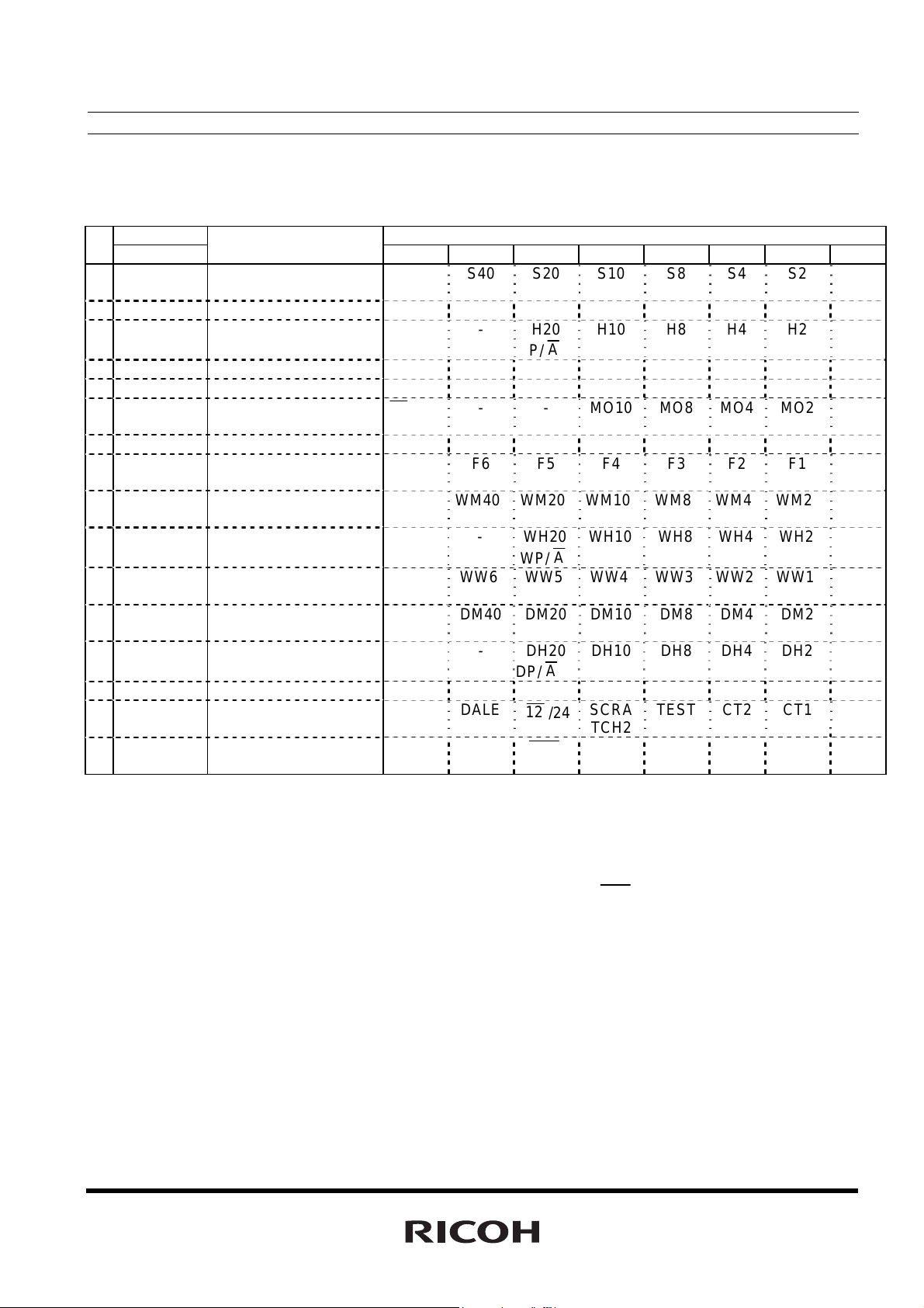
Address Mapping
Address Register Name D a t a
A3A2A1A0 D7 D6 D5 D4 D3 D2 D1 D0
0 0 0 0 0 Second Counter -
*2)
1 0 0 0 1 Minute Counter - M40 M20 M10 M8 M4 M2 M1
2 0 0 1 0 Hour Counter - - H20
3 0 0 1 1 Day-of-week Counter - - - - - W4 W2 W1
4 0 1 0 0 Day-of-month Counter - - D20 D10 D8 D4 D2 D1
5 0 1 0 1 Month Counter and
Century Bit
6 0 1 1 0 Year Counter Y80 Y40 Y20 Y10 Y8 Y4 Y2 Y1
7 0 1 1 1 Oscillation Adjustment
Register *3)
8 1 0 0 0 Alarm_W
(Minute Register)
9 1 0 0 1 Alarm_W
(Hour Register)
A 1 0 1 0 Alarm_W
(Day-of-week Register)
B 1 0 1 1 Alarm_D
(Minute Register)
C 1 1 0 0 Alarm_D
(Hour Register)
D 1 1 0 1 - - - - - - - -
E 1 1 1 0 Control Register 1 *3) WALE DALE
F 1 1 1 1 Control Register 2 *3) VDSL VDET
Notes:
* 1) All the data listed above accept both reading and writing.
* 2) The data marked with "-" is invalid for writing and reset to 0 for reading.
* 3) When the PON bit is set to 1 in Control Register 2, all the bits are reset to 0 in Oscillation Adjustment
Register, Control Register 1 and Control Register 2 excluding the
* 4) When DEV=0, the oscillation adjustment circuit is configured to allow correction of a time count gain
or loss up to ±1.5ppm.
When DEV=1, the oscillation adjustment circuit is configured to allow correction of a time count gain
or loss up to or ±0.5ppm.
* 5) PON is a power-on-reset flag.
19
/20
DEV
*4)
- WM40 WM20 WM10 WM8 WM4 WM2 WM1
- - WH20
- WW6 WW5 WW4 WW3 WW2 WW1 WW0
- DM40 DM20 DM10 DM8 DM4 DM2 DM1
- - DH20
S40 S20 S10 S8 S4 S2 S1
H10 H8 H4 H2 H1
P/
- - MO10 MO8 MO4 MO2 MO1
F6 F5 F4 F3 F2 F1 F0
WH10 WH8 WH4 WH2 WH1
WP/
DH10 DH8 DH4 DH2 DH1
DP/
12
XST
/24
SCRA
TCH2
PON
*5)
XST
TEST CT2 CT1 CT0
SCRA
TCH1
bit.
CTFG WAFG DAFG
15
R2061 series
Register Settings
• Control Register 1 (ADDRESS Eh)
D7 D6 D5 D4 D3 D2 D1 D0
WALE DALE
WALE DALE
0 0 0 0 0 0 0 0 Default Settings *)
*) Default settings: Default value means read / written values when the PON bit is set to “1” due to VDD
power-on from 0 volts.
12
12
/24
/24
(1) WALE, DALE Alarm_W Enable Bit, Alarm_D Enable Bit
WALE,DALE Description
0 Disabling the alarm interrupt circuit (under the control of the settings
of the Alarm_W registers and the Alarm_D registers).
1 Enabling the alarm interrupt circuit (under the control of the settings
of the Alarm_W registers and the Alarm_D registers)
12
(2)
Setting the
Setting the
/24
12
/24
0 Selecting the 12-hour mode with a.m. and p.m. indications. (Default)
1 Selecting the 24-hour mode
12
/24 bit to 0 and 1 specifies the 12-hour mode and the 24-hour mode, respectively.
24-hour mode 12-hour mode 24-hour mode 12-hour mode
00 12 (AM12) 12 32 (PM12)
01 01 (AM 1) 13 21 (PM 1)
02 02 (AM 2) 14 22 (PM 2)
03 03 (AM 3) 15 23 (PM 3)
04 04 (AM 4) 16 24 (PM 4)
05 05 (AM 5) 17 25 (PM 5)
06 06 (AM 6) 18 26 (PM 6)
07 07 (AM 7) 19 27 (PM 7)
08 08 (AM 8) 20 28 (PM 8)
09 09 (AM 9) 21 29 (PM 9)
10 10 (AM10) 22 30 (PM10)
11 11 (AM11) 23 31 (PM11)
12
/24 bit should precede writing time data
12
/24-hour Mode Selection Bit
(3) SCRATCH2 Scratch Bit 2
SCRATCH2 Description
0 (Default)
1
The SCRATCH2 bit is intended for scratching and accepts the reading and writing of 0 and 1.
The SCRATCH2 bit will be set to 0 when the PON bit is set to 1 in the Control Register 1.
SCRA
TCH2
SCRA
TCH2
TEST CT2 CT1 CT0 (For Writing)
TEST CT2 CT1 CT0 (For Reading)
(Default)
Description
16
R2061 series
A
(4) TEST Test Bit
TEST Description
0 Normal operation mode. (Default)
1 Test mode.
The TEST bit is used only for testing in the factory and should normally be set to 0.
(5) CT2,CT1, and CT0 Periodic Interrupt Selection Bits
Description CT2 CT1 CT0
Wave form
mode
0 0 0 - OFF(H) (Default)
0 0 1 - Fixed at “L”
0 1 0 Pulse Mode
*1)
0 1 1 Pulse Mode
*1)
1 0 0 Level Mode
*2)
1 0 1 Level Mode
*2)
1 1 0 Level Mode
*2)
1 1 1 Level Mode
*2)
* 1) Pulse Mode: 2-Hz and 1-Hz clock pulses are output in synchronization with the increment of the
second counter as illustrated in the timing chart below.
Interrupt Cycle and Falling Timing
2Hz(Duty50%)
1Hz(Duty50%)
Once per 1 second (Synchronized with
second counter increment)
Once per 1 minute (at 00 seconds of
every minute)
Once per hour (at 00 minutes and 00
seconds of every hour)
Once per month (at 00 hours, 00 minutes,
and 00 seconds of first day of every
month)
CTFG Bit
IN T R
Pin
pprox. 92μs
(Increment of second counter)
Rewriting of the second counter
In the pulse mode, the increment of the second counter is delayed by approximately 92 μs from the falling
edge of clock pulses. Consequently, time readings immediately after the falling edge of clock pulses may
appear to lag behind the time counts of the real-time clocks by approximately 1 second. Rewriting the
second counter will reset the other time counters of less than 1 second, driving the
INTR
pin low.
* 2) Level Mode: Periodic interrupt signals are output with selectable interrupt cycle settings of 1 second,
1 minute, 1 hour, and 1 month. The increment of the second counter is synchronized with the falling
edge of periodic interrupt signals. For example, periodic interrupt signals with an interrupt cycle setting
of 1 second are output in synchronization with the increment of the second counter as illustrated in the
timing chart below.
17
R2061 series
CTFG Bit
IN T R
Pin
Setting CTFG bit to 0
(Increment of
second counter)
(Increment of
second counter)
Setting CTFG bit to 0
(Increment of
second counter)
*1), *2) When the oscillation adjustment circuit is used, the interrupt cycle will fluctuate once per 20sec. or
60sec. as follows:
Pulse Mode: The “L” period of output pulses will increment or decrement by a maximum of ±3.784 ms. For
example, 1-Hz clock pulses will have a duty cycle of 50 ±0.3784%.
Level Mode: A periodic interrupt cycle of 1 second will increment or decrement by a maximum of
±3.784 ms.
18
 Loading...