


R2045S/D
4-wire Serial Interface Real Time Clock Module
NO.EA-113-100825
OUTLINE
The R2045S/D is a real-time clock module, built in CMOS real-time clock IC and crystal oscillator, connected to
the CPU by four signal lines, CE, SCLK, SI, and SO, and configured to perform serial transmission of time and
calendar data to the CPU. The oscillation frequency is adjusted to high precision (0±5ppm: 15sec. per month at
25°C) The periodic interrupt circuit is configured to generate interrupt signals with six selectable interrupts
ranging from 0.5 seconds to 1 month. The 2 alarm interrupt circuits generate interrupt signals at preset times. As
the oscillation circuit is driven under constant volt age, fluctuation of the oscillator frequency due to supply volt age
is small, and the time keeping current is small (TYP. 0.48μA at 3V). The oscillation halt sensing circuit can be
used to judge the validity of internal data in such events as power-on; The supply voltage monitoring circuit is
configured to record a drop in supply voltage below two selectable supply voltage monitoring threshold settings.
The 32-kHz clock output function (N-channel Open drain output) is intended to output sub-clock pulses for the
external microcomputer. The oscillation adjustment circuit is intended to adjust time by correcting deviations in
the oscillation frequency of the crystal oscillator.
FEATURES
• Built in 32.768kHz crystal unit, The oscillation frequency is adj usted to high precision (0±5ppm: at 25°C)
• Time keeping voltage 1.15V to 5.5V
• Super low power consumption 0.48μA TYP (1.2μA MAX) at V
• Four signal lines (CE, SCLK, SI, and SO) required for connection to the CPU.
• Time counters (counting hours, minutes, and seconds) and calendar counters (counting years, months,
days, and weeks) (in BCD format)
• Interrupt circuit configured to generate interrupt signals (with interrupts ranging from 0.5 seconds to 1
month) to the CPU and provided with an interrupt flag and an interrupt halt
• 2 alarm interrupt circuits (Alarm_W for week, hour, and minute alarm settings and Alarm_D for hour and
minute alarm settings)
• 32768Hz clock output pin (N-channel open drain output)
• With Power-on flag to prove that the power supply starts from 0V
• With Oscillation halt sensing Flag to judge the validity of internal data
• Supply voltage monitoring circuit with two supply voltage monitoring threshold settings
• Automatic identification of leap years up to the year 2099
• Selectable 12-hour and 24-hour mode settings
• Oscillation adjustment circuit for correcting temperature frequency deviation or offset deviation
• CMOS process
• Two types of p ackage, SOP14(10.1x7.4x3.1) or SON22(6.1x5.0x1.3)
DD=3V
1
R2045S/D
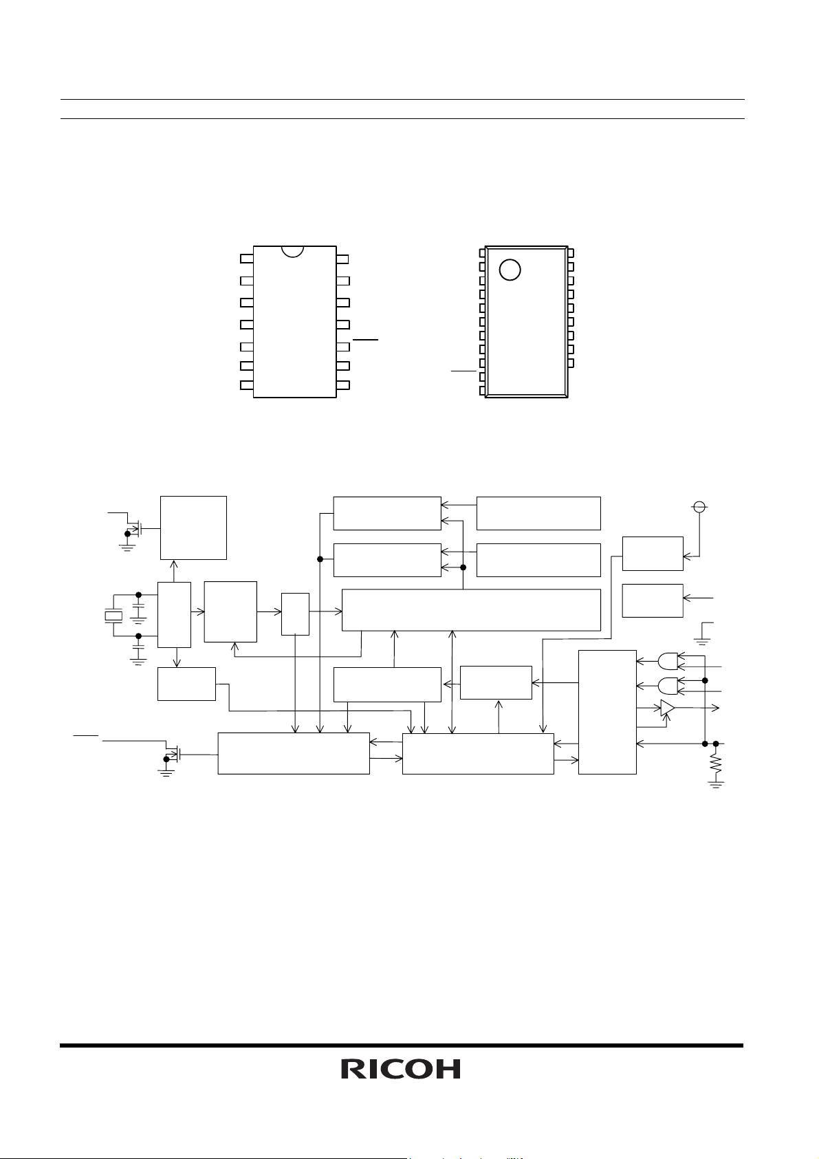
PIN CONFIGURATION
32KOUT
R2045S (SOP14)
N.C.
SCLK SO
N.C.
VPP
VDD N.C.
1
2
3
4
5
6
7
TOP VIEW
BLOCK DIAGRAM
14
13
12
11
10
N.C.
SI
VSS
INTR
9
N.C. CE
8
R2045D (SON22)
CE
1
VDD
2
N.C. N.C.
3
VPP
SO
VSS
INTR
N.C.
4
5
6
7
SI
8
9
10
11
32KOUT
SCLK
TOP VIEW
22
21
20
19
18
17
16
15
14
N.C.
N.C.
N.C.
N.C.
N.C.
N.C.
N.C.
N.C.
32KOUT
INTR
32kHz
OUTPUT
CONTROL
OSC
OSC
DETECT
DIVIDER
CORREC
-TION
INTERRUPT CONTROL
DIV
COMPARATOR_W
COMPARATOR_D
(SEC,MIN,HOUR,WEEK,DAY,MONTH,YEAR)
ADDRESS
DECODER
TIME COUNTER
SHIFT REGISTER
ALARM_W REGISTER
(MIN,HOUR, WEEK)
ALARM_D REGISTER
(MIN,HOUR)
ADDRESS
REGISTER
I/O
CONTROL
VOLTAGE
DETECT
TEST
CIRCUIT
VDD
VPP
VSS
SCLK
SI
SO
CE
2

PIN DESCRIPTION
Symbol Item Description
CE Chip enable
Input
SCLK Serial Clock
Input
SI Serial Input The SI pin is used to input data intended for writing in synchronization with
SO Serial
Output
INTR
32KOUT 32kHz Clock
VDD Positive
VSS Negative
VPP Test input This pin is power pin for testing in the factory. Please don’t connect to any
N.C. No
Interrupt
Output
Output
Power
Supply Input
Power
Supply Input
Connection
The CE pin is used for interfacing with the CPU. Should be held high to
allow access to the CPU. Incorporates a pull-down resistor. Should be
held low or open when the CPU is powered off. Allows a maximum input
voltage of 5.5v regardless of supply voltage.
The SCLK pin is used to input clock pulses synchronizing the input and
output of data to and from the SI and SO pins. Allows a maximum input
voltage of 5.5v regardless of supply voltage.
the SCLK pin. CMOS input. Allows a maximum input voltage of 5.5v
regardless of supply voltage.
The SO pin is used to output data intended for reading in synchronization
with the SCLK pin. CMOS output.
INTR
The
interrupt (Alarm_D) and output periodic interrupt signals to the CPU sign als.
Disabled at power-on from 0V. N-channel open drain output. Allows a
maximum pull-up voltage of 5.5v regardless of supply voltage.
The 32KOUT pin is used to output 32.768-kHz clock pulses. And controlled
by resister setting. When VDD power-on from 0v, this output is enabled.
The pin is N-channel open drain output. Allows a maximum pull-up voltage
of 5.5v regardless of supply voltage.
The VDD pin is connected to the power supply.
The VSS pin is grounded.
other pins.
These pins are not connected to internal IC chip.
In R2045D (SON22), N.C. pins from 14 pin to 22 pin are connected together
internally. Never connect these pins to any lines, or connect to VDD or
VSS. And never connect different voltage level lines each other.
pin is used to output alarm interrupt (Alarm_W) and alarm
R2045S/D
3
R2045S/D
ABSOLUTE MAXIMUM RATINGS
(VSS=0V)
Symbol Item Pin Name and Condition Description Unit
VDD Supply Voltage VDD -0.3 to +6.5 V
Input Voltage 1 CE, SCLK, SI -0.3 to +6.5 VI
Input Voltage 2 VPP -0.3 to V
Output Voltage 1 SO -0.3 to VDD+0.3 VO
Output Voltage 2
PD Power Dissipation
Topt Operating
Temperature
Tstg Storage Temperature -55 to +125
INTR
, 32KOUT
Topt=25°C
-40 to +85
-0.3 to +6.5
300 mW
DD+0.3
V
V
°C
°C
RECOMMENDED OPERATING CONDITION
(VSS=0V, Topt=-40 to +85°C)
Symbol Item Pin Name and Condition Min. Typ. Max. Unit
VACCESS Supply Voltage VDD power supply voltage
for interfacing with CPU
VCLK Time Keeping Voltage 1.15 5.5 V
VPUP Pull-up Voltage
INTR
1.7 5.5 V
5.5 V
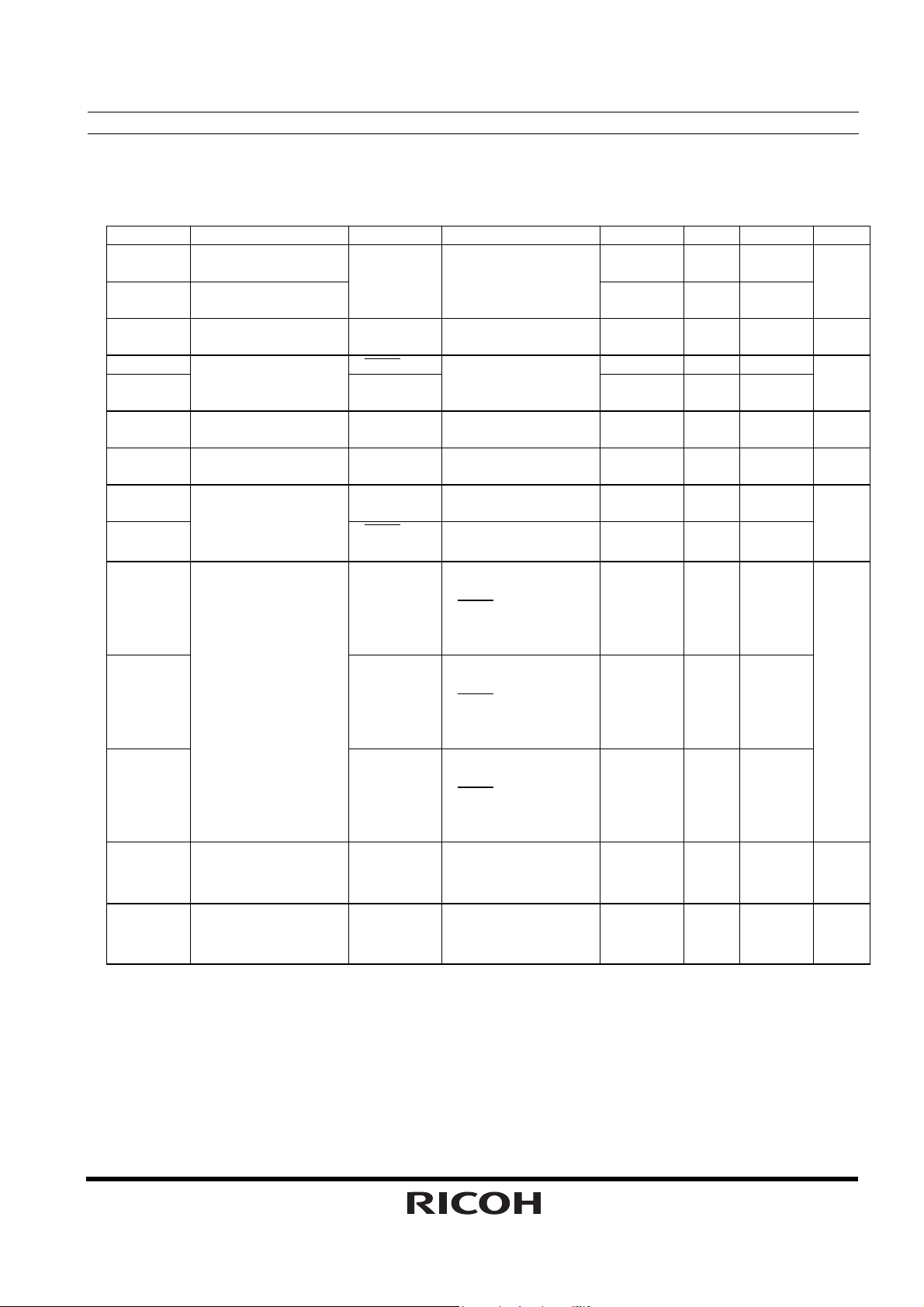
FREQUENCY CHARACTERISTICS
(VSS=0V)
Symbol Item Condition Min. Typ. Max. Unit
Δf/f0
Fv Frequency
Top Frequency
tsta Oscillation
fa Aging
Frequency
Deviation
Voltage
Characteristics
Temperature
Characteristics
Start-up Time
Topt=25°C, VDD=3V
Topt=25°C,
DD=2.0V to 5.5V
V
Topt=-20°C to +70°C
25°C as standard
Topt=25°C, V
Topt=25°C, V
First year
DD=2V
DD=3V,
-5 0 +5 ppm
-1 +1 ppm
-120 +10 ppm
+1 sec
-5 +5 ppm
4
R2045S/D
DC ELECTRICAL CHARACTERISTICS
Unless otherwise specified: VSS=0V,VDD=3V,Topt=-40 to +85°C
Symbol Item Pin Name Condition Min. Typ. Max. Unit
VIH “H” Input Voltage 0.8x
CE,
DD=1.7 to 5.5V
V
SCLK,
VIL “L” Input Voltage
IOH “H” Output
SI
SO VOH=VDD-0.5V -0.5 mA
Current
IOL1
IOL2
“L” Output Current
INTR
SO,
OL=0.4V
V
32KOUT
IIL Input Leakage
Current
RDNCE Pull-down
SCLK, SI VI=5.5V or VSS
DD=5.5V
V
CE 40 120 400
Resistance
IOZ1 SO VO=5.5V or VSS
IOZ2
IDD1
Output Off-state
Leakage Current
Time Keeping
Current
INTR
,
32KOUT
VDD
VDD=5.5V
VO=5.5V
VDD=3V,
CE, SCLK, SI, SO,
INTR
, 32KOUT
SS
=V
32KOUT disabled
IDD2
VDD
VDD=5V,
CE, SCLK, SI, SO,
INTR
, 32KOUT
SS
=V
32KOUT disabled
IDD3
VDD VDD=3V,
CE, SCLK, SI, SO,
INTR
, 32KOUT
SS
=V
32KOUT enabled
V
V
DETH
DETL
Supply Voltage
Monitoring Voltage
(“H”)
Supply Voltage
Monitoring Voltage
(“L”)
VDD
VDD
Topt=-30 to +70°C
Topt=-30 to +70°C
DD
V
-0.3 0.2x
2.0
0.5
-1.0 1.0
-1.0 1.0
-1.0 1.0
0.65 2.00
1.90
1.15
5.5
DD
V
0.48 1.20
0.60 1.80
2.10 2.30
1.30 1.45
V
mA
μA
kΩ
μA
μA
V
V
5
R2045S/D
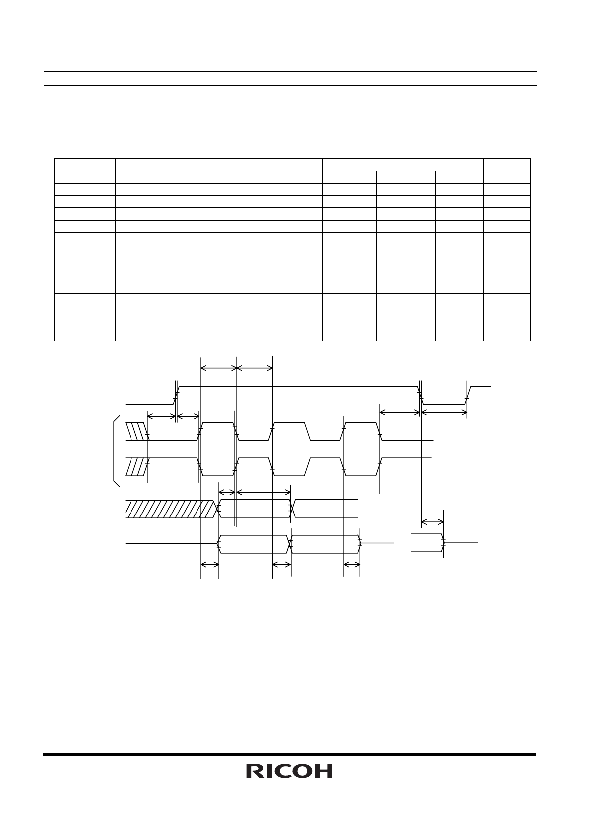
K
AC ELECTRICAL CHARACTERISTICS
Unless otherwise specified: VSS=0V,Topt=-40 TO +85°C
Input / Output condition: V
Symbol Item Condi-
t
CE Set-up Time 400 ns
CES
t
CE Hold Time 400 ns
CEH
tCR CE Recovery Time 62
f
SCLK Clock Frequency 1.0 MHz
SCLK
t
SCLK Clock High Time 400 ns
CKH
t
SCLK Clock Low Time 400 ns
CKL
t
SCLK Set-up Time 200 ns
CKS
tRD Data Output Delay Time 300 ns
tRZ Data Output Floating Time 300 ns
t
Data Output Delay Time
CEZ
After Falling of CE
tDS Input Data Set-up Time 200 ns
tDH Input Data Hold Time 200 ns
IH=0.8xVDD,VIL=0.2xVDD,VOH=0.8xVDD,VOL=0.2xVDD,CL=50pF
V
DD≥1.7V
tions
Min. Typ. Max.
300 ns
t
CKH
t
CKL
Unit
μs
CE
t
CKS
SCL
SI
SO
*) For reading/writing timing, see “P.
condition”.
t
CES
t
CEH
t
CEZ
tCR
t
DS
t
DH
tRD
t
RD
t
RZ
26 •Considerations in Reading and W riting Time Data under special
6
#
#7 #1 #
A
A
A
A
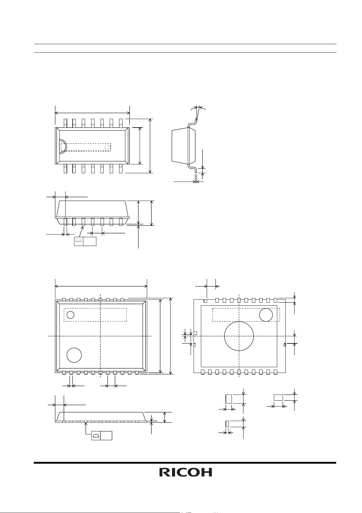
PACKAGE DIMENSIONS
• R2045S (SOP14)
1.24typ.
10.1±0.2
0.1
±
6.1
1.27±0.1
0.2
8
5.0±0.2
7.4±0.2
0.1
±
3.2
3.1typ.
-0.05
+0.1
0.1
14
+0.1
0.35
-0.05
• R2045D (SON22)
#22 #14
0°-10
0.15
°
+0.1
-0.05
0.65
0.25
±
0.6
R2045S/D
#22 #14
’
0.1
±
0.3
5.0
0.05
B
0.43
’
0.2
0.1
±
B
0.3
B
0.43
#1 #11
0.3
0.2
0.1
0.2
0.2
0.2
±
±
4.7
0.1
0.2
±
0.5
0.1
±
#1 #11
0.55typ.
1.3
+0.1/-0.05
0.125
0.1
7

R2045S/D
GENERAL DESCRIPTION
• Interface with CPU
The R2045S/D is connected to the CPU by four signal lines CE (Chip Enable), S CLK (Serial Clock), SI (Serial
Input), and SO (Serial Output), through which it reads and writes data from and to the CPU. The CPU can be
accessed when the CE pin is held high. Access clock pulses have a maximum frequency of 1 MHz allowing
high-speed data transfer to the CPU.
• Clock and Calendar Function
The R2045S/D reads and writes time data from and to the CPU in units ranging from seconds to the last two
digits of the calendar year. The calendar year will automatically be identified as a leap year when its last two
digits are a multiple of 4. Consequently , leap years u p to the year 2099 can automatically be identified as such.
• Alarm Function
The R2045S/D incorporates the alarm interrupt circuit configured to generate interrupt signals to the CPU at
preset times. The alarm interrupt circuit allows two types of alarm settings specified by the Alarm_W registers
and the Alarm_D registers. The Alarm_W registers allow week, hour, and minute alarm settings including
combinations of multiple day-of-week settings such as "Monday, Wednesday, and Friday" and "Saturday and
Sunday". The Alarm_D registers allow hour and minute alarm settings. The Alarm_W outputs from
pin, and the Alarm_D output s also from
a polling function.
INTR
pin. Each alarm function can be checked from the CPU by using
High-precision Oscillation Adjustment Function
INTR
To correct deviations in the oscillation frequency of the crystal oscillator, the oscillation adjustment circuit is
configured to allow correction of a time count gain or loss (up to ±1.5 ppm at 25°C) from the CPU within a
maximum range of approximately + 189 ppm in increments of approximately 3 ppm. Such oscillation frequen cy
adjustment in each system has the following advantages:
* Corrects seasonal frequency deviations through seasonal o scillation adjustment.
* Allows timekeeping with higher precision particularly with a temperature sensing function out of RTC,
through oscillation adjustment in tune with temperature fluctuations.
• Oscillation Halt Sensing Flag, Power-on Reset Flag, and Supply Voltage Monitoring Function
The R2045S/D incorporates an oscillation halt sensing circuit equipped with internal registers configured to
record any past oscillation halt.
Power-on reset flag is set to “1” When R2045S/D is powered on from 0V.
As such, the oscillation halt sensing flag and Power-on reset flag are useful for judging the validity of time
data.
The R2045S/D also incorporates a supply voltage monitoring circuit equipped with internal registers
configured to record any drop in supply voltage below a certain threshold value. Supply voltage monitoring
threshold settings can be selected between 2.1 and 1.3 volts through internal register settings. The oscillation
halt sensing circuit is configured to confirm the established invalidation of time data in contrast to the supply
voltage monitoring circuit intended to confirm the potential invalidation of time data. Further, the supply voltage
monitoring circuit can be applied to battery supply voltage monitoring.
8

R2045S/D
• Periodic Interrupt Function
The R2045S/D incorporates the periodic interrupt circuit configured to generate periodic interrupt signals
aside from interrupt signals generated by the periodic interrupt circuit for output from the
interrupt signals have five selectable frequency settings of 2 Hz (once per 0.5 seconds), 1 Hz (once per 1
second), 1/60 Hz (once per 1 minute), 1/3600 Hz (once per 1 hour), and monthly (the first day of every month).
Further, periodic interrupt signals also have two selectable waveforms, a normal pulse form (with a frequency of
2 Hz or 1 Hz) and special form adapted to interruption from the CPU in the level mode (with second, minute, hour,
and month interrupts). The condition of periodic interrupt signals can be monitored by using a polling function.
INTR
pin. Periodic
• 32kHz Clock Output
The R2045S/D incorporates a 32-kHz clock circuit configured to generate clock pulses with the oscillation
frequency of a 32.768kHz crystal oscillator for output from the 32KOUT pin. The 32-kHz clock output can be
disabled by certain register settings but cannot be disabled without manipulation of any two registers with
different addresses to prevent disabling in such event s as the runaway of the CPU.
9
R2045S/D
A
A
A
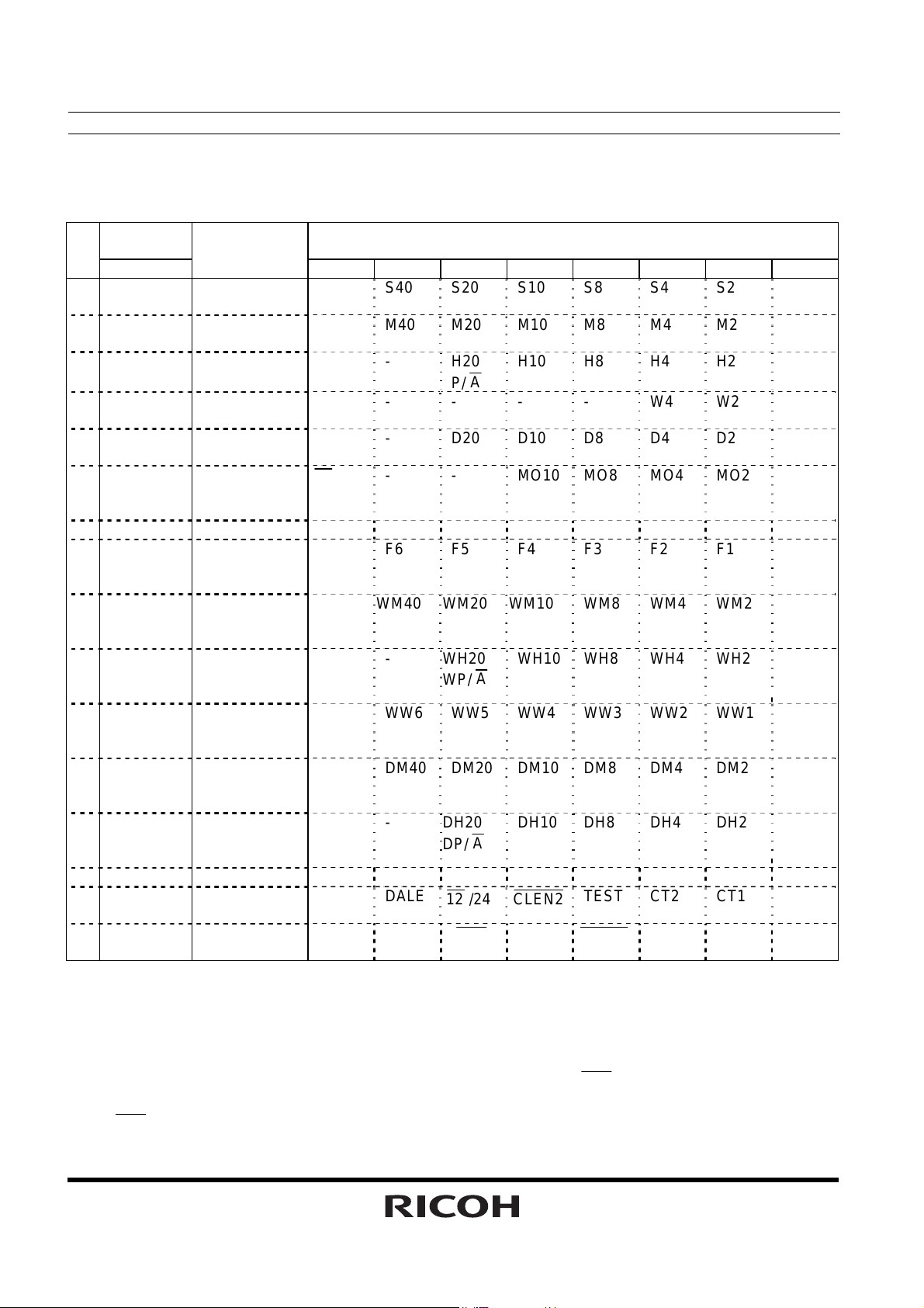
Address Mapping
Address Register
Name
A3A2A1A0 D7 D6 D5 D4 D3 D2 D1 D0
0 0 0 0 0 Second
Counter
1 0 0 0 1 Minute
Counter
2 0 0 1 0 Hour Counter - - H20
3 0 0 1 1 Day-of-week
Counter
4 0 1 0 0 Day-of-month
Counter
5 0 1 0 1 Month
Counter and
Century Bit
6 0 1 1 0 Year Counter Y80 Y40 Y20 Y10 Y8 Y4 Y2 Y1
7 0 1 1 1 Oscillation
Adjustment
Register *3)
8 1 0 0 0 Alarm_W
(Minute
Register)
9 1 0 0 1 Alarm_W
(Hour
Register)
A 1 0 1 0 Alarm_W
(Day-of-week
Register)
B 1 0 1 1 Alarm_D
(Minute
Register)
C 1 1 0 0 Alarm_D
(Hour
Register)
D 1 1 0 1 - - - - - - - E 1 1 1 0 Control
Register 1 *3)
F 1 1 1 1 Control
Register 2 *3)
Notes:
*1) All the data listed above accept both reading and writing.
*2) The data marked with "-" is invalid for writing and reset to 0 for reading.
*3) When the PON bit is set to 1 in Control Register 2, all the bits are reset to 0 in Oscillation Adjustment
Register, Control Register 1 and Control Register 2 excluding the
*4) The (0) bit should be set to 0.
XST
*5)
*6) PON is power-on reset flag.
is oscillation halt sensing bit.
*2)
- M40 M20 M10 M8 M4 M2 M1
- - - - - W4 W2 W1
- - D20 D10 D8 D4 D2 D1
19
/20
(0)
*4)
- WM40 WM20 WM10 WM8 WM4 WM2 WM1
- - WH20
- WW6 WW5 WW4 WW3 WW2 WW1 WW0
- DM40 DM20 DM10 DM8 DM4 DM2 DM1
- - DH20
WALE DALE
VDSL VDET
S40 S20 S10 S8 S4 S2 S1
P/
- - MO10 MO8 MO4 MO2 MO1
F6 F5 F4 F3 F2 F1 F0
12
/24
XST
WP/
DP/
D a t a
H10 H8 H4 H2 H1
WH10 WH8 WH4 WH2 WH1
DH10 DH8 DH4 DH2 DH1
CLEN2
PON
*5)
TEST CT2 CT1 CT0
CLEN1
XST
CTFG WAFG DAFG
and PON bits.
10
R2045S/D
Register Settings
• Control Register 1 (ADDRESS Eh)
D7 D6 D5 D4 D3 D2 D1 D0
WALE DALE
WALE DALE
0 0 0 0 0 0 0 0 Default Settings *)
*) Default settings: Default value means read / written values when the PON bit is set to “1” due to VDD
power-on from 0 volts.
12
12
/24
/24
CLEN2
CLEN2
(1) WALE, DALE Alarm_W Enable Bit, Alarm_D Enable Bit
WALE,DALE Description
0 Disabling the alarm interrupt circuit (under the control of the settings
of the Alarm_W registers and the Alarm_D registers).
1 Enabling the alarm interrupt circuit (under the control of the settings
of the Alarm_W registers and the Alarm_D registers)
12
(2)
(3)
/24
12
/24
0 Selecting the 12-hour mode with a.m. and p.m. indications. (Default)
1 Selecting the 24-hour mode
Setting the
24-hour mode 12-hour mode 24-hour mode 12-hour mode
00 12 (AM12) 12 32 (PM12)
01 01 (AM 1) 13 21 (PM 1)
02 02 (AM 2) 14 22 (PM 2)
03 03 (AM 3) 15 23 (PM 3)
04 04 (AM 4) 16 24 (PM 4)
05 05 (AM 5) 17 25 (PM 5)
06 06 (AM 6) 18 26 (PM 6)
07 07 (AM 7) 19 27 (PM 7)
08 08 (AM 8) 20 28 (PM 8)
09 09 (AM 9) 21 29 (PM 9)
10 10 (AM10) 22 30 (PM10)
11 11 (AM11) 23 31 (PM11)
Setting the
CLEN2
0 Enabling the 32-kHz clock output (Default)
1 Disabling the 32-kHz clock output
Setting the
pulses with the oscillation frequency of the 32.768-kHz crystal oscillator for output from the 32KOUT pin.
Conversely, setting both the
12
/24 bit to 0 and 1 specifies the 12-hour mode and the 24-hour mode, respectively.
12
/24 bit should precede writing time data
32-kHz Clock Output Bit2
CLEN2
CLEN2
bits or the
12
/24-hour Mode Selection Bit
CLEN1
CLEN1
bit (D3 in the control register 2) to 0 specifies generating clock
and the
TEST CT2 CT1 CT0 (For Writing)
TEST CT2 CT1 CT0 (For Reading)
Description
Description
CLEN2
bit to 1 specifies disabling (“H”) such output.
(Default)
11
R2045S/D
A
(4) TEST Test Bit
TEST Description
0 Normal operation mode. (Default)
1 Test mode.
The TEST bit is used only for testing in the factory and should normally be set to 0.
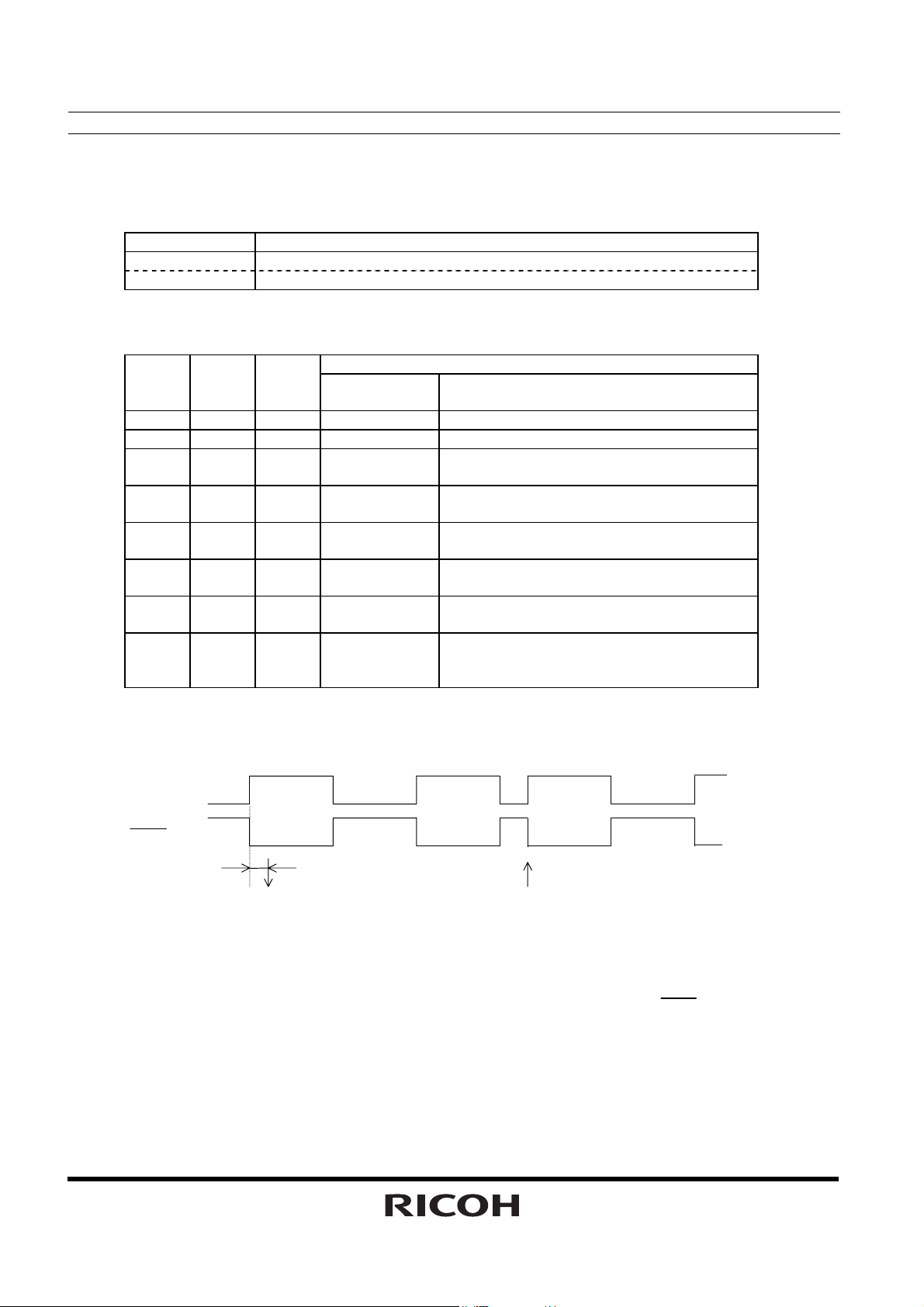
(5) CT2,CT1, and CT0 Periodic Interrupt Selection Bits
Description CT2 CT1 CT0
Wave form
mode
0 0 0 - OFF(H) (Default)
0 0 1 - Fixed at “L”
0 1 0 Pulse Mode
*1)
0 1 1 Pulse Mode
*1)
1 0 0 Level Mode
*2)
1 0 1 Level Mode
*2)
1 1 0 Level Mode
*2)
1 1 1 Level Mode
*2)
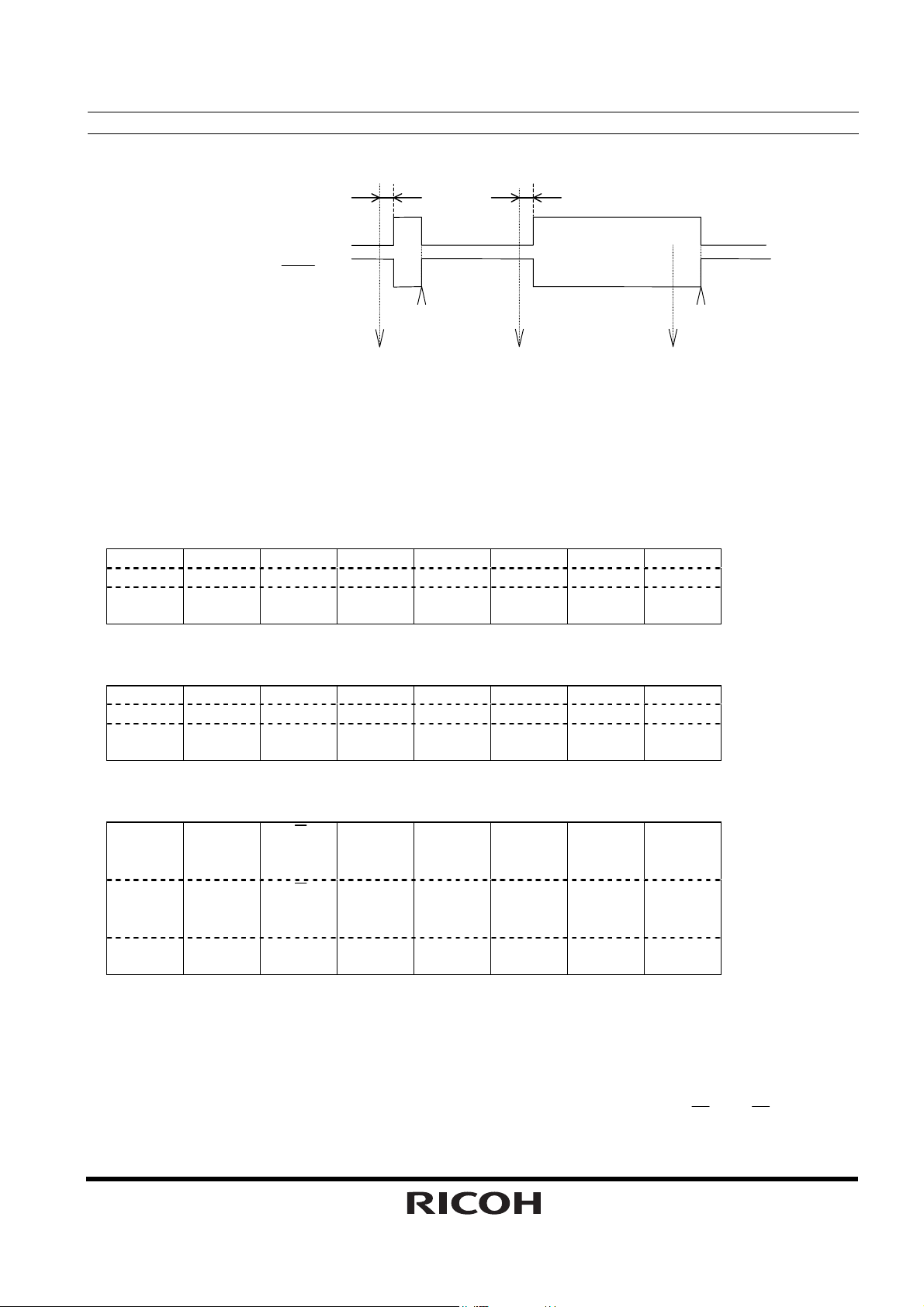
* 1) Pulse Mode: 2-Hz and 1-Hz clock pulses are output in synchronization with the increment of the
second counter as illustrated in the timing chart below.
Interrupt Cycle and Falling Timing
2Hz(Duty50%)
1Hz(Duty50%)
Once per 1 second (Synchronized with
second counter increment)
Once per 1 minute (at 00 seconds of
every minute)
Once per hour (at 00 minutes and 00
seconds of every hour)
Once per month (at 00 hours, 00 minutes,
and 00 seconds of first day of every
month)
12
In the pulse mode, the increment of the second counter is delayed by approximately 92 μs from the falling
edge of clock pulses. Consequently, time readings immediately after the falling edge of clock pulses may
appear to lag behind the time counts of the real-time clocks by approximately 1 second. Rewriting the
second counter will reset the other time counters of less than 1 second, driving the
* 2) Level Mode: Periodic interrupt signals are output with selectable interrupt cycle settings of 1 second,
1 minute, 1 hour, and 1 month. The increment of the second counter is synchronized with the falling edge
of periodic interrupt signals. For example, periodic interrupt signals with an interrupt cycle setting of 1
second are output in synchronization with the increment of the second counter as illustrated in the timing
chart below.
CTFG Bit
IN T R
Pin
pprox. 92μs
(Increment of second counter)
INTR
pin low.
Rewriting of the second counter

R2045S/D
*1), *2) When the oscillation adjustment circuit is used, the interrupt cycle will fluctuate once per 60sec. as
follows:
Pulse Mode:
The “L” period of output pulses will increment or decrement by a maximum of ±3.784 ms. For example,
1-Hz clock pulses will have a duty cycle of 50 ±0.3784%.
Level Mode:
A periodic interrupt cycle of 1 second will increment or decrement by a maximum of ±3.784 ms.
CTFG Bit
IN T R
Pin
(Increment of
second counter)
Setting CTFG bit to 0
(Increment of
second counter)
Setting CTFG bit to 0
(Increment of
second counter)
• Control Register 2 (Address Fh)
D7 D6 D5 D4 D3 D2 D1 D0
VDSL VDET
VDSL VDET
0 0
*) Default settings: Default value means read / written values when the PON bit is set to “1” due to VDD
power-on from 0 volts.
XST
XST
Indefinite
PON
PON
1 0 0 0 0 Default Settings *)
CLEN1
CLEN1
(1) VDSL VDD Supply Voltage Monitoring Threshold Selection Bit
VDSL Description
0 Selecting the VDD supply voltage monitoring threshold setting of 2.1v. (Default)
1 Selecting the VDD supply voltage monitoring threshold setting of 1.3v.
The VDSL bit is intended to select the VDD supply voltage monitoring threshold settings.
(2) VDET Supply Voltage Monitoring Result Indication Bit
VDET Description
0 Indicating supply voltage above the supply voltage monitoring
threshold settings.
1 Indicating supply voltage below the supply voltage monitoring
threshold settings.
Once the VDET bit is set to 1, the supply voltage monitoring circuit will be disabled while the VDET bit will
hold the setting of 1. The VDET bit accepts only the writing of 0, which restarts the supply voltage
monitoring circuit. Conversely, setting the VDET bit to 1 causes no event.
XST
(3)
Oscillation Halt Sensing Monitor Bit
XST
0 Sensing a halt of oscillation
1 Sensing a normal condition of oscillation
CTFG WAF
G
CTFG WAF
G
Description
DAFG (For Writing)
DAFG (For Reading)
(Default)
13

R2045S/D
XST
The
halt sensing. The
accepts the reading and writing of 0 and 1. The
XST
bit will hold 0 even after the restart of oscillation.
(4) PON Power-on-reset Flag Bit
PON Description
0 Normal condition
1 Detecting VDD power-on -reset (Default)
The PON bit is for sensing power-on reset condition.
* The PON bit will be set to 1 when VDD power-on from 0 volts. The PON bit will hold the setting of 1 even
after power-on.
* When the PON bit is set to 1, all bits will be reset to 0, in the Oscillation Adjustment Register, Control
Register 1, and Control Register 2, except
32KOUT starts outputting.
* The PON bit accepts only the writing of 0. Conversely, setting the PON bit to 1 causes no event.
CLEN1
(5)
Setting the
pulses
with the oscillation frequency of the 32.768-kHz crystal oscillator for output from the 32KOUT pin.
Conversely, setting both the
32-kHz Clock Output Bit 1
CLEN1
0
1
CLEN1
Enabling the 32-kHz clock output
Disabling the 32-kHz clock output
bit or the
CLEN2
CLEN1
XST
and PON. As a result,
Description
bit (D4 in the control register 1) to 0 specifies generating clock
and the
CLEN2
(6) CTFG Periodic Interrupt Flag Bit
CTFG Description
0 Periodic interrupt output = “H” (Default)
1 Periodic interrupt output = “L”
The CTFG bit is set to 1 when the periodic interrupt signals are output from the
CTFG bit accepts only the writing of 0 in the level mode, which disables (“H”) the
enabled (“L”) again in the next interrupt cycle. Conversely, setting the CTFG bit to 1 causes no event.
(7) WAFG,DAFG Alarm_W Flag Bit and Alarm_D Flag Bit
WAFG,DAFG Description
0 Indicating a mismatch between current time and preset alarm time (Default)
1 Indicating a match between current time and preset alarm time
The WAFG and DAFG bits are valid only when the WALE and DALE have the setting of 1, which is caused
approximately 61μs after any match between current time and preset alarm time specified by the Alarm_W
registers and the Alarm_D registers. The WAFG (DAFG) bit accepts only the writing of 0.
outputs off (“H”) when this bit is set to 0. And
Conversely, setting the WAFG and DAFG bits to 1 causes no event. The WAFG and DAFG bits will have
the reading of 0 when the alarm interrupt circuit is disabled with the WALE and DALE bits set to 0.
The settings of the WAFG (DAFG) bit is synchronized with the output of the
timing chart below.
INTR
pin outputs “L” again at the next preset alarm time.
XST
bit will be set to 0 when the oscillation
INTR
pin stops outputting, and
(Default)
bit to 1 specifies disabling (“H”) such output.
INTR
pin (“L”). The
INTR
pin until it is
INTR
pin
INTR
pin as shown in the
14
R2045S/D
A
A
A
A
pprox. 61μs
pprox. 61μs
WAFG(DAFG) Bit
INTR Pin
Writing of 0 to
WAFG(DAFG) bit
(Match between
current time and
preset alarm time)
(Match between
current time and
preset alarm time)
Writing of 0 to
WAFG(DAFG) bit
(Match between
current time and
preset alarm time)
• Time Counter (Address 0-2h)
Second Counter (Address 0h)
D7 D6 D5 D4 D3 D2 D1 D0
- S40 S20 S10 S8 S4 S2 S1 (For Writing)
0 S40 S20 S10 S8 S4 S2 S1 (For Reading)
0 Indefi
nite
Minute Counter (Address 1h)
D7 D6 D5 D4 D3 D2 D1 D0
- M40 M20 M10 M8 M4 M2 M1 (For Writing)
0 M40 M20 M10 M8 M4 M2 M1 (For Reading)
0 Indefi
nite
Hour Counter (Address 2h)
D7 D6 D5 D4 D3 D2 D1 D0
- -
0 0
0 0 Indefi
*) Default settings: Default value means read / written values when the PON bit is set to “1” due to VDD
power-on from 0 volts.
* Time digit display (BCD format) as follows:
The second digits range from 00 to 59 and are carried to the minute digit in transition from 59 to 00.
The minute digits range from 00 to 59 and are carried to the hour digits in transition from 59 to 00.
The hour digits range as shown in "P
Mode Selection Bit" and are carried to the day-of-month and day-of-week digits in tran sition from PM11 to
AM12 or from 23 to 00.
Indefi
nite
Indefi
nite
P/
or
H20
P/
or
H20
nite
Indefi
nite
Indefi
nite
H10 H8 H4 H2 H1 (For Writing)
H10 H8 H4 H2 H1 (For Reading)
Indefi
nite
11 •Control Register 1 (ADDRESS Eh) (2)
Indefi
nite
Indefi
nite
Indefi
nite
Indefi
nite
Indefi
nite
Indefi
nite
Indefi
nite
Indefi
nite
Indefi
nite
Indefi
nite
Indefi
nite
Indefi
nite
Default Settings *)
Default Settings *)
Default Settings *)
12
/24: 12-24-hour
15
R2045S/D
* Any writing to the second counter resets divider units of less than 1 second.
* Any carry from lower digits with the writing of non-existent time may cause the time counters to
malfunction. Therefore, such incorrect writing should be replaced with the writing of existent time data.
• Day-of-week Counter (Address 3h)
D7 D6 D5 D4 D3 D2 D1 D0
- - - - - W4 W2 W1 (For Writing)
0 0 0 0 0 W4 W2 W1 (For Reading)
0 0 0 0 0 Indefi
nite
*) Default settings: Default value means read / written values when the PON bit is set to “1” due to VDD
power-on from 0 volts.
* The day-of-week counter is incremented by 1 when the day-of-week digits are carried to the day-of-month
digits.
* Day-of-week display (incremented in septimal notation):
(W4, W2, W1) = (0, 0, 0) → (0, 0, 1)→…→(1, 1, 0) → (0, 0, 0)
* Correspondences between days of the week and the day-of-week digits are user-definable
(e.g. Sunday = 0, 0, 0)
* The writing of (1, 1, 1) to (W4, W2, W1) is prohibited except when days of the week are unused.
Indefi
nite
Indefi
nite
Default Settings *)
• Calendar Counter (Address 4-6h)
Day-of-month Counter (Address 4h)
D7 D6 D5 D4 D3 D2 D1 D0
- - D20 D10 D8 D4 D2 D1 (For Writing)
0 0 D20 D10 D8 D4 D2 D1 (For Reading)
0 0 Indefi
nite
Month Counter + Century Bit (Address 5h)
D7 D6 D5 D4 D3 D2 D1 D0
19
19
Indefi
/20
/20
nite
- - MO10 MO8 MO4 MO2 MO1 (For Writing)
0 0 MO10 MO8 MO4 MO2 MO1 (For Reading)
0 0 Indefi
Year Counter (Address 6h)
D7 D6 D5 D4 D3 D2 D1 D0
Y80 Y40 Y20 Y10 Y8 Y4 Y2 Y1 (For Writing)
Y80 Y40 Y20 Y10 Y8 Y4 Y2 Y1 (For Reading)
Indefi
nite
*) Default settings: Default value means read / written values when the PON bit is set to “1” due to VDD
power-on from 0 volts.
* The calendar counters are configured to display the calendar digits in BCD format by using the automatic
Indefi
nite
Indefi
nite
Indefi
nite
nite
Indefi
nite
Indefi
nite
Indefi
nite
Indefi
nite
Indefi
nite
Indefi
nite
Indefi
nite
Indefi
nite
Indefi
nite
Indefi
nite
Indefi
nite
Indefi
nite
Indefi
nite
Default Settings *)
Default Settings *)
Default Settings *)
16
 Loading...