


R2025S/D
High precision I2C-Bus Real-Time Clock Module
NO.EA-135-100825
OUTLINE
The R2025S/D is a real-time clock module, built in CMOS real-time clock IC and crystal oscillator, connected to
the CPU by two signal lines, SCL and SDA, and configured to perform serial transmission of time and calendar
data to the CPU. The oscillation frequency is adjusted to high precision (0±5ppm: 15sec. per month at 25°C) The
periodic interrupt circuit is configured to generate interrupt signals with six selectable interrupts ranging from 0.5
seconds to 1 month. The 2 alarm interrupt circuits generate interrupt signals at preset times. As the oscillation
circuit is driven under constant voltage, fluctuation of the oscillator frequency due to supply voltage is small, and
the time keeping current is small (TYP. 0.48μA at 3V). The oscillation halt sensing circuit can be used to judge the
validity of internal data in such events as power-on; The supply voltage monitoring circuit is configured to record a
drop in supply voltage below two selectable supply voltage monitoring threshold settings. The 32-kHz clock output
function (CMOS output) is intended to output sub-clock pulses for the external microcomputer. The oscillation
adjustment circuit is intended to adjust time by correcting deviations in the oscillation frequency of the crystal
oscillator.
FEATURES
⋅ Built in 32.768kHz crystal unit, The oscillation frequency is adjusted to high precision (0±5ppm: at 25°C)
⋅ Time keeping voltage 1.15V to 5.5V
⋅ Super low power consumption 0.48μA TYP (1.2μA MAX) at VDD=3V
⋅ I2C-Bus interface (Maximum serial clock frequency: 400KHz at VDD≥1.7V)
⋅ Time counters (counting hours, minutes, and seconds) and calendar counters (counting years, months, days,
and weeks) (in BCD format)
⋅ Interrupt circuit configured to generate interrupt signals (with interrupts ranging from 0.5 seconds to 1 month) to
the CPU and provided with an interrupt flag and an interrupt halt
⋅ 2 alarm interrupt circuits (Alarm_W for week, hour, and minute alarm settings and Alarm_D for hour and minute
alarm settings)
⋅ 32768Hz Clock CMOS push-pull output with control pin
⋅ With Power-on flag to prove that the power supply starts from 0V
⋅ With Oscillation halt sensing Flag to judge the validity of internal data
⋅ Supply voltage monitoring circuit with two supply voltage monitoring threshold settings
⋅ Automatic identification of leap years up to the year 2099
⋅ Selectable 12-hour and 24-hour mode settings
⋅ Oscillation adjustment circuit for correcting temperature frequency deviation or offset deviation
⋅ CMOS process
⋅ Two types of package, SOP14(10.1x7.4x3.1) or SON22(6.1x5.0x1.3)
1
R2025S/D
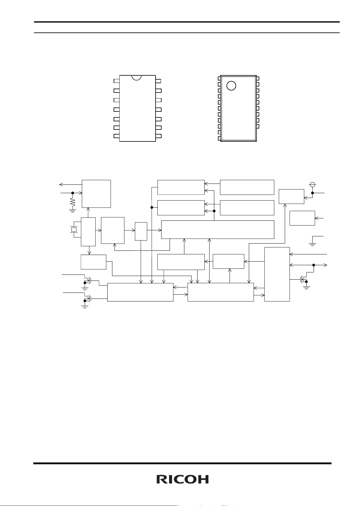
PIN CONFIGURATION
R2025S (SOP14)
R2025D (SON22)
N.C.
SCL SDA
32KOUT
N.C.
VPP
VDD N.C.
BLOCK DIAGRAM
32KOUT
CLKC
/INTRA
32kHz
OUTPUT
CONTROL
OSC
OSC
DETECT
DIVIDER
CORREC
-TION
1
2
3
4
5
6
7
TOP VIEW
DIV
N.C.
14
13
12
/INTRB
VSS
11
/INTRA
10
9
N.C.CLKC
8
COMPARATOR_W
COMPARATOR_D
(SEC,MIN,HOUR,WEEK,DAY,MONTH,YEAR)
ADDRESS
DECODER
CLKC
32KOUT
/INTRB
/INTRA
1
VDD
2
N.C. N.C.
3
VPP
4
5
SCL
6
SDA
7
8
VSS
9
10
N.C.
11
TOP VIEW
ALARM_W REGISTER
(MIN,HOUR, WEEK)
ALARM_D REGISTER
(MIN,HOUR)
TIME COUNTER
ADDRESS
REGISTER
22
21
20
19
18
17
16
15
14
N.C.
N.C.
N.C.
N.C.
N.C.
N.C.
N.C.
N.C.
I/O
CONTROL
VOLTAGE
DETECT
TEST
CIRCUIT
VDD
VPP
VSS
SCL
SDA
/INTRB
INTERRUPT CONTROL
SHIFT REGISTER
2

PIN DESCRIPTION
Symbol Item Description
SCL Serial
Clock Line
SDA Serial
Data Line
/INTRA Interrupt
Output A
/INTRB Interrupt
Output B
32KOUT 32K Clock
Output
CLKC Clock control
input
VDD
VSS
VPP Test input This pin is power pin for testing in the factory. Don’t connect to any lines.
N.C. No Connection These pins are not connected to internal IC chip.
Positive Power
Supply Input
Negative Power
Supply Input
The SCL pin is used to input clock pulses synchronizing the input and
output of data to and from the SDA pin. Allows a maximum input
voltage of 5.5 volts regardless of supply voltage.
The SDA pin is used to input or output data intended for writing or
reading in synchronization with the SCL pin. Up to 5.5v beyond VDD
may be input. This pin functions as an N-ch open drain output.
The /INTRA pin is used to output alarm interrupt (Alarm_D) and output
periodic interrupt signals to the CPU signals. Disabled at power-on
from 0V. N-ch. open drain output.
The /INTRA pin is used to output alarm interrupt (Alarm_W) and output
periodic interrupt signals to the CPU signals. Disabled at power-on
from 0V. N-ch. open drain output.
The 32KOUT pin is used to output 32.768-kHz clock pulses. Enabled
at power-on from 0 volts. CMOS output. The output is disabled and
held “L” when CLKC pi set to “L” or open, or certain register setting.
This pin is enabled at power-on from 0v.
The CLKC pin is used to control output of the 32KOUT pin. The clock
output is disabled and held low when the pin is set to low or open.
Incorporates a pull-down resistor.
The VDD pin is connected to the power supply.
The VSS pin is grounded.
In R2025D (SON22), N.C. pins from 14 pin to 22 pin are connected
together internally. Never connect these pins to any lines, or connect to
VDD or VSS. And never connect different voltage level lines each other.
R2025S/D
3
R2025S/D
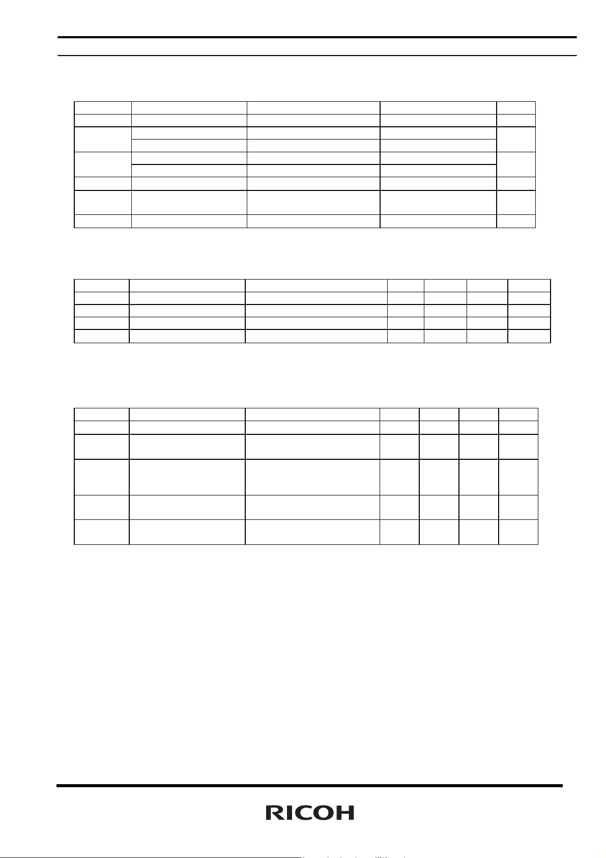
ABSOLUTE MAXIMUM RATINGS
(VSS=0V)
Symbol Item Pin Name and Condition Description Unit
VDD Supply Voltage VDD -0.3 to +6.5 V
Input Voltage 1 SCL, SDA, CLKC -0.3 to +6.5 VI
Input Voltage 2 VPP -0.3 to VDD+0.3
Output Voltage 1 SDA, /INTRA, /INTRB -0.3 to +6.5 VO
Output Voltage 2 32KOUT -0.3 to VDD+0.3
PD Power Dissipation
Topt Operating
Temperature
Tstg Storage Temperature -55 to +125
Topt=25°C
-40 to +85
300 mW
V
V
°C
°C
RECOMMENDED OPERATING CONDITION
(VSS=0V, Topt=-40 to +85°C)
Symbol Item Pin Name Min. Typ. Max. Unit
VDD Supply Voltage 1.7 5.5 V
VCLK Time Keeping Voltage 1.15 5.5 V
VPUP Pull-up Voltage SCL, SDA, /INTRA, /INTRB 5.5 V
RPUP Pull-up resister CLKC 10
kΩ
FREQUENCY CHARACTERISTICS
(VSS=0V)
Symbol Item Condition Min. Typ. Max. Unit
Δf/f0
Fv Frequency Voltage
Top Frequency
tsta Oscillation Start-up
fa Aging
Frequency Deviation
Characteristics
Temperature
Characteristics
Time
Topt=25°C, VDD=3V
Topt=25°C,
VDD=2.0V to 5.5V
Topt=-20°C to +70°C
25°C as standard
Topt=25°C, VDD=2V
Topt=25°C, VDD=3V,
First year
-5 0 +5 ppm
-1 +1 ppm
-120 +10 ppm
1 sec
-5 +5 ppm
4

R2025S/D
DC ELECTRICAL CHARACTERISTICS
Unless otherwise specified: VSS=0V,VDD=3V,Topt=-40 to +85°C
Symbol Item Pin Name Condition Min. Typ. Max. Unit
VIH “H” Input Voltage 0.8x
VIL “L” Input Voltage
IOH “H” Output
Current
IOL1 32KOUT 0.5
IOL2 /INTRA,
IOL3
IIL Input Leakage
ICLKC Pull-down
IOZ Output Off-state
IDD1
IDD2
VDETH
VDETL
“L” Output Current
Current
Resistance Input
Current
Leakage Current
Time Keeping
Current
Supply Voltage
Monitoring Voltage
(“H”)
Supply Voltage
Monitoring Voltage
(“L”)
SCL,SDA,
CLKC
32KOUT VOH=VDD-0.5V -0.5 mA
/INTRB
SDA
SCL VI=5.5V or VSS
CLKC VI=5.5V 0.3 1.0
SDA,
/INTRA
/INTRB
VDD
VDD
VDD
VDD
VDD=1.7 to 5.5V
VOL=0.4V
VDD=5.5V
VO=5.5V or VSS
VDD=5.5V
VDD=3V,
SCL=SDA=3V,
Output = OPEN
CLKC=”L”
VDD=5V,
SCL=SDA=5V,
Output = OPEN
CLKC=”L”
Topt=-30 to +70°C
Topt=-30 to +70°C
VDD
-0.3 0.2x
1.0
4.0
-1.0 1.0
-1.0
1.90
1.15
5.5
VDD
1.0
0.48 1.20
0.60 1.80
2.10 2.30
1.30 1.45
V
mA
μA
μA
μA
μA
μA
V
V
5
R2025S/D
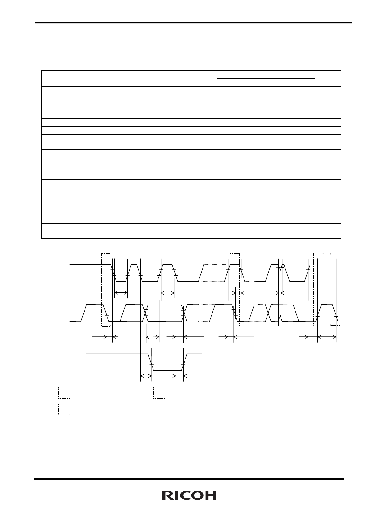
AC ELECTRICAL CHARACTERISTICS
Unless otherwise specified: VSS=0V,Topt=-40 TO +85°C
Input / Output condition: VIH=0.8xVDD,VIL=0.2xVDD,VOH=0.8xVDD,VOL=0.2xVDD,CL=50pF
Symbol Item Condi-
f
SCL
t
LOW
t
HIGH
t
HD;STA
t
SU;STO
t
SU;STA
t
RCV
tion
SCL Clock Frequency 400 KHz
SCL Clock ”L” Time 1.3
SCL Clock ”H” Time 0.6
Start Condition Hold Time 0.6
Stop Condition Set Up Time 0.6
Start Condition Set Up Time 0.6
Ricovery Time from Stop 62
Min. Typ. Max.
Condition to Start Condition
t
SU;DAT
t
HD;DAT
t
PL;DAT
Data Set Up Time 200 ns
Data Hold Time 0 ns
SDA “L” Stable Time
0.9
After Falling of SCL
t
PZ;DAT
SDA off Stable Time
0.9
After Falling of SCL
t
R
Rising Time of SCL and
300 ns
SDA (input)
t
F
Falling Time of SCL and
300 ns
SDA (input)
t
SP
Spike Width that can be
50 ns
removed with Input Filter
VDD≥1.7V
Unit
μs
μs
μs
μs
μs
μs
μs
μs
SCL
SDA(IN)
SDA(OUT)
S
Sr
S
t
LOW
t
PL;DAT
t
SU;DAT
t
HD;STA
Start Condition
Repeated Start Condition
t
RCV
S
Sr P
P
t
HIGH
t
HD;DAT
t
PZ;DAT
Stop Condition
t
HD;STA
t
SU;STA
tSP
t
SU;STO
6
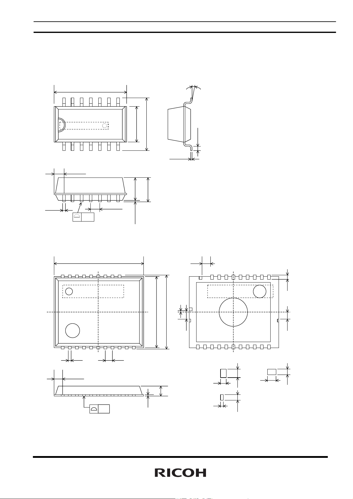
PACKAGE DIMENSIONS
#
#7 #1 #
A
#22
#14
#1
#
#1
#11
#22
#14
A
A’ B
A
• R2025S (SOP14)
1.24typ.
10.1±0.2
0.1
8
1.27±0.1
+0.1
5.0±0.2
3.1typ.
-0.05
0.1
7.4±0.2
0.1
±
3.2
14
+0.1
0.35
-0.05
• R2025D (SON22)
0°-10
0.15
°
+0.1
-0.05
R2025S/D
0.25
±
0.6
0.2
0.55typ.
±
6.1
0.2
0.65
0.1
±
0.3
5.0
0.05
B
0.43
0.2
±
0.1
B
’
0.3
0.3
0.43
0.2
0.1
0.2
0.2
0.2
±
±
4.7
±
0.1
0.5
11
±
0.1
1.3
+0.1/-0.05
0.125
0.1
7

R2025S/D
GENERAL DESCRIPTION
• Interface with CPU
The R2025S/D is connected to the CPU by two signal lines SCL and SDA, through which it reads and writes
data from and to the CPU. Since the output of the I/O pin of SDA is open drain, data interfacing with a CPU
different supply voltage is possible by applying pull-up resistors on the circuit board. The maximum clock frequency
of 400kHz (at VDD≥1.7V) of SCL enables data transfer in I
• Clock and Calendar Function
The R2025S/D reads and writes time data from and to the CPU in units ranging from seconds to the last two
digits of the calendar year. The calendar year will automatically be identified as a leap year when its last two digits
are a multiple of 4. Consequently, leap years up to the year 2099 can automatically be identified as such.
• Alarm Function
The R2025S/D incorporates the alarm interrupt circuit configured to generate interrupt signals to the CPU at
preset times. The alarm interrupt circuit allows two types of alarm settings specified by the Alarm_W registers and
the Alarm_D registers. The Alarm_W registers allow week, hour, and minute alarm settings including
combinations of multiple day-of-week settings such as "Monday, Wednesday, and Friday" and "Saturday and
Sunday". The Alarm_D registers allow hour and minute alarm settings. The Alarm_W outputs from /INTRB pin,
and the Alarm_D outputs from /INTRA pin. The current /INTRA or /INTRB conditions specified by the flag bits for
each alarm function can be checked from the CPU by using a polling function.
• High-precision Oscillation Adjustment Function
2
C-Bus fast mode.
To correct deviations in the oscillation frequency of the crystal oscillator, the oscillation adjustment circuit is
configured to allow correction of a time count gain or loss (up to ±1.5 ppm at 25°C) from the CPU within a
maximum range of approximately + 189 ppm in increments of approximately 3 ppm. Such oscillation frequency
adjustment in each system has the following advantages:
* Corrects seasonal frequency deviations through seasonal oscillation adjustment.
* Allows timekeeping with higher precision particularly with a temperature sensing function out of RTC,
through oscillation adjustment in tune with temperature fluctuations.
• Oscillation Halt Sensing Flag, Power-on Reset Flag, and Supply Voltage Monitoring Function
The R2025S/D incorporates an oscillation halt sensing circuit equipped with internal registers configured to
record any past oscillation halt.
Power-on reset flag is set to “1” When R2025S/D is powered on from 0V.
As such, the oscillation halt sensing flag and Power-on reset flag are useful for judging the validity of time data.
The R2025S/D also incorporates a supply voltage monitoring circuit equipped with internal registers configured
to record any drop in supply voltage below a certain threshold value. Supply voltage monitoring threshold settings
can be selected between 2.1 and 1.3 volts through internal register settings. The oscillation halt sensing circuit is
configured to confirm the established invalidation of time data in contrast to the supply voltage monitoring circuit
intended to confirm the potential invalidation of time data. Further, the supply voltage monitoring circuit can be
applied to battery supply voltage monitoring.
• Periodic Interrupt Function
The R2025S/D incorporates the periodic interrupt circuit configured to generate periodic interrupt signals aside
from interrupt signals generated by the periodic interrupt circuit for output from the /INTRA pin. Periodic interrupt
signals have five selectable frequency settings of 2 Hz (once per 0.5 seconds), 1 Hz (once per 1 second), 1/60 Hz
(once per 1 minute), 1/3600 Hz (once per 1 hour), and monthly (the first day of every month). Further, periodic
interrupt signals also have two selectable waveforms, a normal pulse form (with a frequency of 2 Hz or 1 Hz) and
8

R2025S/D
special form adapted to interruption from the CPU in the level mode (with second, minute, hour, and month
interrupts). The condition of periodic interrupt signals can be monitored by using a polling function.
• 32kHz Clock Output
The R2025S/D incorporates a 32-kHz clock output circuit configured to generate clock pulses with the oscillation
frequency of a 32.768kHz crystal oscillator for output from the 32KOUT pin (CMOS push-pull output). The 32-kHz
clock output is enabled and disabled when the CLKC pin is held high, and low or open, respectively. The 32-kHz
clock output can be disabled by certain register settings but cannot be disabled without manipulation of any two
registers with different addresses to prevent disabling in such events as the runaway of the CPU.
9
R2025S/D
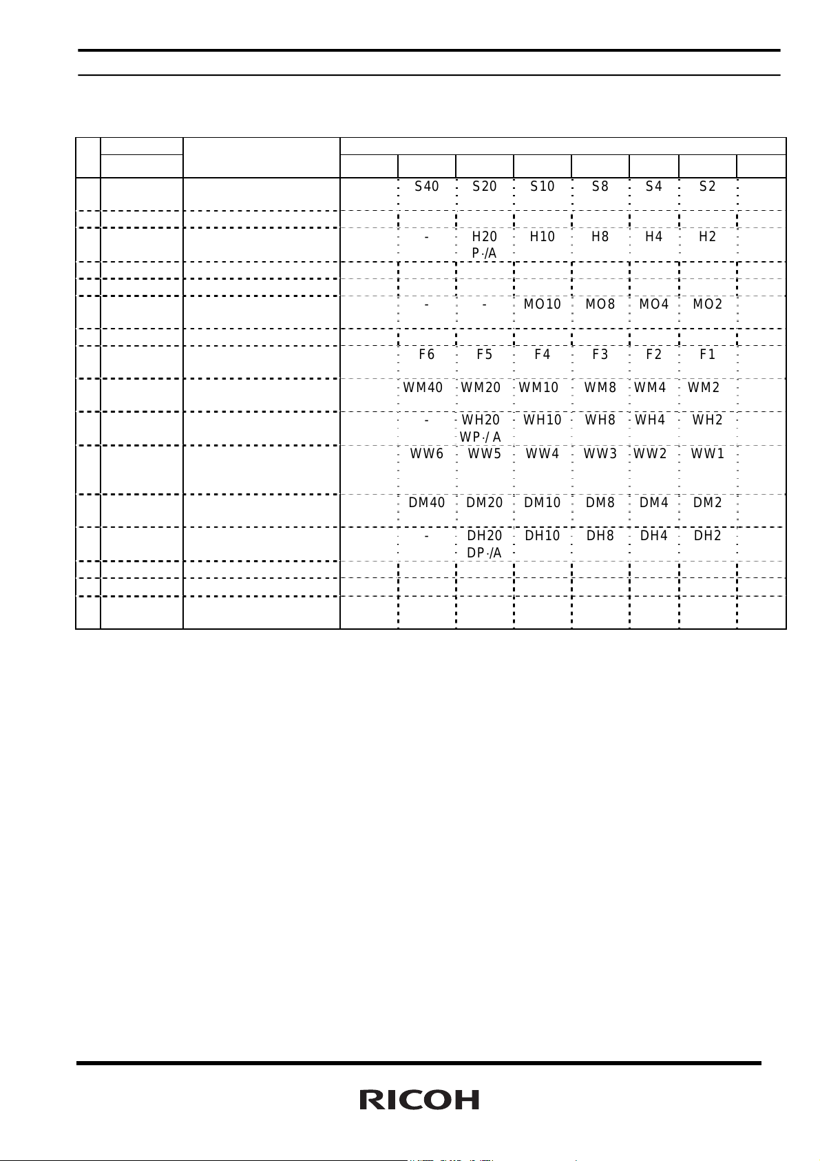
Address Mapping
Address Register Name D a t a
A3A2A1A0 D7 D6 D5 D4 D3 D2 D1 D0
0 0 0 0 0 Second Counter -
*2)
1 0 0 0 1 Minute Counter - M40 M20 M10 M8 M4 M2 M1
2 0 0 1 0 Hour Counter - - H20
3 0 0 1 1 Day-of-week Counter - - - - - W4 W2 W1
4 0 1 0 0 Day-of-month Counter - - D20 D10 D8 D4 D2 D1
5 0 1 0 1 Month Counter and
Century Bit
6 0 1 1 0 Year Counter Y80 Y40 Y20 Y10 Y8 Y4 Y2 Y1
7 0 1 1 1 Oscillation Adjustment
Register *3)
8 1 0 0 0 Alarm_W
(Minute Register)
9 1 0 0 1 Alarm_W
(Hour Register)
A 1 0 1 0 Alarm_W
(Day-of-week
Register)
B 1 0 1 1 Alarm_D
(Minute Register)
C 1 1 0 0 Alarm_D
(Hour Register)
D 1 1 0 1 - - - - - - - E 1 1 1 0 Control Register 1 *3) WALE DALE
F 1 1 1 1 Control Register 2 *3) VDSL VDET /XST PON
Notes:
*1) All the data listed above accept both reading and writing.
*2) The data marked with "-" is invalid for writing and reset to 0 for reading.
*3) When the PON bit is set to 1 in Control Register 2, all the bits are reset to 0 in Oscillation Adjustment
Register, Control Register 1 and Control Register 2 excluding the /XST and PON bits.
*4) The (0) bit should be set to 0.
*5) /XST is oscillation halt sensing bit.
*6) PON is power-on reset flag.
/19⋅20
(0)
*4)
- WM40 WM20 WM10 WM8 WM4 WM2 WM1
- - WH20
- WW6 WW5 WW4 WW3 WW2 WW1 WW0
- DM40 DM20 DM10 DM8 DM4 DM2 DM1
- - DH20
S40 S20 S10 S8 S4 S2 S1
H10 H8 H4 H2 H1
P⋅/A
- - MO10 MO8 MO4 MO2 MO1
F6 F5 F4 F3 F2 F1 F0
WH10 WH8 WH4 WH2 WH1
WP⋅/ A
DH10 DH8 DH4 DH2 DH1
DP⋅/A
/12⋅24
/CLEN2 TEST CT2 CT1 CT0
/CLEN1 CTFG WAFG DAFG
*5)
10
R2025S/D
Register Settings
• Control Register 1 (ADDRESS Eh)
D7 D6 D5 D4 D3 D2 D1 D0
WALE DALE
WALE DALE
0 0 0 0 0 0 0 0 Default Settings *)
*) Default settings: Default value means read / written values when the PON bit is set to “1” due to VDD
power-on from 0 volts.
/12⋅24
/12⋅24
(1) WALE, DALE Alarm_W Enable Bit, Alarm_D Enable Bit
WALE,DALE Description
0 Disabling the alarm interrupt circuit (under the control of the settings
of the Alarm_W registers and the Alarm_D registers).
1 Enabling the alarm interrupt circuit (under the control of the settings
of the Alarm_W registers and the Alarm_D registers)
(2) /12⋅24 /12-24-hour Mode Selection Bit
/12⋅24
0 Selecting the 12-hour mode with a.m. and p.m. indications. (Default)
1 Selecting the 24-hour mode
Setting the /12⋅24 bit to 0 and 1 specifies the 12-hour mode and the 24-hour mode, respectively.
24-hour mode 12-hour mode 24-hour mode 12-hour mode
00 12 (AM12) 12 32 (PM12)
01 01 (AM 1) 13 21 (PM 1)
02 02 (AM 2) 14 22 (PM 2)
03 03 (AM 3) 15 23 (PM 3)
04 04 (AM 4) 16 24 (PM 4)
05 05 (AM 5) 17 25 (PM 5)
06 06 (AM 6) 18 26 (PM 6)
07 07 (AM 7) 19 27 (PM 7)
08 08 (AM 8) 20 28 (PM 8)
09 09 (AM 9) 21 29 (PM 9)
10 10 (AM10) 22 30 (PM10)
11 11 (AM11) 23 31 (PM11)
Setting the /12⋅24 bit should precede writing time data
(3) /CLEN2 32-kHz Clock Output Bit2
/CLEN2 Description
0 Enabling the 32-kHz clock output (Default)
1 Disabling the 32-kHz clock output
Setting the /CLEN2 bit or the /CLEN1 bit (D3 in the control register 2) to 0 specifies generating clock pulses
with the oscillation frequency of the 32.768-kHz crystal oscillator for output from the 32KOUT pin.
Conversely, setting both the /CLEN1 and the /CLEN2 bit to 1 specifies disabling (“L”) such output.
(4) TEST Test Bit
TEST Description
0 Normal operation mode. (Default)
1 Test mode.
The TEST bit is used only for testing in the factory and should normally be set to 0.
/CLEN2 TEST CT2 CT1 CT0 (For Writing)
/CLEN2 TEST CT2 CT1 CT0 (For Reading)
(Default)
Description
11
R2025S/D
A
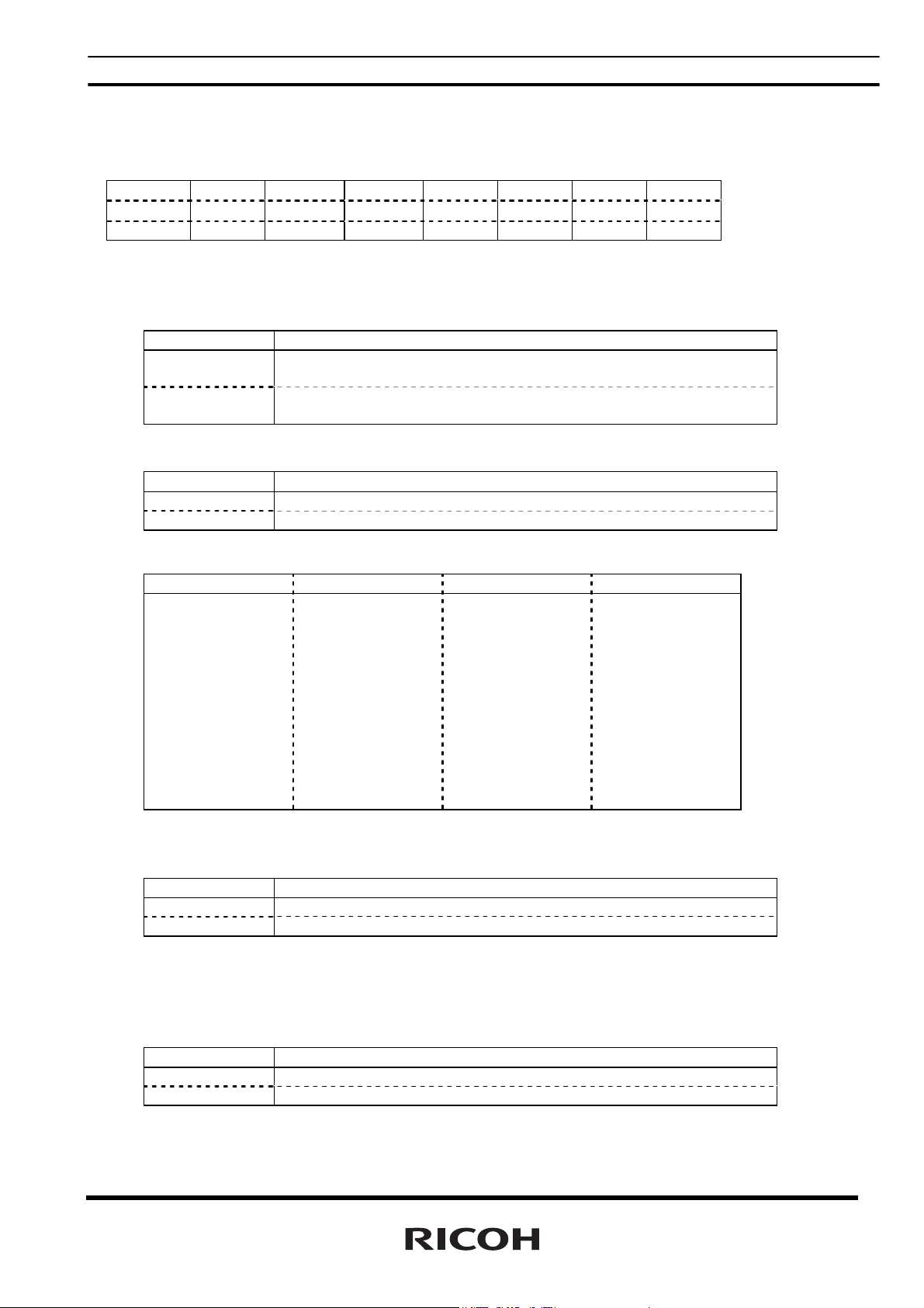
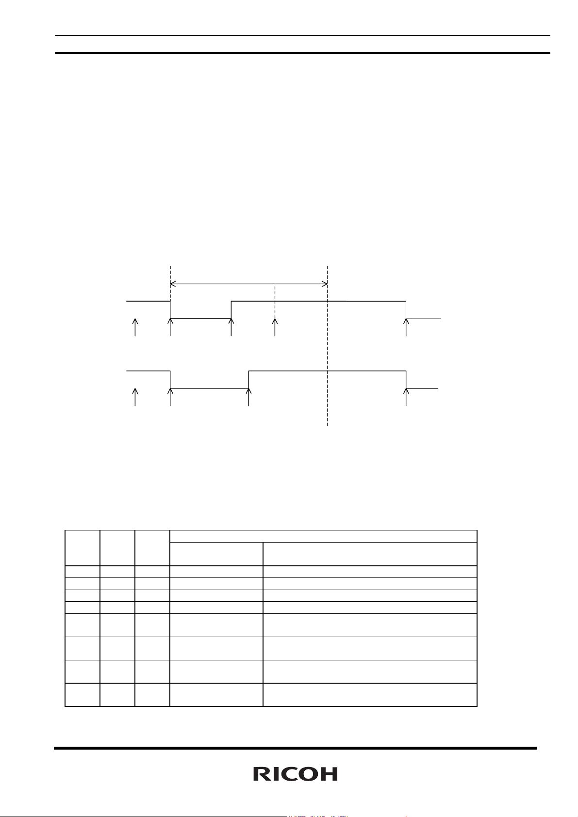
(5) CT2,CT1, and CT0 Periodic Interrupt Selection Bits
Description CT2 CT1 CT0
Wave form
mode
0 0 0 - OFF(H) (Default)
0 0 1 - Fixed at “L”
0 1 0 Pulse Mode
*1)
0 1 1 Pulse Mode
*1)
1 0 0 Level Mode
*2)
1 0 1 Level Mode
*2)
1 1 0 Level Mode
*2)
1 1 1 Level Mode
*2)
* 1) Pulse Mode: 2-Hz and 1-Hz clock pulses are output in synchronization with the increment of the second
counter as illustrated in the timing chart below.
Interrupt Cycle and Falling Timing
2Hz(Duty50%)
1Hz(Duty50%)
Once per 1 second (Synchronized with
second counter increment)
Once per 1 minute (at 00 seconds of
every minute)
Once per hour (at 00 minutes and 00
seconds of every hour)
Once per month (at 00 hours, 00
minutes,
and 00 seconds of first day of every
month)
CTFG Bi t
/INTRA Pin
pprox. 92μs
(Increment of second counter)
Rewriting of the second counter
In the pulse mode, the increment of the second counter is delayed by approximately 92 μs from the falling
edge of clock pulses. Consequently, time readings immediately after the falling edge of clock pulses may
appear to lag behind the time counts of the real-time clocks by approximately 1 second. Rewriting the
second counter will reset the other time counters of less than 1 second, driving the /INTRA pin low.
* 2) Level Mode: Periodic interrupt signals are output with selectable interrupt cycle settings of 1 second, 1
minute, 1 hour, and 1 month. The increment of the second counter is synchronized with the falling edge of
periodic interrupt signals. For example, periodic interrupt signals with an interrupt cycle setting of 1 second
are output in synchronization with the increment of the second counter as illustrated in the timing chart below.
CTFG Bit
/INTRA Pin
Setting CTFG bit to 0
(Increment of
second counter)
(Increment of
second counter)
Setting CTFG bit to 0
(Increment of
second counter)
12
R2025S/D
*1), *2) When the oscillation adjustment circuit is used, the interrupt cycle will fluctuate once per 20sec. or
60sec. as follows:
Pulse Mode: The “L” period of output pulses will increment or decrement by a maximum of ±3.784 ms. For
example, 1-Hz clock pulses will have a duty cycle of 50 ±0.3784%.
Level Mode: A periodic interrupt cycle of 1 second will increment or decrement by a maximum of ±3.784 ms.
• Control Register 2 (Address Fh)
D7 D6 D5 D4 D3 D2 D1 D0
VDSL VDET /XST PON /CLE
N1
VDSL VDET /XST PON /CLE
N1
0 0
*) Default settings: Default value means read / written values when the PON bit is set to “1” due to VDD
power-on from 0 volts.
Indefinit
e
1 0 0 0 0 Default Settings *)
(1) VDSL VDD Supply Voltage Monitoring Threshold Selection Bit
VDSL Description
0 Selecting the VDD supply voltage monitoring threshold setting of
2.1v.
1 Selecting the VDD supply voltage monitoring threshold setting of
1.3v.
The VDSL bit is intended to select the VDD supply voltage monitoring threshold settings.
(2) VDET Supply Voltage Monitoring Result Indication Bit
VDET Description
0 Indicating supply voltage above the supply voltage monitoring
threshold settings.
1 Indicating supply voltage below the supply voltage monitoring
threshold settings.
Once the VDET bit is set to 1, the supply voltage monitoring circuit will be disabled while the VDET bit will
hold the setting of 1. The VDET bit accepts only the writing of 0, which restarts the supply voltage
monitoring circuit. Conversely, setting the VDET bit to 1 causes no event.
(3) /XST Oscillation Halt Sensing Monitor Bit
/XST Description
0 Sensing a halt of oscillation
1 Sensing a normal condition of oscillation
The /XST accepts the reading and writing of 0 and 1. The /XST bit will be set to 0 when the oscillation halt
sensing. The /XST bit will hold 0 even after the restart of oscillation.
(4) PON Power-on-reset Flag Bit
PON Description
0 Normal condition
1 Detecting VDD power-on -reset (Default)
The PON bit is for sensing power-on reset condition.
* The PON bit will be set to 1 when VDD power-on from 0 volts. The PON bit will hold the setting of 1 even
after power-on.
* When the PON bit is set to 1, all bits will be reset to 0, in the Oscillation Adjustment Register, Control
Register 1, and Control Register 2, except /XST and PON. As a result, /INTRA and /INTRB pins stop
outputting.
* The PON bit accepts only the writing of 0. Conversely, setting the PON bit to 1 causes no event.
CTFG WAF
G
CTFG WAF
G
DAFG (For Writing)
DAFG (For Reading)
(Default)
(Default)
13
R2025S/D
A
A
(5) /CLEN1 32-kHz Clock Output Bit 1
/CLEN1 Description
0 Enabling the 32-kHz clock output (Default)
1 Disabling the 32-kHz clock output
Setting the /CLEN1 bit or the /CLEN2 bit (D4 in the control register 1) to 0 specifies generating clock pulses
with the oscillation frequency of the 32.768-kHz crystal oscillator for output from the 32KOUT pin.
Conversely, setting both the /CLEN1 and the /CLEN2 bit to 1 specifies disabling (“L”) such output.
(6) CTFG Periodic Interrupt Flag Bit
CTFG Description
0 Periodic interrupt output = “H” (Default)
1 Periodic interrupt output = “L”
The CTFG bit is set to 1 when the periodic interrupt signals are output from the /INTRA pin (“L”). The
CTFG bit accepts only the writing of 0 in the level mode, which disables (“H”) the /INTRA pin until it is
enabled (“L”) again in the next interrupt cycle. Conversely, setting the CTFG bit to 1 causes no event.
(7) WAFG,DAFG Alarm_W Flag Bit and Alarm_D Flag Bit
WAFG,DAFG Description
0 Indicating a mismatch between current time and preset alarm time (Default)
1 Indicating a match between current time and preset alarm time
The WAFG and DAFG bits are valid only when the WALE and DALE have the setting of 1, which is caused
approximately 61μs after any match between current time and preset alarm time specified by the Alarm_W
registers and the Alarm_D registers. The WAFG (DAFG) bit accepts only the writing of 0. /INTRB
(/INTRA) pin outputs off (“H”) when this bit is set to 0. And /INTRB (/INTRA) pin outputs “L” again at the
next preset alarm time. Conversely, setting the WAFG and DAFG bits to 1 causes no event. The WAFG
and DAFG bits will have the reading of 0 when the alarm interrupt circuit is disabled with the WALE and
DALE bits set to 0. The settings of the WAFG (DAFG) bit is synchronized with the output of the
/INTRB (/INTRA) pin as shown in the timing chart below.
pprox. 61μs
pprox. 61μs
WAFG(DAFG) Bit
/INTRB(/INTRA) Pin
Writing of 0 to
WAFG(DAFG) bit
(Match between
current time and
preset alarm time)
(Match between
current time and
preset alarm time)
(Match between
current time and
preset alarm time)
Writing of 0 to
WAFG(DAFG) bit
14
R2025S/D
• Time Counter (Address 0-2h)
Second Counter (Address 0h)
D7 D6 D5 D4 D3 D2 D1 D0
- S40 S20 S10 S8 S4 S2 S1 (For Writing)
0 S40 S20 S10 S8 S4 S2 S1 (For Reading)
0
Minute Counter (Address 1h)
D7 D6 D5 D4 D3 D2 D1 D0
- M40 M20 M10 M8 M4 M2 M1 (For Writing)
0 M40 M20 M10 M8 M4 M2 M1 (For Reading)
0
Hour Counter (Address 2h)
D7 D6 D5 D4 D3 D2 D1 D0
- -
0 0
0 0
*) Default settings: Default value means read / written values when the PON bit is set to “1” due to VDD
power-on from 0 volts.
* Time digit display (BCD format) as follows:
The second digits range from 00 to 59 and are carried to the minute digit in transition from 59 to 00.
The minute digits range from 00 to 59 and are carried to the hour digits in transition from 59 to 00.
The hour digits range as shown in "P
Selection Bit" and are carried to the day-of-month and day-of-week digits in transition from PM11 to AM12
or from 23 to 00.
* Any writing to the second counter resets divider units of less than 1 second.
* Any carry from lower digits with the writing of non-existent time may cause the time counters to malfunction.
Therefore, such incorrect writing should be replaced with the writing of existent time data.
Indefinite Indefinite Indefinite Indefinite Indefinite Indefinite Indefinite
Indefinite Indefinite Indefinite Indefinite Indefinite Indefinite Indefinite
P⋅/A
or
H20
P⋅/A
or
H20
Indefinite Indefinite Indefinite Indefinite Indefinite Indefinite
H10 H8 H4 H2 H1 (For Writing)
H10 H8 H4 H2 H1 (For Reading)
11 • Control Register 1 (ADDRESS Eh) (2) /12⋅24: /12-24-hour Mode
Default Settings *)
Default Settings *)
Default Settings *)
• Day-of-week Counter (Address 3h)
D7 D6 D5 D4 D3 D2 D1 D0
- - - - - W4 W2 W1 (For Writing)
0 0 0 0 0 W4 W2 W1 (For Reading)
0 0 0 0 0
*) Default settings: Default value means read / written values when the PON bit is set to “1” due to VDD
power-on from 0 volts.
* The day-of-week counter is incremented by 1 when the day-of-week digits are carried to the day-of-month
digits.
* Day-of-week display (incremented in septimal notation):
(W4, W2, W1) = (0, 0, 0) → (0, 0, 1)→…→(1, 1, 0) → (0, 0, 0)
* Correspondences between days of the week and the day-of-week digits are user-definable
(e.g. Sunday = 0, 0, 0)
* The writing of (1, 1, 1) to (W4, W2, W1) is prohibited except when days of the week are unused.
Indefinite Indefinite Indefinite
Default Settings *)
15

R2025S/D
• Calendar Counter (Address 4-6h)
Day-of-month Counter (Address 4h)
D7 D6 D5 D4 D3 D2 D1 D0
- - D20 D10 D8 D4 D2 D1 (For Writing)
0 0 D20 D10 D8 D4 D2 D1 (For Reading)
0 0
Month Counter + Century Bit (Address 5h)
D7 D6 D5 D4 D3 D2 D1 D0
/19⋅20
/19⋅20
Indefinite
Year Counter (Address 6h)
D7 D6 D5 D4 D3 D2 D1 D0
Y80 Y40 Y20 Y10 Y8 Y4 Y2 Y1 (For Writing)
Y80 Y40 Y20 Y10 Y8 Y4 Y2 Y1 (For Reading)
Indefinite Indefinite Indefinite Indefinite Indefinite Indefinite Indefinite Indefinite
*) Default settings: Default value means read / written values when the PON bit is set to “1” due to VDD
power-on from 0 volts.
* The calendar counters are configured to display the calendar digits in BCD format by using the automatic
calendar function as follows:
The day-of-month digits (D20 to D1) range from 1 to 31 for January, March, May, July, August, October, and
December; from 1 to 30 for April, June, September, and November; from 1 to 29 for February in leap years;
from 1 to 28 for February in ordinary years. The day-of-month digits are carried to the month digits in
reversion from the last day of the month to 1. The month digits (MO10 to MO1) range from 1 to 12 and are
carried to the year digits in reversion from 12 to 1.
The year digits (Y80 to Y1) range from 00 to 99 (00, 04, 08, …, 92, and 96 in leap years) and are carried to
the /19⋅20 digits in reversion from 99 to 00.
The /19⋅20 digits cycle between 0 and 1 in reversion from 99 to 00 in the year digits.
* Any carry from lower digits with the writing of non-existent calendar data may cause the calendar counters
to malfunction. Therefore, such incorrect writing should be replaced with the writing of existent calendar
data.
- - MO10 MO8 MO4 MO2 MO1 (For Writing)
0 0 MO10 MO8 MO4 MO2 MO1 (For Reading)
0 0
Indefinite Indefinite Indefinite Indefinite Indefinite Indefinite
Indefinite Indefinite Indefinite Indefinite Indefinite
Default Settings *)
Default Settings *)
Default Settings *)
• Oscillation Adjustment Register (Address 7h)
16
D7 D6 D5 D4 D3 D2 D1 D0
(0) F6 F5 F4 F3 F2 F1 F0 (For Writing)
0 F6 F5 F4 F3 F2 F1 F0 (For Reading)
0 0 0 0 0 0 0 0 Default Settings *)
*) Default settings: Default value means read / written values when the PON bit is set to “1” due to VDD
power-on from 0 volts.
(0) bit:
(0) bit should be set to 0
F6 to F0 bits:
* The Oscillation Adjustment Circuit is configured to change time counts of 1 second on the basis of the
settings of the Oscillation Adjustment Register when the second digits read 00, 20, or 40 seconds. Normally,

R2025S/D
the Second Counter is incremented once per 32768 32.768-kHz clock pulses generated by the crystal
oscillator. Writing to the F6 to F0 bits activates the oscillation adjustment circuit.
* The Oscillation Adjustment Circuit will not operate with the same timing (00, 20, or 40 seconds)
as the timing of writing to the Oscillation Adjustment Register.
* The F6 bit setting of 0 causes an increment of time counts by ((F5, F4, F3, F2, F1, F0) - 1) x 2.
The F6 bit setting of 1 causes a decrement of time counts by ((/F5, /F4, /F3, /F2, /F1, /F0) + 1) x 2.
The settings of "*, 0, 0, 0, 0, 0, *" ("*" representing either "0" or "1") in the F6, F5, F4, F3, F2, F1, and F0 bits
cause neither an increment nor decrement of time counts.
Example:
When the second digits read 00, 20, or 40, the settings of "0, 0, 0, 0, 1, 1, 1" in the F6, F5, F4, F3, F2, F1, and
F0 bits cause an increment of the current time counts of 32768 by (7 - 1) x 2 to 32780 (a current time count
loss). When the second digits read 00, 20, or 40, the settings of "0, 0, 0, 0, 0, 0, 1" in the F6, F5, F4, F3, F2,
F1, and F0 bits cause neither an increment nor a decrement of the current time counts of 32768.
When the second digits read 00, 20, or 40, the settings of "1, 1, 1, 1, 1, 1, 0" in the F6, F5, F4, F3, F2, F1, and
F0 bits cause a decrement of the current time counts of 32768 by (- 2) x 2 to 32764 (a current time count
gain).
An increase of two clock pulses once per 20 seconds causes a time count loss of approximately 3 ppm (2 /
(32768 x 20 = 3.051 ppm). Conversely, a decrease of two clock pulses once per 20 seconds causes a time
count gain of 3 ppm. Consequently, deviations in time counts can be corrected with a precision of ±1.5 ppm.
Note that the oscillation adjustment circuit is configured to correct deviations in time counts and not the
oscillation frequency of the 32.768-kHz clock pulses. For further details, see "P
Oscillation Circuit and Correction of Time Count Deviations • Oscillation Adjustment Circuit".
28 Configuration of
17

R2025S/D
• Alarm_W Registers (Address 8-Ah)
Alarm_W Minute Register (Address 8h)
D7 D6 D5 D4 D3 D2 D1 D0
- WM40 WM20 WM10 WM8 WM4 WM2 WM1 (For Writing)
0 WM40 WM20 WM10 WM8 WM4 WM2 WM1 (For Reading)
0
Alarm_W Hour Register (Address 9h)
D7 D6 D5 D4 D3 D2 D1 D0
- - WH20
0 0 WH20
0 0
Alarm_W Day-of-week Register (Address Ah)
D7 D6 D5 D4 D3 D2 D1 D0
- WW6 WW5 WW4 WW3 WW2 WW1 WW0 (For Writing)
0 WW6 WW5 WW4 WW3 WW2 WW1 WW0 (For Reading)
0
*) Default settings: Default value means read / written values when the PON bit is set to “1” due to VDD
power-on from 0 volts.
* The D5 bit of the Alarm_W Hour Register represents WP/A when the 12-hour mode is selected (0 for a.m.
and 1 for p.m.) and WH20 when the 24-hour mode is selected (tens in the hour digits).
* The Alarm_W Registers should not have any non-existent alarm time settings.
(Note that any mismatch between current time and preset alarm time specified by the Alarm_W registers may
disable the alarm interrupt circuit.)
* When the 12-hour mode is selected, the hour digits read 12 and 32 for 0 a.m. and 0 p.m., respectively. (See
"P
11 •Control Register 1 (ADDRESS Eh) (2) /12⋅24: 12-/24-hour Mode Selection Bit")
* WW0 to WW6 correspond to W4, W2, and W1 of the day-of-week counter with settings ranging from (0, 0,
0) to (1, 1, 0).
* WW0 to WW6 with respective settings of 0 disable the outputs of the Alarm_W Registers.
Indefinite Indefinite Indefinite Indefinite Indefinite Indefinite Indefinite
WH10 WH8 WH4 WH2 WH1 (For Writing)
WP⋅/A
WH10 WH8 WH4 WH2 WH1 (For Reading)
WP⋅/A
Indefinite Indefinite Indefinite Indefinite Indefinite Indefinite
Indefinite Indefinite Indefinite Indefinite Indefinite Indefinite Indefinite
Default Settings *)
Default Settings *)
Default Settings *)
18

R2025S/D
Example of Alarm Time Setting
Alarm Day-of-week 12-hour mode 24-hour mode
Preset alarm time Sun. Mon. Tue. Wed. Th. Fri. Sat. 1
00:00 a.m. on all
WW0 WW1 WW2 WW3 WW4 WW5 WW6
1 1 1 1 1 1 1 1 2 0 0 0 0 0 0
1
1
1
1
1
1
h
0
h
r
r.
.
m
in
0
m
in
.
.
0
h
r
.
h
0
m
r.
in
.
days
01:30 a.m. on all
1 1 1 1 1 1 1 0 1 3 0 0 1 3 0
days
11:59 a.m. on all
1 1 1 1 1 1 1 1 1 5 9 1 1 5 9
days
00:00 p.m. on Mon.
0 1 1 1 1 1 0 3 2 0 0 1 2 0 0
to Fri.
01:30 p.m. on Sun. 1 0 0 0 0 0 0 2 1 3 0 1 3 3 0
11:59 p.m.
0 1 0 1 0 1 0 3 1 5 9 2 3 5 9
on Mon. ,Wed.,
and Fri.
Note that the correspondence between WW0 to WW6 and the days of the week shown in the above table is
only an example and not mandatory.
• Alarm_D Register (Address B-Ch)
1
mi
n.
Alarm_D Minute Register (Address Bh)
D7 D6 D5 D4 D3 D2 D1 D0
- DM40 DM20 DM10 DM8 DM4 DM2 DM1 (For Writing)
0 DM40 DM20 DM10 DM8 DM4 DM2 DM1 (For Reading)
0
Indefinite Indefinite Indefinite Indefinite Indefinite Indefinite Indefinite
Default Settings *)
Alarm_D Hour Register (Address Ch)
D7 D6 D5 D4 D3 D2 D1 D0
- - DH20
DH10 DH8 DH4 DH2 DH1 (For Writing)
DP⋅/A
0 0 DH20
DH10 DH8 DH4 DH2 DH1 (For Reading)
DP⋅/A
0 0
Indefinite Indefinite Indefinite Indefinite Indefinite Indefinite
Default Settings *)
*) Default settings: Default value means read / written values when the PON bit is set to “1” due to VDD
power-on from 0 volts.
* The D5 bit represents DP/A when the 12-hour mode is selected (0 for a.m. and 1 for p.m.) and DH20 when
the 24-hour mode is selected (tens in the hour digits).
* The Alarm_D registers should not have any non-existent alarm time settings.
(Note that any mismatch between current time and preset alarm time specified by the Alarm_D registers
may disable the alarm interrupt circuit.)
* When the 12-hour mode is selected, the hour digits read 12 and 32 for 0a.m. and 0p.m., respectively.
(See "P
11 •Control Register 1 (ADDRESS Eh) (2) /12⋅24: 12-/24-hour Mode Selection Bit")
19

R2025S/D
Interfacing with the CPU
The R2025S/D employs the I2C-Bus system to be connected to the CPU via 2-wires. Connection and system of
2
I
C-Bus are described in the following sections.
Connection of I2C-Bus
2-wires, SCL and SDA pins that are connected to I2C-Bus are used for transmit clock pulses and data
respectively. All ICs that are connected to these lines are designed that will not be clamped when a voltage
beyond supply voltage is applied to input or output pins. Open drain pins are used for output. This construction
allows communication of signals between ICs with different supply voltages by adding a pull-up resistor to each
signal line as shown in the figure below. Each IC is designed not to affect SCL and SDA signal lines when power
to each of these is turned off separately.
VDD1
VDD2
VDD3
VDD4
Rp Rp
SCL
SDA
* For data interface, the following
conditions must be met:
VCC4≥VCC1
VCC4≥VCC2
VCC4≥VCC3
* When the master is one, the
micro-controller is ready for driving
SCL to “H” and Rp of SCL may not be
required.
Micro-
Controller
R2025S/D
Other
Peripheral
Device
Cautions on determining Rp resistance,
(1) Dropping voltage at Rp due to sum of input current or output current at off conditions on each IC pin
connected to the I
2
C-Bus shall be adequately small.
(2) Rising time of each signal be kept short even when all capacity of the bus is driven.
(3) Current consumed in I
2
C-Bus is small compared to the consumption current permitted for the entire system.
When all ICs connected to I
2
C-Bus are CMOS type, condition (1) may usually be ignored since input current and
off-state output current is extremely small for the many CMOS type ICs. Thus the maximum resistance of Rp may
be determined based on (2), while the minimum on (3) in most cases. In actual cases a resistor may be place
between the bus and input/output pins of each IC to improve noise margins in which case the Rp minimum value
may be determined by the resistance. Consumption current in the bus to review (3) above may be expressed by
the formula below:
Bus consumption current ≈
(Sum of input current and off state output current of all devices in standby mode ) × Bus standby duration
Bus stand-by duration + the Bus operation duration
+
Supply voltage × Bus operation duration × 2
Rp resistance × 2 × (Bus stand-by duration + bus operation duration)
+ Supply voltage × Bus capacity × Charging/Discharging times per unit time
Operation of “× 2” in the second member denominator in the above formula is derived from assumption that “L”
20

R2025S/D
duration of SDA and SCL pins are the half of bus operation duration. “× 2” in the numerator of the same member
is because there are two pins of SDA and SCL. The third member, (charging/discharging times per unit time)
means number of transition from “H” to “L” of the signal line.
Calculation example is shown below:
Pull-up resistor (Rp) = 10kΩ, Bus capacity = 50pF(both for SCL, SDA), VDD=3v,
In a system with sum of input current and off-state output current of each pin = 0.1μA,
2
I
C-Bus is used for 10ms every second while the rest of 990ms in the stand-by mode,
In this mode, number of transitions of the SCL pin from “H” to “L” state is 100 while SDA 50, every second.
Bus consumption current ≈
990msec + 10msec
+
10KΩ × 2 × (990msec + 10msec)
+ 3V × 50pF × (100 + 50)
≈ 0.099μA + 3.0μA + 0.0225μA ≈ 3.12μA
Generally, the second member of the above formula is larger enough than the first and the third members bus
consumption current may be determined by the second member is many cases.
• Transmission System of I
0.1μA×990msec
3V × 10msec × 2
2
C-Bus
(1) Start Condition and Stop Condition
In I2C-Bus, SDA must be kept at a certain state while SCL is at the “H” state during data transmission as shown
below.
SCL
SDA
tSU;DAT
The SCL and SDA pins are at the “H” level when no data transmission is made. Changing the SDA from “H” to
“L” when the SCL and the SDA are “H” activates the Start Condition and access is started. Changing the SDA from
“L” to “H” when the SCL is “H” activates Stop Condition and accessing stopped. Generation of Start and Stop
Conditions are always made by the master (see the figure below).
tHD;DAT
21

R2025S/D
SCL
SDA
Start Condition Stop Condition
tHD;STA tSU;STO
(2) Data transmission and its acknowledge
After Start condition is entered, data is transmitted by 1byte (8bits). Any bytes of data may be serially
transmitted. The receiving side will send an acknowledge signal to the transmission side each time 8bit data is
transmitted. The acknowledge signal is sent immediately after falling to “L” of SCL 8bit clock pulses of data is
transmitted, by releasing the SDA by the transmission side that has asserted the bus at that time and by turning
SDA to “L” by receiving side. When transmission of 1byte data next to preceding 1byte of data is received the
receiving side releases the SDA pin at falling edge of the SCL 9bit of clock pulses or when the receiving side
switches to the transmission side it starts data transmission. When the master is receiving side, it generates no
acknowledge signal after last 1byte of data from the slave to tell the transmitter that data transmission has
completed. The slave side (transmission side) continues to release the SDA pin so that the master will be able to
generate Stop Condition, after falling edge of the SCL 9bit of clock pulses.
SCL
from the master
SDA from
the transmission side
SDA from
the receiving side
Start
Condition
12 89
Acknowledge
signal
22

R2025S/D
A
(3) Data Transmission Format in I2C-Bus
I2C-Bus has no chip enable signal line. In place of it, each device has a 7bit Slave Address allocated. The first
1byte is allocated to this 7bit address and to the command (R/W) for which data transmission direction is
designated by the data transmission thereafter. 7bit addr ess is sequentially transmitted from the MSB and 2 and
after bytes are read, when 8bit is “H” and when write “L”.
The Slave Address of the R2025S/D is specified at (0110010).
At the end of data transmission / receiving, Stop Condition is generated to complete transmission. However, if
start condition is generated without generating Stop Condition, Repeated Start Condition is met and transmission /
receiving data may be continue by setting the Slave Address again. Use this procedure when the transmission
direction needs to be change during one transmission.
Data is written to the slave
from the master
When data is read from the
slave immediately after 7bit
addressing from the master
Slave Address Data
S 0 A
Slave Address
S 1 A /A P
(0110010)
A A P
R/W=0(Write)(0110010)
A
R/W=1(Read)
Data
Data
Data
Inform read has been completed b y not g ener ate
an acknowledge signal to the slave side.
When the transmission
direction is to be changed
during transmission.
Master to slave Slave to master
Start Condition
S
Slave Address
S
(0110010)
Data
R/W=0(Write)
Stop Condition
P
Data
AA
Inform read has been com pleted b y not generate
an acknowledge signal to the slave side.
Data
/A P
A A /A
Sr
Salve Address
Sr 10 AA
cknowledge Signal
Repeated Start Condition
R/W=1(Read)(0110010)
23

R2025S/D
A
(4) Data Transmission Write Format in the R2025S/D
Although the I2C-Bus standard defines a transmission format for the slave allocated for each IC, transmission
method of address information in IC is not defined. The R2025S/D transmits data the internal address pointer
(4bit) and the Transmission Format Register (4bit) at the 1byte next to one which transmitted a Slave Address and
a write command. For write operation only one transmission format is available and (0000) is set to the
Transmission Format Register. The 3byte transmits data to the address specified by the internal address pointer
written to the 2byte. Internal address pointer setting are automatically incremented for 4byte and after. Note that
when the internal address pointer is Fh, it will change to 0h on transmitting the next byte.
Example of data writing (When writing to internal address Eh to Fh)
R/W=0(Write)
1 AS 0 A
Slave Address
←(0110010)
S
A A /A
A
110 0 00 0 0 0 00 1 11
Address
Pointer
←Eh
Master to slave Slave to master
Start Condition
Transmission
Format
Register
0h
cknowledge signal
Data
Writing of data to the
internal address Eh
←
Stop Condition
P
Writing of data to the
internal address Fh
Data
A P
(5) Data transmission read format of the R2025S/D
The R2025S/D allows the following three read out method of data an internal register.
The first method to reading data from the internal register is to specify an internal address by setting the internal
address pointer and the transmission format register described P
(See P
23 (3)) to change the data transmission direction to perform reading. The internal address pointer is set to
Fh when the Stop Condition is met. Therefore, this method of reading allows no insertion of Stop Condition before
the Repeated Start Condition. Set 0h to the Transmission Format Register when this method used.
24 (4), generate the Repeated Start Condition
24

Example 1 of Data Read (when data is read from 2h to 4h)
A
A
R2025S/D
R/W=0(Write)
S 0A A
Slave Address
← (0110010)
S
A A /A
1 0 0 0 0 1
Reading of data from
the internal address 2h
Master to slave
Start Condition
0 10 00 11 0 0 0 00 0 1
Address
Pointer
←2h
Data
cknowledge signal
Repeated Start Condition
Sr1 0 A
Transmission
Format
Register←0h
A
Reading of data from
the internal address 3h
Data
Slave to master
Repeated Start
Sr
Condition
1
Slave Address
← (0110010)
A
R/W=1(Read)
Data
Reading of data from
the internal address 4h
P
Stop Condition
/A P
The second method to reading data from the internal register is to start reading immediately after writing to the
Internal Address Pointer and the Transmission Format Register. Although this method is not based on I
2
C-Bus
standard in a strict sense it still effective to shorten read time to ease load to the master. Set 4h to the transmission
format register when this method used.
Example 2 of data read (when data is read from internal addresses Eh to 1h)
1 0 A
Slave Address
(0110010)
←
Master to slave Slave to Master
Start Condition
S
A A /A
R/W=0(Write)
10 0 00 1
Data
Reading of data from
the internal address Fh
cknowledge Signal
1S A A
Address
Pointer
Eh
←
0 11 0 001
Transmission
Format
Register←4h
A
Reading of data from
the internal address 0h
Reading of data from
the internal address Eh
Data
Stop Condition
P
Data
A
Reading of data from
the internal address 1h
Data
/A P
25
R2025S/D
A
The third method to reading data from the internal register is to start reading immediately after writing to the
Slave Address and R/W bit. Since the Internal Address Pointer is set to Fh by default as described in the first
method, this method is only effective when reading is started from the Internal Address Fh.
Example 3 of data read (when data is read from internal addresses Fh to 3h)
R/W=1(Re ad)
S A A
1 0 A
Slave Address
← (0110010)
S
A A /A
10 0 10 1
Reading of data from
the Internal Address Fh
Data
Reading of data from
the Internal Address 1h
Master to slave Slav e to m aster
Start Conditi on
cknowledge Signal
Data
Reading of data from
the Internal Address 0h
A
Reading of data from
the Internal Address 2h
Data
Stop Condition
P
Data
A
Reading of data from
the Internal Address 3h
Data
/A P
26

R2025S/D
Data Transmission under Special Condition
The R2025S/D holds the clock tentatively for duration from Start Condition to avoid invalid read or write clock on
carrying clock. When clock carried during this period, which will be adjusted within approx. 61μs from Stop
Condition. To prevent invalid read or write, clock and calendar data shall be made during one transmission
operation (from Start Condition to Stop Condition). When 0.5 to 1.0 second elapses after Start Condition, any
access to the R2025S/D is automatically released to release tentative hold of the clock, and access from the CPU
is forced to be terminated (The same action as made Stop Condition is received: automatic resume function from
I2C-Bus interface). Therefore, one access must be complete within 0.5 seconds. The automatic resume
function prevents delay in clock even if SCL is stopped from sudden failure of the system during clock read
operation.
Also a second Start Condition after the first Start Condition and before the Stop Condition is regarded “Repeated
Start Condition”. Therefore, when 0.5 to 1.0 seconds passed after the first Start Condition, an access to the
R2025S/D is automatically released.
If access is tried after automatic resume function is activated, no acknowledge signal will be output for writing
while FFh will be output for reading.
The user shall always be able to access the real-time clock as long as three conditions are met.
(1) No Stop Condition shall be generated until clock and calendar data read/write is started and completed.
(2) One cycle read/write operation shall be complete within 0.5 seconds.
(3) Do not make Start Condition within 61μs from Stop Condition. When clock is carried during the access,
which will be adjusted within approx. 61μs from Stop Condition.
Bad example of reading from seconds to hours (invalid read)
(Start Condition) → (Read of seconds) → (Read of minutes) → (Stop Condition) → (Start Condition) → (Read of
hour) → (Stop Condition)
Assuming read was started at 05:59:59 P.M. and while reading seconds and minutes the time advanced to
06:00:00 P.M. At this time second digit is hold so read the read as 05:59:59. Then the R2025S/D confirms (Stop
Condition) and carries second digit being hold and the time change to 06:00:00 P.M. Then, when the hour digit is
read, it changes to 6. The wrong results of 06:59:59 will be read.
27

R2025S/D
Correction of Time Count Deviations
• The Necessity for Correction of Time Count Deviations
The oscillation frequency for R2025S/D is corrected to 0±5ppm at 25°C in fabrication. Oscillation frequency is
the fastest at 25°C, (Please see Typical Characteristics Oscillation Frequency Deviation vs. Operating temperature
(P.
41)). In normal condition, temperature is not kept constant at 25°C. That is, R2025S/D loses without
correction of time counts deviation. Generally, a clock is corrected to gain 3 to 6ppm at 25°C. R2025S/D is
corrected it by setting clock adjustment register. Ricoh suggests to set 7Fh to clock adjustment register (Address
7h) for time setting to gain 3ppm at 25°C, for the equipment used indoors. And suggests to set 7Eh to clock
adjustment register (Address 7h) for time setting to gain 6ppm at 25°C, for the equipment used outdoors.
• Measurement of Oscillation Frequency
VDD
CLKC
32KOUT
VSS
* 1) When power-on, the R2025S/D is configured to generate 32.768-kHz clock pulses for output from the
32KOUT pin.
* 2) frequency counter with 6 (more preferably 7) or more digits on the order of 1ppm is recommended for
use in the measurement of the oscillation frequency of the oscillation circuit.
Frequency
Counter
• Oscillation Adjustment Circuit
The oscillation adjustment circuit can be used to correct a time count gain or loss with high precision by varying
the number of 1-second clock pulses once per 20 seconds. The oscillation adjustment circuit can be disabled by
writing the settings of "*, 0, 0, 0, 0, 0, *" ("*" representing "0" or "1") to the F6, F5, F4, F3, F2, F1, and F0 bits in the
oscillation adjustment circuit. Conversely, when such oscillation adjustment is to be made, an appropriate
oscillation adjustment value can be calculated by the equation below for writing to the oscillation adjustment circuit.
(1) When Oscillation Frequency (* 1) Is Higher Than Target Frequency (* 2) (Causing Time Count Gain)
Oscillation adjustment value (*3) = (Oscillation frequency - Target Frequency + 0.1)
Oscillation frequency × 3.051 × 10
≈ (Oscillation Frequency – Target Frequency) × 10 + 1
* 1) Oscillation frequency:
Frequency of clock pulse output from the 32KOUT pin at normal temperature in the manner described in "
P
28 • Measurement of Oscillation Frequency".
* 2) Target frequency:
Desired frequency to be set. Generally, a 32.768-kHz crystal oscillator has such temperature
characteristics as to have the highest oscillation frequency at normal temperature. Consequently, the crystal
oscillator is recommended to have target frequency settings on the order of 32.768 to 32.76810 kHz
(+3.05ppm relative to 32.768 kHz). Note that the target frequency differs depending on the environment or
location where the equipment incorporating the RTC is expected to be operated.
* 3) Oscillation adjustment value:
-6
28

R2025S/D
Value that is to be finally written to the F0 to F6 bits in the Oscillation Adjustment Register and is represented
in 7-bit coded decimal notation.
(2) When Oscillation Frequency Is Equal To Target Frequency (Causing Time Count neither Gain nor Loss)
Oscillation adjustment value = 0, +1, -64, or –63
(3) When Oscillation Frequency Is Lower Than Target Frequency (Causing Time Count Loss)
Oscillation adjustment value =
Oscillation frequency × 3.051 × 10
(Oscillation frequency - Target Frequency)
-6
≈ (Oscillation Frequency – Target Frequency) × 10
Oscillation adjustment value calculations are exemplified below
(A) For an oscillation frequency = 32768.85Hz and a target frequency = 32768.05Hz
-6
Oscillation adjustment value = (32768.85 - 32768.05 + 0.1) / (32768.85 × 3.051 × 10
)
≈ (32768.85 - 32768.05) × 10 + 1
= 9.001 ≈ 9
In this instance, write the settings ((0),F6,F5,F4,F3,F2,F1,F0)=(0,0,0,0,1,0,0,1) in the oscillation adjustment
register. Thus, an appropriate oscillation adjustment value in the presence of any time count gain represents a
distance from 01h.
(B) For an oscillation frequency = 32762.22Hz and a target frequency = 32768.05Hz
Oscillation adjustment value = (32762.22 - 32768.05) / (32762.22 × 3.051 × 10
-6
)
≈ (32762.22 - 32768.05) × 10
= -58.325 ≈ -58
To represent an oscillation adjustment value of - 58 in 7-bit coded decimal notation, subtract 58 (3Ah) from 128
(80h) to obtain 46h. In this instance, write the settings of ((0),F6,F5,F4,F3,F2,F1,F0) = (0,1,0,0,0,1,1,0) in the
oscillation adjustment register. Thus, an appropriate oscillation adjustment value in the presence of any time
count loss represents a distance from 80h.
Notes:
1) Oscillation adjustment does not affect the frequency of 32.768-kHz clock pulses output from the
32KOUT pin.
2) Oscillation adjustment value range: When the oscillation frequency is higher than the target frequency
(causing a time count gain), an appropriate time count gain ranges from -3.05ppm to -189.2ppm with
the settings of "0, 0, 0, 0, 0, 1, 0" to "0, 1, 1, 1, 1, 1, 1" written to the F6, F5, F4, F3, F2, F1, and F0
bits in the oscillation adjustment register, thus allowing correction of a time count gain of up to
+189.2ppm. Conversely, when the oscillation frequency is lower than the target frequency (causing
a time count loss), an appropriate time count gain ranges from +3.05ppm to +189.2ppm with the
settings of "1, 1, 1, 1, 1, 1, 1" to "1, 0, 0, 0, 0, 1, 0" written to the F6, F5, F4, F3, F2, F1, and F0 bits in
the oscillation adjustment register, thus allowing correction of a time count loss of up to -189.2ppm.
3) If following 3 conditions are completed, actual clock adjustment value could be different from target
adjustment value that set by oscillator adjustment function.
1. Using oscillator adjustment function
2. Access to R2025S/D at random, or synchronized with external clock that has no relation to R2025S/D, or
synchronized with periodic interrupt in pulse mode.
3. Access to R2025S/D more than 2 times per each second on average.
For more details, please contact to Ricoh.
• How to evaluate the clock gain or loss
The oscillator adjustment circuit is configured to change time counts of 1 second on the basis of the settings of
the oscillation adjustment register once in 20 seconds. The oscillation adjustment circuit does not effect the
frequency of 32768Hz-clock pulse output from the 32OUT pin. Therefore, after writing the oscillation adjustment
register, we cannot measure the clock error with probing 32KOUT clock pulses. The way to measure the clock
29
R2025S/D
error as follows:
(1) Output a 1Hz clock pulse of Pulse Mode with interrupt pin
Set (0,0,x,x,0,0,1,1) to Control Register 1 at address Eh.
(2) After setting the oscillation adjustment register, 1Hz clock period changes every 20seconds ( or every 60
seconds) like next page figure.
1Hz clock pulse
T0 T0 T0 T1
1 time19 times
Measure the interval of T0 and T1 with frequency counter. A frequency counter with 7 or more digits is
recommended for the measurement.
(3) Calculate the typical period from T0 and T1
T = (19×T0+1×T1)/20
Calculate the time error from T.
30

R2025S/D
Power-on Reset, Oscillation Halt Sensing, and Supply Voltage
Monitoring
• PON, /XST, and VDET
The power-on reset circuit is configured to reset control register1, 2, and clock adjustment register when VDD
power up from 0v. The oscillation halt sensing circuit is configured to record a halt on oscillation by 32.768-kHz
clock pulses. The supply voltage monitoring circuit is configured to record a drop in supply voltage below a
threshold voltage of 2.1 or 1.3v.
Each function has a monitor bit. I.e. the PON bit is for the power-on reset circuit, and /XST bit is for the
oscillation halt sensing circuit, and VDET is for the supply voltage monitoring circuit. PON and VDET bits are
activated to “H”. However, /XST bit is activated to “L”. The PON and VDET accept only the writing of 0, but /XST
accepts the writing of 0 and 1. The PON bit is set to 1, when VDD power-up from 0V, but VDET is set to 0, and
/XST is
indefinite.
The functions of these three monitor bits are shown in the table below.
PON /XST VDET
Function Monitoring for the
power-on reset function
Address D4 in Address Fh D5 in Address Fh D6 in Address Fh
Activated High Low High
When VDD
power up from
0v
accept the
writing
The relationship between the PON, /XST, and VDET is shown in the table below.
PON /XST VDET Conditions of supply voltage and
0 0 0 Halt on oscillation, but no drop in
0 0 1 Halt on oscillation and drop in VDD
0 1 0 No drop in VDD supply voltage
0 1 1 Drop in VDD supply voltage below
1 * * Drop in supply voltage to 0v Power-up from 0v,
1 indefinite 0
0 only Both 0 and 1 0 only
oscillation
VDD supply voltage below threshold
voltage
supply voltage below threshold
voltage, but no drop to 0V
below threshold voltage and no halt
in oscillation
threshold voltage and no halt on
oscillation
Monitoring for the
oscillation halt sensing
function
Halt on oscillation cause of
condensation etc.
Halt on oscillation cause of drop in
back-up battery voltage
Normal condition
No halt on oscillation, but drop in
back-up battery voltage
a drop in supply voltage
below a threshold
voltage of 2.1 or 1.3v
Condition of oscillator, and
back-up status
31

R2025S/D
g
)
32768Hz Oscillation
Power-on reset flag
Oscillation halt
sensin
VDD supply voltage
monitor flag (VDET)
flag (/XST
VDD
(PON)
Threshold voltage (2.1V or 1.3V)
VDET←0
/XST←1
PON←0
Internal initialization
period (1 to 2 sec.)
VDET←0
/XST←1
PON←0
VDET←0
/XST←1
PON←1
Internal initialization
period (1 to 2 sec.)
When the PON bit is set to 1 in the control register 2, the DEV, F6 to F0, WALE, DALE, /12⋅24, /CLEN2, TEST,
CT2, CT1, CT0, VDSL, VDET, /CLEN1, CTFG, WAFG, and DAFG bits are reset to 0 in the oscillation adjustment
register, the control register 1, and the control register 2. The PON bit is also set to 1 at power-on from 0 volts.
< Considerations in Using Oscillation Halt Sensing Circuit >
Be sure to prevent the oscillation halt sensing circuit from malfunctioning by preventing the following:
1) Instantaneous power-down on the VDD
2) Applying to individual pins volt age exceeding their respective maximum ratings
In particular, note that the /XST bit may fail to be set to 0 in the presence of any applied supply voltage as
illustrated below in such events as backup battery installation. Further, give special considerations to prevent
excessive chattering in the oscillation halt sensing circuit.
VDD
32

R2025S/D
• Voltage Monitoring Circuit
The VDD supply voltage monitoring circuit is configured to conduct a sampling operation during an interval of
7.8ms per second to check for a drop in supply voltage below a threshold voltage of 2.1 or 1.3v for the VDSL bit
setting of 0 (the default setting) or 1, respectively, in the Control Register 2, thus minimizing supply current
requirements as illustrated in the timing chart below. This circuit suspends a sampling operation once the VDET
bit is set to 1 in the Control Register 2. The VDD supply voltage monitor is useful for back-up battery checking.
VDD
PON
S ampling timing for
VDD supply voltage
VDET
(D6 in Address Fh)
Internal nitialization period
(1 to 2sec.)
PON←0
VDET
←
2.1v or 1.3v
7.8ms
1s
VDET←0
0
33

R2025S/D
Alarm and Periodic Interrupt
The R2025S/D incorporates the alarm interrupt circuit and the periodic interrupt circuit that are configured to
generate alarm signals and periodic interrupt signals, respectively, for output from the /INTRA or /INTRB pins as
described below.
(1) Alarm Interrupt Circuit
The alarm interrupt circuit is configured to generate alarm signals for output from the /INTRA or /INTRB, which is
driven low (enabled) upon the occurrence of a match between current time read by the time counters (the
day-of-week, hour, and minute counters) and alarm time preset by the alarm registers (the Alarm_W registers
intended for the day-of-week, hour, and minute digit settings and the Alarm_D registers intended for the hour and
minute digit settings). The Alarm_W is output from the /INTRB, and the Alarm_D is output from /INTRA.
(2) Periodic Interrupt Circuit
The periodic interrupt circuit is configured to generate either clock pulses in the pulse mode or interrupt signals in
the level mode for output from the /INTRA pin depending on the CT2, CT1, and CT0 bit settings in the control
register 1.
The above two types of interrupt signals are monitored by the flag bits (i.e. the WAFG, DAFG, and CTFG bits in
the Control Register 2) and enabled or disabled by the enable bits (i.e. the WALE, DALE, CT2, CT1, and CT0 bits
in the Control Register 1) as listed in the table below .
Flag bits Enable bits Output
Pin
Alarm_
W
Alarm_D DAFG
Peridic
Interrupt
* At power-on, when the WALE, DALE, CT2, CT1, and CT0 bits are set to 0 in the Control Register 1, the
/INTRA and /INTRB pins are driven high (disabled).
* When two types of interrupt signals are output simultaneously from the /INTRA pin, the output from the
/INTRA pin becomes an OR waveform of their negative logic.
WAFG
(D1 at Address
Fh)
(D0 at Address
Fh)
CTFG
(D2 at Address
Fh)
Example: Combined Output to /INTRA Pin Under Control of
/ALARM_D and Periodic Interrupt
WALE
(D7 at Address Eh)
DALE
(D6 at Address Eh)
CT2=CT1=CT0=0
(These bit setting of “0” disable the Periodic
Interrupt)
(D2 to D0 at Address Eh)
/INTRB
/INTRA
/INTRA
/Alarm_D
Periodic Interrupt
In this event, which type of interrupt signal is output from the /INTRA pin can be confirmed by reading the
DAFG, and CTFG bit settings in the Control Register 2.
/INTRA
• Alarm Interrupt
The alarm interrupt circuit is controlled by the enable bits (i.e. the WALE and DALE bits in the Control Register 1)
and the flag bits (i.e. the WAFG and DAFG bits in the Control Register 2). The enable bits can be used to enable
34
R2025S/D
←
this circuit when set to 1 and to disable it when set to 0. When intended for reading, the flag bits can be used to
monitor alarm interrupt signals. When intended for writing, the flag bits will cause no event when set to 1 and will
drive high (disable) the alarm interrupt circuit when set to 0.
The enable bits will not be affected even when the flag bits are set to 0. In this event, therefore, the alarm
interrupt circuit will continue to function until it is driven low (enabled) upon the next occurrence of a match between
current time and preset alarm time.
The alarm function can be set by presetting desired alarm time in the alarm registers (the Alarm_W Registers for
the day-of-week digit settings and both the Alarm_W Registers and the Alarm_D Registers for the hour and minute
digit settings) with the WALE and DALE bits once set to 0 and then to 1 in the Control Register 1. Note that the
WALE and DALE bits should be once set to 0 in order to disable the alarm interrupt circuit upon the coincidental
occurrence of a match between current time and preset alarm time in the process of setting the alarm function.
/INTRB
(/INTRA)
Interval (1min.) during which a match
between curr ent time and preset alarm time
occurs
/INTRB
(/INTRA)
WALE←1
(DALE)
WALE←1
(DALE)
current time =
preset alarm time
current time =
preset alarm time
WALE
(DALE)
WALE←1
0
(DALE)
WAFG←0
(DAFG)
current time =
preset alarm time
current time =
preset alarm time
• Periodic Interrupt
Setting of the periodic selection bits (CT2 to CT0) enables periodic interrupt to the CPU. There are two waveform
modes: pulse mode and level mode. In the pulse mode, the output has a waveform duty cycle of around 50%. In
the level mode, the output is cyclically driven low and, when the CTFG bit is set to 0, the output is return to High
(OFF).
Description CT2 CT1 CT0
Wave form
mode
0 0 0 - OFF(H) (Default)
0 0 1 - Fixed at “L”
0 1 0 Pulse Mode *1) 2Hz(Duty50%)
0 1 1 Pulse Mode *1) 1Hz(Duty50%)
1 0 0 Level Mode *2) Once per 1 second (Synchronized with
1 0 1 Level Mode *2) Once per 1 minute (at 00 seconds of every
1 1 0 Level Mode *2) Once per hour (at 00 minutes and 00
1 1 1 Level Mode *2) Once per month (at 00 hours, 00 minutes,
Interrupt Cycle and Falling Timing
Second counter increment)
Minute)
Seconds of every hour)
and 00 seconds of first day of every month)
35

R2025S/D
A
*1) Pulse Mode: 2-Hz and 1-Hz clock pulses are output in synchronization with the increment of the
second
counter as illustrated in the timing chart below.
CTFG Bi t
/INTRA Pin
pprox. 92μs
(Increment of second counter)
Rewriting of the second counter
In the pulse mode, the increment of the second counter is delayed by approximately 92
μs from the
falling edge of clock pulses. Consequently, time readings immediately after the falling edge of clock pulses
may appear to lag behind the time counts of the real-time clocks by approximately 1 second. Rewriting the
second counter will reset the other time counters of less than 1 second, driving the /INTRA pin low.
*2) Level Mode: Periodic interrupt signals are output with selectable interrupt cycle settings of 1 second, 1
minute, 1 hour, and 1 month. The increment of the second counter is synchronized with the falling edge of
periodic interrupt signals. For example, periodic interrupt signals with an interrupt cycle setting of 1 second
are output in synchronization with the increment of the second counter as illustrated in the timing chart below.
CTFG Bit
/INTRA Pin
Setting CTFG bit to 0
(Increment of
second counter)
(Increment of
second counter)
Setting CTFG bit to 0
(Increment of
second counter)
*1), *2) When the oscillation adjustment circuit is used, the interrupt cycle will fluctuate once per 20sec. as
follows:
Pulse Mode: The “L” period of output pulses will increment or decrement by a maximum of
example, 1-Hz clock pulses will have a duty cycle of 50
±0.3784%.
Level Mode: A periodic interrupt cycle of 1 second will increment or decrement by a maximum of
±3.784ms. For
±3.784
ms.
36

R2025S/D
32-kHz CLOCK OUTPUT
For the R20225S/D, 32.768-kHz clock pulses are output from the 32KOUT pin when the CLKC pin is set to “H”,
and /CLEN1 or /CLEN bit is set to Low. If CLKC is set to low or opened, or /CLEN1 and /CLEN2 are set to high,
the 32KOUT pin is driven low.
/CLEN1 bit
(D3 at Address
Fh)
1 1 *
* * 0
0(Default) * 1
* 0(Default) 1
For the R2025S/D, the 32KOUT pin output is synchronized with CLKC pin input as illustrated in the timing chart
below.
/CLEN2 bit
(D4 at Address
Eh)
CLKC
pin
32KOUT output pin
(CMOS push-pull
output)
L
32kHz clock output
(/CLEN1 or /CLEN2= 0)
CLKC pin
32KOUT pin
Max.76.3μs
37

R2025S/D
y
f
Typical Applications
• Typical Power Circuit Configurations
Sample circuit configuration 1
System power supply
VDD
*1)
VSS
Sample circuit configuration 2
System power supply
VDD
*1)
*1) Install bypass capacitors for high-frequency and
low-frequency applications in parallel in close
vicinity to the R2025S/D.
*1) When using an OR diode as a power suppl
for the R2025S/D ensure that voltage
exceeding the absolute maximum rating o
VDD+0.3v is not applied the 32KOUT pin.
Primary
VSS
Battery
System power supply
VDD
*1)
Secondary
VSS
Battery
38

R2025S/D
A
A
• Connection of /INTRA and /INTRB Pin
The /INTRA and /INTRB pins follow the N-channel open drain output logic and contains no protective diode on the
power supply side. As such, it can be connected to a pull-up resistor of up to 5.5 volts regardless of supply
voltage.
System power supply
*1) Depending on whether the /INTR
and
/INTRB pins are to be used during battery
backup, it should be connected to a pull-up
/INTRA or /INTRB
VDD
VSS
*1)
B
Backup power supply
resistor at the following different positions:
(1) Position A in the left diagram when it is not to
be used during battery backup.
(2) Position B in the left diagram when it is to be
used during battery backup.
Connection of 32KOUT Pin
As the 32KOUT pin is CMOS output, the power supply voltage of the R2025S/D and any devices to be connected
to the 32KOUT should be same. When the devices is powered down, the 32KOUT output should be disabled.
When the CLKC pin is connected to the system power supply through the pull-up resistor, the pull-up resistor
should be 0
Ω to 10kΩ, and the 32KOUT pin should be connect to the host through the resistor (approx. 10kΩ).
32KOUT
CLKC
VDD
VSS
0 to10K
Ω
Approx. 10K
Back-up power supply
System power supply
Ω
Host
32KOUT
CLKC
VDD
VSS
RN5VL
XXC
System power supply
Back-up power supply
39

R2025S/D
Typical Characteristics
Test Circuit
VDD
Topt : 25
°C
Output : Open
SCL, SDA pin : VDD or VSS
32KOUT
VSS
Frequency
Count er
CL
Timekeeping current vs. Supply Voltage Timekeeping current vs. Supply Voltage
(with no 32-kHz clock output) (with 32-kHz clock output)
(Output=Open,Topt=25
1
0.8
0.6
0.4
0.2
0
Timekeeping current IDD(uA)
0123456
°C) (Output=Open,Topt=25°C)
10
9
8
7
6
5
4
3
2
1
0
Timekeeping current IDD(uA)
0123456
Supply Voltage VDD(v)
CL=30pF
CL=0pF
Supply V olt age VDD(v)
CPU Access Current vs. SCL Clock Frequency Timekeeping current vs. Operating Temperature
(Output=Open, Topt=25
°C) (with no 32-kHz output)
(wiithout pull-up resister current) (Output=Open, VDD=3V)
50
40
30
20
10
0
CPU Access Current IDD(uA)
0 100 200 3 00 400
SCL Cloc k Frequency (kHz)
VDD=5v
VDD=3v
1
0.8
0.6
0.4
0.2
0
-60 -40 -20 0 20 40 60 80 10
Timekeeping Current IDD(uA)
Oper ating Temperat ur e Topt(Celsius)
0
40

R2025S/D
Oscillation Frequency Deviation vs. Supply Voltage Oscillation Frequency Deviation vs.
(Topt=25
(VDD=3v)
VOL vs. IOL(/INTRA, /INTRB pin) CLKC pin Input Current vs. Power Supply
(Topt=25
°C) Operating Temperature
5
4
3
2
1
0
-1
-2
Deviation (ppm)
-3
-4
Oscillation Frequency
-5
0123456
Power Supply VDD (v)
20
0
-20
-40
-60
-80
Deviation (ppm)
Oscillation frequency
-100
-120
-60 -40 -20 0 20 40 60 80 100
Operat i ng Temperature Topt(Cels i us)
°C) (VIN=VDD,Topt=25°C)
35
30
25
20
15
IOL (mA)
10
5
0
00.20.40.60.81
VDD=5v
VDD=3v
VOL (v)
Oscillation Start Time vs. Power Supply
(Topt=25
°C)
500
400
300
200
1
0.8
0.6
0.4
ICLKC (uA)
0.2
0
0123456
Power Supply VDD (v)
100
Oscillation Start Time (ms)
0
0123456
Power Supply VDD (v)
41

R2025S/D
r
Typical Software-based Operations
• Initialization at Power-on
Start
*1)
Power-on
*2)
PON=1?
Yes
*4)
Set
Contr ol Register 1 and 2,
etc.
No
VDET=0?
Yes
*3)
No
Warning Back-up
Battery Run-down
*1) After power-on from 0 volt, the start of oscillation and the process of internal initialization require a time
span on the order of 1 to 2sec, so that access should be done after the lapse of this time span or more.
*2) The PON bit setting of 0 in the Control Register 1 indicates power-on from backup battery and not from 0v.
For further details, see "P.
31 Power-on Reset, Oscillation Halt Sensing, and Supply Voltage Monitoring •
PON, /XST, and VDET ".
*3) This step is not required when the supply voltage monitoring circuit is not used.
*4) This step involves ordinary initialization including the Oscillation Adjustment Register and interrupt cycle
settings, etc.
• Writing of Time and Calendar Data
St ar t Condition
Write to Time Counter and
Calendar Counter
Write to Clock Adjustment
Register
*1)
*2)
*3)
*1) When writing to clock and calendar counters, do not insert Stop Condition
until all times from second to year have been written to prevent error in
writing time. (Detailed in "P.27 Data Transmission under Special
Condition".
*2) Any writing to the second counter will reset divider units lower than the
second digits.
*3) Please see “P,28
Deviations
*4) Take care so that process from Start Condition to Stop Condition will be
complete within 0.5sec. (Detailed in "P.27 Data Transmission unde
Special Condition".
The R2025S/D may also be initialized not at power-on but in the process
of writing time and calendar data.
”
The Necessity for Correction of Time Count
42
St op Cond ition
*4)

r
• Reading Time and Calendar Data
(1) Ordinary Process of Reading Time and Calendar Dat a
R2025S/D
*1) When reading to clock and calendar counters, do not insert Stop
Condition until all times from second to year have been written to prevent
error in writing time. (Detailed in "P.27 Data Transmission under Special
Condition".
*2) Take care so that process from Start Condition to Stop Condition will be
complete within 0.5sec. (Detailed in "P.27 Data Transmission unde
Special Condition".
St ar t Condition
Read from Time Counter
and Calendar Counter
St op Condit ion
*1)
*2)
(2) Basic Process of Reading Time and Calendar Dat a with Periodic Interrupt Function
Set Periodic Interrupt
Cycle Selection Bits
Generate Interrupt in CPU
*1)
*1) This step is intended to select the level mode as a
waveform mode for the periodic interrupt function.
*2) This step must be completed within 0.5 second.
*3) This step is intended to set the CTFG bit to 0 in the
Control Register 2 to cancel an interrupt to the CPU.
CTFG=1?
Yes
Read from Time Counter
and Calendar Counter
Contr ol Re gister 2
(X1X1X011)
←
*2)
*3)
No
Other Interrupt
Processes
43

R2025S/D
r
(3) Applied Process of Reading Time and Calendar Data with Periodic Interrupt Function
Time data need not be read from all the time counters when used for such ordinary purposes as time count
indication. This applied process can be used to read time and calendar data with substantial reductions in the
load involved in such reading.
For Time Indication in "Day-of-Month, Day-of-week, Hour, Minute, and Second" Format:
Control Register 1
(XXXX0100)
Control Register 2
(X1X1X011)
Generate interrupt to CPU
CTFG=1?
Yes
Sec.=00?
←
←
*2)
*1)
No
Other interrupts
Processes
No
*1) This step is intended to select the level
mode as a waveform mode for the
periodic interrupt function.
*2) This step must be completed within 0.5
sec.
*3) This step is intended to read time data
from all the time counters only in the
first session of reading time data afte
writing time data.
*4) This step is intended to set the CTFG
bit to 0 in the Control Register 2 to
cancel an interrupt to the CPU.
Read M in.,Hr. , Day,
and Day-of-week
Contr o l Register 2
(X1X1X011)
Yes
←
*3)
Use Prev ious Min.,Hr .,
Day,and Day-of - week data
*4)
44

• Interrupt Process
(1) Periodic Interrupt
R2025S/D
Set Periodic Interrupt
Cycle Selection Bits
Generate Interrupt to CPU
CTFG=1?
Yes
Conduct
Periodic Interrupt
Contr o l Register 2
(X1X1X011)
(2) Alarm Interrupt
←
*2)
*1)
No
*1) This step is intended to select the level mode as a
waveform mode for the periodic interrupt function.
*2) This step is intended to set the CTFG bit to 0 in
the Control Register 2 to cancel an interrupt to the
CPU.
Other Interrupt
Processes
WALE or DALE←0
Set A larm Min., Hr., and
Day-of- week Regi ster s
WALE or DALE←1
Generate Interrupt to CPU
WAFG or DAFG=1?
Yes
Conduct Alarm Inter r upt
Control Register 2
(X1X1X101)
←
*3)
*1)
*2)
No
Other Interrupt
*1) This step is intended to once disable the alarm
interrupt circuit by setting the WALE or DALE bits to 0
in anticipation of the coincidental occurrence of a
match between current time and preset alarm time in
the process of setting the alarm interrupt function.
*2) This step is intended to enable the alarm interrupt
function after completion of all alarm interrupt
settings.
*3) This step is intended to once cancel the alarm
interrupt function by writing the settings of "X,1,X,
1,X,1,0,1" and "X,1,X,1,X,1,1,0" to the Alarm_W
Registers and the Alarm_D Registers, respectively.
Processes
45
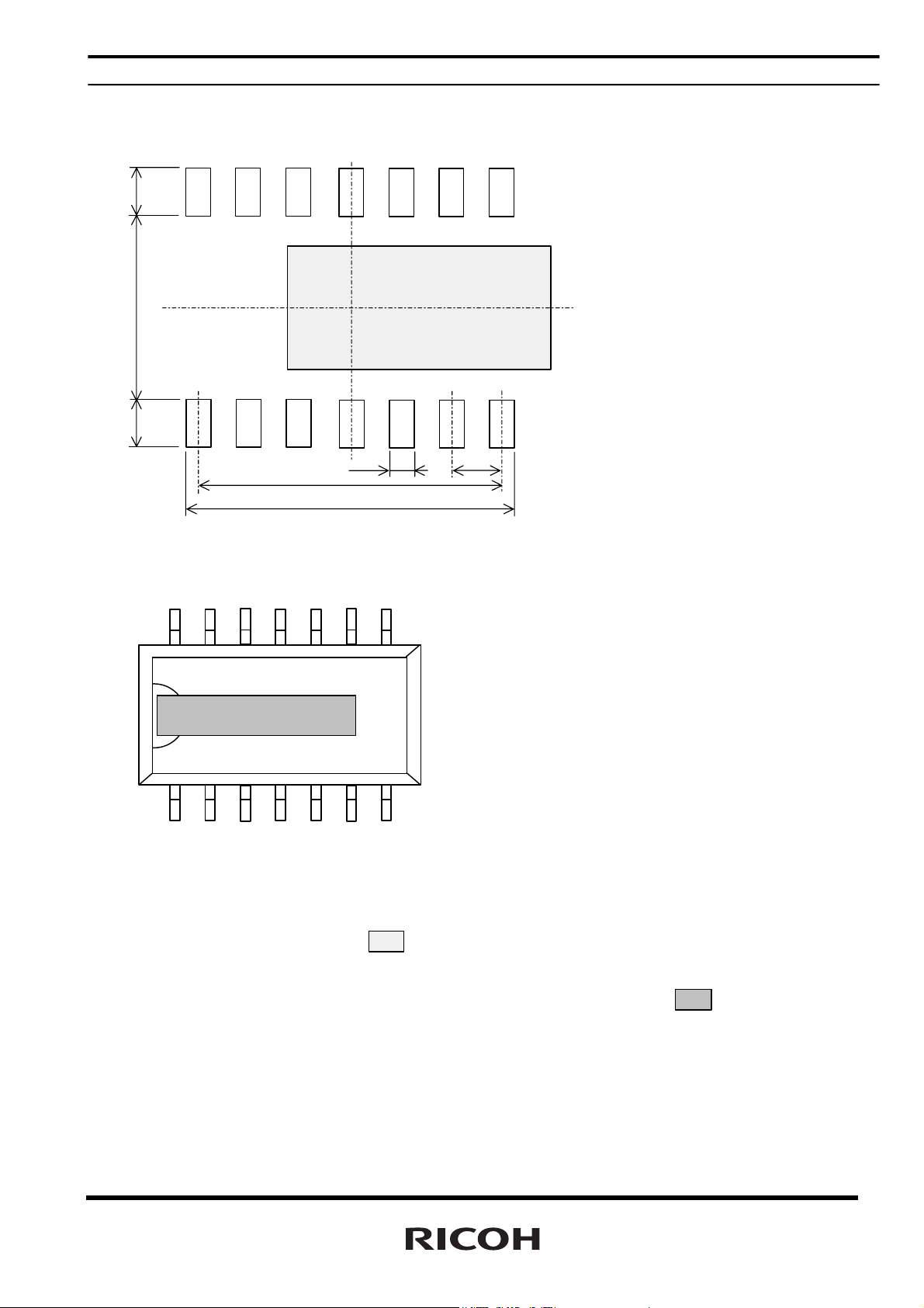
R2025S/D
y
Land Pattern (reference)
• R2025S (SOP14)
14
5.4 1.4 1.4
1
0.7
P 1.27x6=7.62
8.32
8
7
1.27
unit:mm
Package top view
14
8
46
1
7
1. Pad layout and size can modify by customers material, equipment, and method. Please adjust pad layout
according to your conditions.
2. In the mount area which desc ried as , is close t o the inside osc illator circ uit. To avoid the malfunction b
noise, check the other signal lines close to the area, do not intervene with the oscillator circuit.
3. A part of a metal case of the crystal may be seen in the area which described as in both sides of the
package. It has no influence on the characteristics and quality of the product.

• R2025D (SON22)
y
R2025S/D
22
4.0 0.7 0.7
0.8
1 11
0.7
P 0.5x10=5.0
0.25 0.75
14
0.25
0.5
1.4
0.8
0.75.25
unit : mm
Package top view Package bottom view
22 14
14
22
1 11
11
1
1. Pad layout and size can modify by customers material, equipment, and method. Please adjust pad layout
according to your conditions.
2. Any signal line should not pass through the area that described as in the land pattern. If a signal line is
located in that area, it may cause a short circuit with a tab suspens ion leads which is mark ed with in the
figure above or unnecessary remainder of cut lead.
3. In the mount area which descried as , is close to the inside osc illator circuit. To avoid the m alfunction b
noise, check the other signal lines close to the area, do not intervene with the oscillator circuit.
4. A part of a metal case of the crystal may be seen in the area that described as in both sides of the
package. It has no influence on the characteristics and quality of the product.
47

RICOHCOMPANY,LTD.
ElectronicDevicesCompany
●Shin-Yokohamaoffice(InternationalSales)
3-2-3,Shin-Yokohama,Kohoku-ku,YokohamaCity,Kanagawa222-8530,Japan
Phone:+81-45-477-1697Fax:+81-45-477-1698
RICOHEUROPE(NETHERLANDS)B.V.
●SemiconductorSupportCentre
Prof.W.H.Keesomlaan1,1183DLAmstelveen,TheNetherlands
P.O.Box114,1180ACAmstelveen
Phone:+31-20-5474-309Fax:+31-20-5474-791
RICOHELECTRONICDEVICESKOREACo.,Ltd.
11floor,Haesung1building,942,Daechidong,Gangnamgu,Seoul,Korea
Phone:+82-2-2135-5700Fax:+82-2-2135-5705
RICOHELECTRONICDEVICESSHANGHAICo.,Ltd.
Room403,No.2Building,690#BiBoRoad,PuDongNewdistrict,Shanghai201203,
People'sRepublicofChina
Phone:+86-21-5027-3200Fax:+86-21-5027-3299
RICOHCOMPANY,LTD.
ElectronicDevicesCompany
●Taipeioffice
Room109,10F-1,No.51,HengyangRd.,TaipeiCity,Taiwan(R.O.C.)
Phone:+886-2-2313-1621/1622Fax:+886-2-2313-1623
http://www.ricoh.com/LSI/
1.Theproductsandtheproductspecificationsdescribedinthisdocumentaresubjecttochangeor
discontinuationofproductionwithoutnoticeforreasons
suchasimprovement.Therefore,before
decidingtousetheproducts,pleaserefertoRicohsalesrepresentativesforthelatest
informationthereon.
2.Thematerialsinthisdocumentmaynotbecopiedorotherwisereproducedinwholeorinpart
withoutpriorwrittenconsentofRicoh.
3.Pleasebesuretotakeanynecessaryformalitiesunderrelevantlawsorregulationsbefore
exportingorotherwisetakingoutofyourcountrytheproductsorthetechnicalinformation
describedherein.
4.Thetechnicalinformationdescribedinthisdocumentshowstypicalcharacteristicsofand
exampleapplicationcircuitsfortheproducts.Thereleaseofsuchinformationisnottobe
construedasawarrantyoforagrantoflicenseunderRicoh'soranythirdparty'sintellectual
propertyrightsoranyotherrights.
5.
Theproductslistedinthisdocumentareintendedanddesignedforuseasgeneralelectronic
componentsinstandardapplications(officeequipment,telecommunicationequipment,
measuringinstruments,consumerelectronicproducts,amusementequipmentetc.).Those
customersintendingtouse
aproductinanapplicationrequiringextremequalityandreliability,
forexample,inahighlyspecificapplicationwherethefailureormisoperationoftheproduct
couldresultinhumaninjuryordeath(aircraft,spacevehicle,nuclearreactorcontrolsystem,
trafficcontrolsystem,automotiveand
transportationequipment,combustionequipment,safety
devices,lifesupportsystemetc.)shouldfirstcontactus.
6.Wearemakingourcontinuousefforttoimprovethequalityandreliabilityofourproducts,but
semiconductorproductsarelikelytofailwithcertainprobability.Inordertopreventanyinjuryto
personsordamagestopropertyresultingfromsuchfailure,customersshouldbecarefulenough
toincorporatesafetymeasuresintheirdesign,suchasredundancyfeature,firecontainment
featureandfail-safefeature.Wedonotassumeanyliability
orresponsibilityforanylossor
damagearisingfrommisuseorinappropriateuseoftheproducts.
7.Anti-radiationdesignisnotimplementedintheproductsdescribedinthisdocument.
8.
PleasecontactRicohsalesrepresentativesshouldyouhaveanyquestionsorcomments
concerningtheproductsorthetechnicalinformation.
RICOHCOMPANY.,LTD.ElectronicDevicesCompany
■
Ricoh presented with the Japan Management Quality Awa rd for 1999
.
Ricoh con tinually strives to promote cus tomer satisfacti on, and shares the achievements
of its ma nagement qualit y improvement pro gram with people and society.
■R ico h aw ard ed IS O 1 4001 certi ficat ion .
The Ricoh Group was awar ded IS O 14001 certifi cation, which is an internatio nal stan dard fo r
environm ental management sy stems, at b oth i ts do mestic and overseas productio n faci lities.
Our cur rent aim is to obtain ISO 14001 c ertification for all of our busines s office s.
Ricoh com pleted the orga nization of the Lead-free product ion for all of ou r products.
After Apr. 1, 200 6, we will ship out the lead free products only. Thus, all products that
will be shipped from now on comply with RoHS Directive.
 Loading...