

RICOH R2023K, R2023T Technical data

R2023K/T
2-wire Serial Interface Real Time Clock IC
NO.EA-124-070221
OUTLINE
The R2023K/T is a CMOS real-time clock IC connected to the CPU by two signal lines, SCL, SDA, and configured
to perform serial transmission of time and calendar data to the CPU. The periodic interrupt circuit is configured to
generate interrupt signals with six selectable interrupts ranging from 0.5 seconds to 1 month. The 2 alarm
interrupt circuits generate interrupt signals at preset times. As the oscillation circuit is driven under constant
voltage, fluctuation of the oscillator frequency due to supply voltage is small, and the time keeping current is small
(TYP. 0.45µA at 3V). The oscillation halt sensing circuit can be used to judge the validity of internal data in such
events as power-on; The supply voltage monitoring circuit is configured to record a drop in supply voltage below
two selectable supply voltage monitoring threshold settings. The 32.768kHz clock output function (CMOS output
with control pin) is intended to output sub-clock pulses for the external microcomputer. The oscillation adjustment
circuit is intended to adjust time counts with high precision by correcting deviations in the oscillation frequency of
the crystal oscillator. Since the package for these ICs are TSSOP10G (4.0x2.9x1.0: R2023T) or FFP12
(2.0x2.0x1.0: R2023K), high density mounting of ICs on boards is possible.
FEATURES
• Minimum Timekeeping supply voltage TYP:0.66 to 5.5v (Worst: 1.00V to 5.5v); VDD pin
• Low power consumption 0.45µA TYP at V
• Two signal lines (SCL, SDA) required for connection to the CPU.
• Time counters (counting hours, minutes, and seconds) and calendar counters (counting years, months, days,
and weeks) (in BCD format)
• Interrupt circuit configured to generate interrupt signals (with interrupts ranging from 0.5 seconds to 1 month) to
the CPU and provided with an interrupt flag and an interrupt halt
• 2 alarm interrupt circuits (Alarm_W for week, hour, and minute alarm settings and Alarm_D for hour and minute
alarm settings)
• With Power-on flag to prove that the power supply starts from 0V
• 32-kHz clock output pin (CMOS push-pull output with control pin)
• Supply voltage monitoring circuit with two supply voltage monitoring threshold settings
• Automatic identification of leap years up to the year 2099
• Selectable 12-hour and 24-hour mode settings
• High precision oscillation adjustment circuit
• Built-in oscillation stabilization capacitors (CG and CD)
• Package TSSOP10G (4.0mm x 2.9mm x 1.0mm: R2023T) FFP12 (2.0mm x 2.0mm x 1.0mm: R2023K)
• CMOS process
DD=3V (1.00µA MAX.)
1
R2023K/T
A
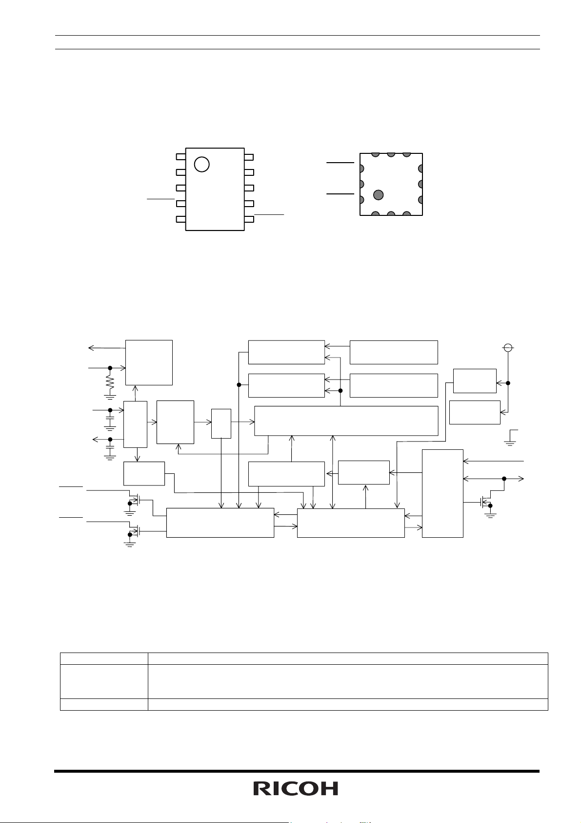
PIN CONFIGURATION
R2023T(TSSOP10G)
32KOUT
SCL
SDA
INTRB
BLOCK DIAGRAM
32KOUT
CLKC
OSCIN
OSCOUT
INTRA
32kHz
OUTPUT
CONTROL
OSC
OSC
DETECT
DIVIDER
CORREC
-TION
10
9
8
7
VDD
OSCIN
OSCOUT
CLKC
INTRAVSS
1
2
3
4
5 6
TOP VIEW
COMPARATOR_W
COMPARATOR_D
DIV
(SEC,MIN,HOUR,WEEK,DAY,MONTH,YEAR)
ADDRESS
DECODER
INTRA
INTRB
TIME COUNTER
R2023K(FFP12)
OSCOUT
CLKC
8
9
10
VSS
11
12
1
SD
TOP VIEW
ALARM_W REGISTER
(MIN,HOUR, WEEK)
ALARM_D REGISTER
(MIN,HOUR)
ADDRESS
REGISTER
OSCIN
7
2
SCL
VDD
6
(VSS)
5
(VSS)
4
3
32KOUT
CONTROL
VOLTAGE
DETECT
POWER_ON
I/O
VDD
RESET
VSS
SCL
SDA
INTRB
INTERRUPT CONTROL
SHIFT REGISTER
SELECTION GUIDE
Part Number is designated as follows:
R2023K-E2 ←Part Number
↑ ↑
R2023a-bb
Code Description
Designation of the package.
a
bb Designation of the taping type. Only E2 is available.
2
K: FFP12
T: TSSOP10G (Preliminary)

R2023K/T
PIN DESCRIPTION
Symbol Item Description
SCL Serial Clock
Line
SDA Serial Data Line The SDA pin is used to input and output data intended for writing and
INTRA
INTRB
32KOUT 32kHz Clock
CLKC Clock Control The CLKC pin is used to control output of the 32KOUT pin. The clock
OSCIN
OSCOUT
VDD
VSS
(VSS) Please connect to ground line, or do not connect any lines.
Interrupt
Output A
Interrupt
Output B
Output
Oscillation
Circuit
Input / Output
Positive/Negative
Power
Supply Input
The SCL pin is used to input clock pulses synchronizing the input and
output of data to and from the SDA pin. Allows a maximum input voltage of
5.5v regardless of supply voltage.
reading in synchronization with the SCL pin. Allows a maximum input
voltage of 5.5v regardless of supply voltage. Nch. open drain output.
INTRA
The
interrupt signals to the CPU. Disabled at power-on from 0V. N-channel
open drain output. Allows a maximum pull-up voltage of 5.5v regardless of
supply voltage.
INTRB
The
Disabled at power-on from 0V. N-channel open drain output. Allows a
maximum pull-up voltage of 5.5v regardless of supply voltage.
The 32KOUT pin is used to output 32.768-kHz clock pulses. The pin is
CMOS push-pull output. The output is disabled and held “L” when CLKC
pin is set to “L” or open, or certain register setting. This pin is enabled at
power-on from 0v.
output is disabled and held “L” when this pin is set to “L” or open.
Incorporated pull down register.
The OSCIN and OSCOUT pins are used to connect the 32.768-kHz crystal
oscillator (with all other oscillation circuit components built into the
R2023K/T).
The VDD pin is connected to the power supply. The VSS pin is grounded.
pin is used to output alarm interrupt (Alarm_D) and periodic
pin is used to output alarm interrupt (Alarm_W) to the CPU.
3
R2023K/T
ABSOLUTE MAXIMUM RATINGS
(VSS=0V)
Symbol Item Pin Name Description Unit
VDD Supply Voltage VDD -0.3 to +6.5 V
VI Input Voltage 1 SCL, SDA, CLKC -0.3 to +6.5 V
Output Voltage 1
Output Voltage 2 32KOUT -0.3 to V
PD Power Dissipation
Topt Operating Temperature -40 to +85
Tstg Storage Temperature -55 to +125
SDA,
Topt = 25°C
INTRA
INTRB
,
-0.3 to +6.5 VO
DD + 0.3
300 mW
V
°C
°C
RECOMMENDED OPERATING CONDITIONS
(VSS=0V, Topt=-40 to +85°C)
Symbol Item Pin Name Min, Typ. Max. Unit
Vaccess Supply Voltage Power supply voltage
for interfacing
with CPU
VCLK Time keeping Voltage
VCLKL Minimum Time keeping
Voltage
fXT Oscillation Frequency 32.768 kHz
VPUP Pull-up Voltage
*1) CGout is connected between OSCIN and VSS, CDout is connected between OSCOUT and VSS.
R2023K/T incorporates the capacitors between OSCIN and VSS, between OSCOUT and VSS.
Then normally, CGout and CDout are not necessary. For more detail, see “P.30 •Adjustment of oscillation
frequency”
*2) Crystal oscillator: CL=6-9pF, R1=50KΩ
CGout,CDout=0pF
*1), *2)
CGout,CDout=0pF
*1), *2)
INTRA
SCL, SDA
INTRB
,
,
1.7
*1)
1.00 5.50
0.66 1.00
5.5 V
5.5 V
V
4
R2023K/T
DC ELECTRICAL CHARACTERISTICS
(Unless otherwise specified:
V
SS=0V, VDD=3.0V, Topt=-40 to +85°C, Crystal oscillator 32768Hz,CL=7pF,R1=50kΩ)
Symbol Item Pin Name Conditions Min. Typ. Max. Unit
VIH “H” Input Voltage 0.8x
SCL, SDA,
CLKC
VIL “L” Input Voltage
IOH “H” Output
32KOUT VOH=VDD-0.5V -0.5 mA
DD=1.7 to 5.5V
V
VDD
-0.3 0.2x
Current
IOL1 32KOUT 0.5
IOL2
“L” Output
Current
INTRA
INTRB
IOL3
IIL Input Leakage
SDA
SCL VI=5.5V or VSS
Current
ICLKC Pull-down Resister
CLKC VI=5.5V 0.30 1.00
V
OL=0.4V
2.0
3.0
-1.0 1.0
VDD=5.5V
Input Leakage Current
IOZ
Output Off-state
Current
SDA,
INTRA
INTRB
,
IDD Time Keeping Current VDD VDD=3V,
O=5.5V or VSS
V
VDD=5.5V
SCL=SDA=CLKC=0V
-1 1
32KOUT=OFF
OUTPUT=OPEN
CGout=CDout=0pF
*1)
VDETH Supply Voltage
Monitoring Voltage
VDD
Topt=-30 to +70°C
1.45 1.60 1.75 V
“H”
VDETL Supply Voltage
Monitoring Voltage “L”
VDD
Topt=-30 to +70°C
1.15 1.30 1.45 V
*1) For time keeping current when outputting 32.768kHz from the 32KOUT pin, see “P.45 TYPICAL
CHARACTERISTICS”. For time keeping current when CGOUT, CDOUT is not equal to 0pF, see “P.30
•Adjustment of oscillation frequency”.
5.5
V
VDD
mA
µA
µA
µA
0.45 1.00
µA
5
R2023K/T
T
T
A
A
A
T
T
AC ELECTRICAL CHARACTERISTICS
Unless otherwise specified: VSS=0V,Topt=-40 to +85°C
Input and Output Conditions: V
Sym
-bol
f
SCL Clock Frequency 400 kHz
SCL
t
SCL Clock Low Time 1.3
LOW
t
SCL Clock High Time 0.6
HIGH
t
Start Condition Hold Time 0.6
HD;STA
t
Stop Condition Set Up Time 0.6
SU;STO
t
Start Condition Set Up Time 0.6
SU;STA
t
Data Set Up Time 200 ns
SU;DAT
t
Data Hold Time 0 ns
HD;DAT
t
SDA “L” Stable Time
PL;DAT
After Falling of SCL
t
SDA off Stable Time
PZ;DAT
After Falling of SCL
tR Rising Time of SCL and SDA
(input)
tF Falling Time of SCL and SDA
(input)
tSP Spike Width that can be
removed with Input Filter
t
Recovery Time from Stop
RCV
Condition to Start Condition
*) For reading/writing timing, see “P.28 Interfacing with the CPU •Data Transmission under Special Conditions”.
S
IH=0.8×VDD,VIL=0.2×VDD,VOH=0.8×VDD,VOL=0.2×VDD,CL=50pF
Item Condi-
Tions
Min. Typ. Max.
DD≥1.7V *1)
V
0.9
0.9
300 ns
300 ns
50 ns
62
Sr P
Unit
µs
µs
µs
µs
µs
µs
µs
µs
SCL
SDA(IN)
SDA(OUT)
S
Sr
t
LOW
t
PL;DA
t
SU;DA
t
HD;ST
Start Condition
Repeated Start Condition
Stop Condition
P
t
HIGH
t
HD;DA
t
PZ;DA
t
t
SU;ST
HD;ST
t
SP
t
SU;STO
6
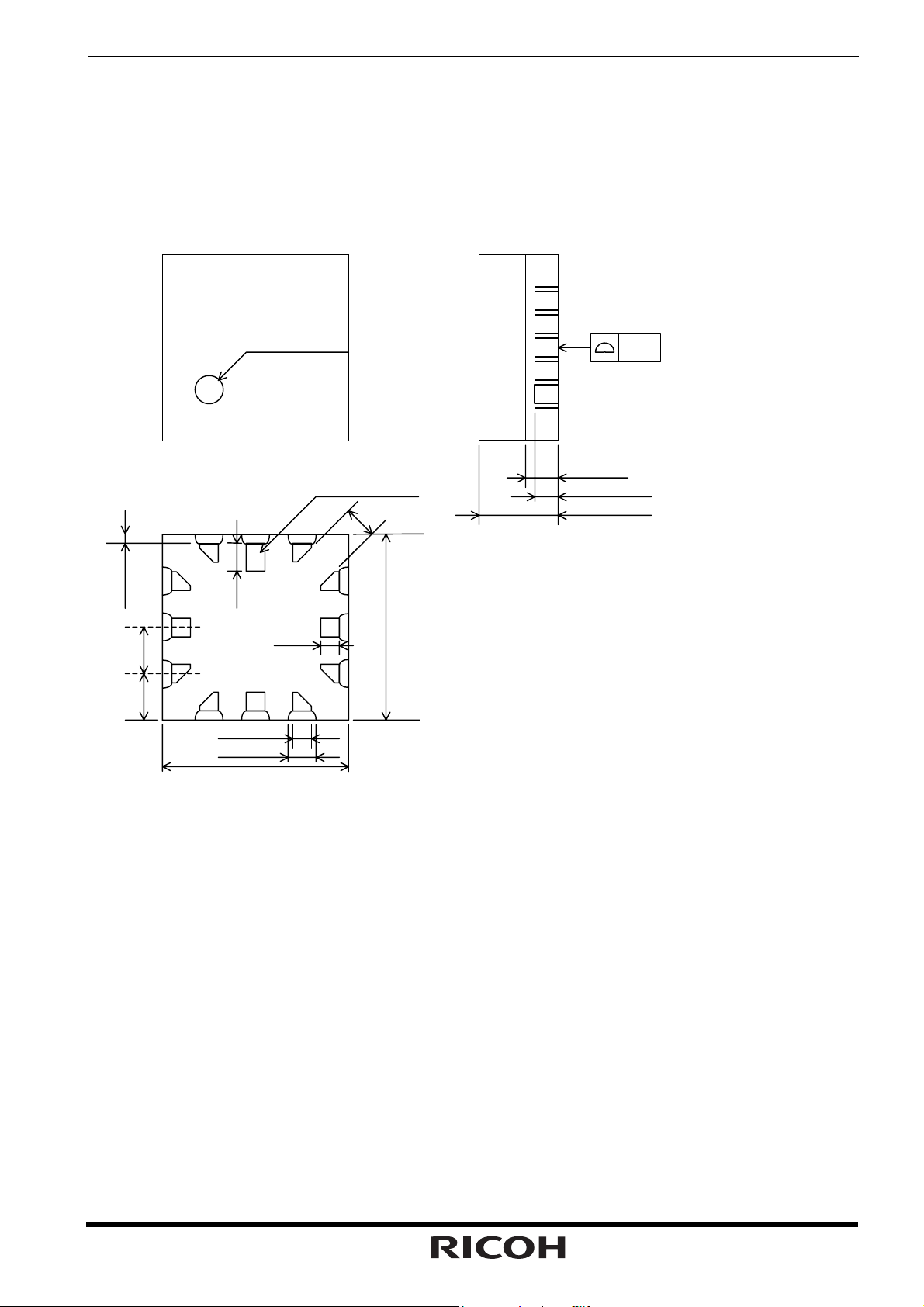
PACKAGE DIMENSIONS
• R2023K
9 7
R2023K/T
10
12
0.103
0.5
0.5
1PIN INDEX
2PIN INDEX
0.15
±
0.3
0.2±0.15
(BOTTOM VIEW)
6
0.05
4
3 1
0.35
0.1
±
2.0
0.35
0.25
1.0Max
0.17±0.1
0.27±0.15
2.0±0.1
unit: mm
7
R2023K/T
M
• R2023T
2.9±0.2
10
1
0.2±0.1
0.5
6
5
0.1
0.15
2.8±0.2
4.0±0.2
(0.75)
-0.05
+0.1
0.1
0 to 10
0.13
+0.1
-0.05
0.85±0.15
°
0.55±0.2
unit: mm
8

R2023K/T
GENERAL DESCRIPTION
• Interface with CPU
The R2023K/T is connected to the CPU by two signal lines, SCL and SDA, through which it reads and writes data
from and to the CPU. Since the I/O pin of SDA is open drain, data interfacing with a CPU different supply voltage
is possible by applying pull-up resistors on the circuit board. The maximum clock frequency of 400kHz (at
VDD≥1.7v) of SCL enables data transfer in I
• Clock and Calendar Function
The R2023K/T reads and writes time data from and to the CPU in units ranging from seconds to the last two digits
of the calendar year. The calendar year will automatically be identified as a leap year when its last two digits are a
multiple of 4. Consequently, leap years up to the year 2099 can automatically be identified as such.
*) The year 2000 is a leap year while the year 2100 is not a leap year.
• Alarm Function
The R2023K/T incorporates the alarm interrupt circuit configured to generate interrupt signals to the CPU at preset
times. The alarm interrupt circuit allows two types of alarm settings specified by the Alarm_W registers and the
Alarm_D registers. The Alarm_W registers allow week, hour, and minute alarm settings including combinations of
multiple day-of-week settings such as "Monday, Wednesday, and Friday" and "Saturday and Sunday". The
Alarm_D registers allow hour and minute alarm settings. The Alarm_W outputs from
Alarm_D outputs from
INTRA
pin. Each alarm function can be checked from the CPU by using a polling function.
• High-precision Oscillation Adjustment Function
2
C bus fast mode.
INTRB
pin, and the
The R2023K/T has built-in oscillation stabilization capacitors (CG and CD), which can be connected to an external
crystal oscillator to configure an oscillation circuit. Two kinds of accuracy for this function are alternatives. To
correct deviations in the oscillator frequency of the crystal, the oscillation adjustment circuit is configured to allow
correction of a time count gain or loss (up to ±1.5ppm or ±0.5ppm at 25°C) from the CPU. The maximum range is
approximately ±189ppm (or ±63ppm) in increments of approximately 3ppm (or 1ppm). Such oscillation frequency
adjustment in each system has the following advantages:
* Allows timekeeping with much higher precision than conventional RTCs while using a crystal oscillator with a
wide range of precision variations.
* Corrects seasonal frequency deviations through seasonal oscillation adjustment.
* Allows timekeeping with higher precision particularly with a temperature sensing function out of RTC, through
oscillation adjustment in tune with temperature fluctuations.
• Power-on Reset, Oscillation Halt Sensing Function and Supply Voltage Monitoring Function
The R2023K/T incorporates an oscillation halt sensing circuit equipped with internal registers configured to record
any past oscillation halt.
Power on reset function reset the control resisters when the system is powered on from 0V. At the same time, the
fact is memorized to the resister as a flag, thereby identifying whether they are powered on from 0V or battery
backed-up.
The R2023K/T also incorporates a supply voltage monitoring circuit equipped with internal registers configured to
record any drop in supply voltage below a certain threshold value. Supply voltage monitoring threshold settings can
be selected between 1.6V and 1.3V through internal register settings. The sampling rate is normally 1s.
The oscillation halt sensing circuit and the power-on reset flag are configured to confirm the established
invalidation of time data in contrast to the supply voltage monitoring circuit intended to confirm the potential
invalidation of time data. Further, the supply voltage monitoring circuit can be applied to battery supply voltage
monitoring.
9

R2023K/T
• Periodic Interrupt Function
The R2023K/T incorporates the periodic interrupt circuit configured to generate periodic interrupt signals aside
from interrupt signals generated by the alarm interrupt circuit for output from the
signals have five selectable frequency settings of 2 Hz (once per 0.5 seconds), 1 Hz (once per 1 second), 1/60 Hz
(once per 1 minute), 1/3600 Hz (once per 1 hour), and monthly (the first day of every month). Further, periodic
interrupt signals also have two selectable waveforms, a normal pulse form (with a frequency of 2 Hz or 1 Hz) and
special form adapted to interruption from the CPU in the level mode (with second, minute, hour, and month
interrupts). The condition of periodic interrupt signals can be monitored with using a polling function.
INTRA
pin. Periodic interrupt
• 32kHz Clock Output
The R2023K/T incorporates a 32-kHz clock circuit configured to generate clock pulses with the oscillation
frequency of a 32.768kHz crystal oscillator for output from the 32KOUT pin. The 32KOUT pin is CMOS push-pull
output and the output is enabled and disabled when the CLKC pin is held high, and low or open, respectively.
The 32-kHz clock output can be disabled by certain register settings but cannot be disabled without manipulation of
any two registers with different addresses to prevent disabling in such events as the runaway of the CPU. The
32-kHz clock circuit is enabled at power-on, when the CLKC pin is held high.
10
R2023K/T
A
A
A
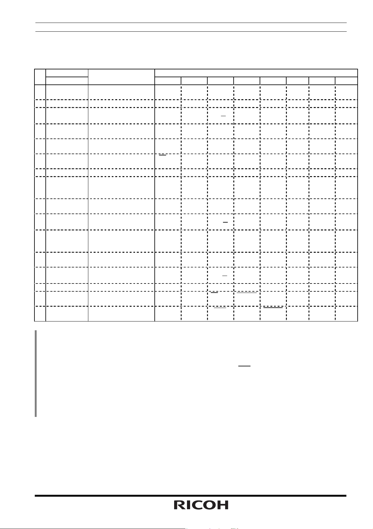
Address Mapping
Address Register Name D a t a
A3A2A1A0 D7 D6 D5 D4 D3 D2 D1 D0
0 0 0 0 0 Second Counter -
*2)
1 0 0 0 1 Minute Counter - M40 M20 M10 M8 M4 M2 M1
2 0 0 1 0 Hour Counter - - H20
3 0 0 1 1 Day-of-week
Counter
4 0 1 0 0 Day-of-month
Counter
5 0 1 0 1 Month Counter and
Century Bit
6 0 1 1 0 Year Counter Y80 Y40 Y20 Y10 Y8 Y4 Y2 Y1
7 0 1 1 1 Oscillation
Adjustment
Register *3)
8 1 0 0 0 Alarm_W
(Minute Register)
9 1 0 0 1 Alarm_W
(Hour Register)
A 1 0 1 0 Alarm_W
(Day-of-week
Register)
B 1 0 1 1 Alarm_D
(Minute Register)
C 1 1 0 0 Alarm_D
(Hour Register)
D 1 1 0 1 - - - - - - - -
E 1 1 1 0 Control Register 1
*3)
F 1 1 1 1 Control Register 2
*3)
Notes:
* 1) All the data listed above accept both reading and writing.
* 2) The data marked with "-" is invalid for writing and reset to 0 for reading.
* 3) When the PON bit is set to 1 in Control Register 2, all the bits are reset to 0 in Oscillation Adjustment
Register, Control Register 1 and Control Register 2 excluding the
* 4) When DEV=0, the oscillation adjustment circuit is configured to allow correction of a time count gain or loss
up
to ±1.5ppm. When DEV=1, the oscillation adjustment circuit is configured to allow correction of a time count
gain or loss up to or ±0.5ppm.
* 5) PON is a power-on-reset flag.
- - - - - W4 W2 W1
- - D20 D10 D8 D4 D2 D1
19
/20
DEV
*4)
- WM40 WM20 WM10 WM8 WM4 WM2 WM1
- - WH20
- WW6 WW5 WW4 WW3 WW2 WW1 WW0
- DM40 DM20 DM10 DM8 DM4 DM2 DM1
- - DH20
WALE DALE
VDSL VDET
S40 S20 S10 S8 S4 S2 S1
H10 H8 H4 H2 H1
P/
- - MO10 MO8 MO4 MO2 MO1
F6 F5 F4 F3 F2 F1 F0
WH10 WH8 WH4 WH2 WH1
WP/
DH10 DH8 DH4 DH2 DH1
DP/
12
XST
/24
CLEN2
PON
*5)
XST
TEST CT2 CT1 CT0
CLEN1
bit.
CTFG WAFG DAFG
11
R2023K/T
Register Settings
• Control Register 1 (ADDRESS Eh)
D7 D6 D5 D4 D3 D2 D1 D0
WALE DALE
WALE DALE
0 0 0 0 0 0 0 0 Default Settings *)
*) Default settings: Default value means read / written values when the PON bit is set to “1” due to VDD
power-on from 0 volts.
12
12
/24
/24
CLEN2
CLEN2
(1) WALE, DALE Alarm_W Enable Bit, Alarm_D Enable Bit
WALE,DALE Description
0 Disabling the alarm interrupt circuit (under the control of the settings
of the Alarm_W registers and the Alarm_D registers).
1 Enabling the alarm interrupt circuit (under the control of the settings
of the Alarm_W registers and the Alarm_D registers)
12
(2)
(3)
/24
12
/24
0 Selecting the 12-hour mode with a.m. and p.m. indications. (Default)
1 Selecting the 24-hour mode
Setting the
Setting the
CLEN2
Setting the
specifies generating clock pulses with the oscillation frequency of the 32.768-kHz crystal oscillator for output
from the 32KOUT pin. Conversely, setting both the
specifies disabling (”L”) such output.
12
/24 bit to 0 and 1 specifies the 12-hour mode and the 24-hour mode, respectively.
24-hour mode 12-hour mode 24-hour mode 12-hour mode
00 12 (AM12) 12 32 (PM12)
01 01 (AM 1) 13 21 (PM 1)
02 02 (AM 2) 14 22 (PM 2)
03 03 (AM 3) 15 23 (PM 3)
04 04 (AM 4) 16 24 (PM 4)
05 05 (AM 5) 17 25 (PM 5)
06 06 (AM 6) 18 26 (PM 6)
07 07 (AM 7) 19 27 (PM 7)
08 08 (AM 8) 20 28 (PM 8)
09 09 (AM 9) 21 29 (PM 9)
10 10 (AM10) 22 30 (PM10)
11 11 (AM11) 23 31 (PM11)
12
/24 bit should precede writing time data
32kHz Clock Output Bit 2
CLEN2
CLEN2
0 Enabling the 32-kHz clock circuit (Default)
1 Disabling the 32-kHz clock circuit
12
/24-hour Mode Selection Bit
Description
bit or the
CLEN1
bit (D3 in the control register 2) to 0, and the CLKC pin to high
(4) TEST Test Bit
TEST Description
0 Normal operation mode. (Default)
1 Test mode.
The TEST bit is used only for testing in the factory and should normally be set to 0.
TEST CT2 CT1 CT0 (For Writing)
TEST CT2 CT1 CT0 (For Reading)
(Default)
Description
CLEN1
and
CLEN2
bit to 1 or CLKC pin to low
12
R2023K/T
A
(5) CT2, CT1, and CT0 Periodic Interrupt Selection Bits
Description CT2 CT1 CT0
Wave form
mode
0 0 0 - OFF(H) (Default)
0 0 1 - Fixed at “L”
0 1 0 Pulse Mode
*1)
0 1 1 Pulse Mode
*1)
1 0 0 Level Mode
*2)
1 0 1 Level Mode
*2)
1 1 0 Level Mode
*2)
1 1 1 Level Mode
*2)
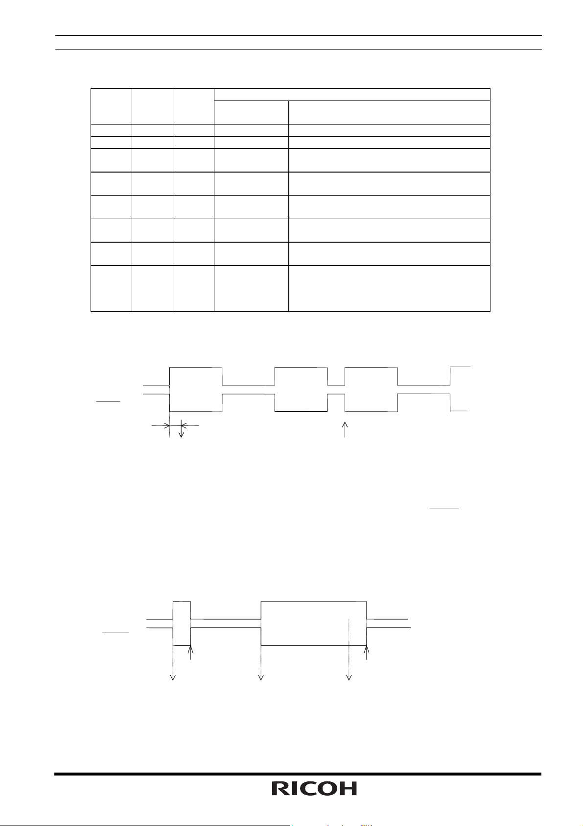
* 1) Pulse Mode: 2-Hz and 1-Hz clock pulses are output in synchronization with the increment of the second
counter as illustrated in the timing chart below.
Interrupt Cycle and Falling Timing
2Hz (Duty50%)
1Hz (Duty50%)
Once per 1 second (Synchronized with
second counter increment)
Once per 1 minute (at 00 seconds of
every minute)
Once per hour (at 00 minutes and 00
seconds of every hour)
Once per month (at 00 hours, 00
minutes,
and 00 seconds of first day of every
month)
CTFG Bit
INTRA Pin
pprox. 92µs
(Increment of second counter)
Rewriting of the second counter
In the pulse mode, the increment of the second counter is delayed by approximately 92 µs from the falling
edge of clock pulses. Consequently, time readings immediately after the falling edge of clock pulses may
appear to lag behind the time counts of the real-time clocks by approximately 1 second. Rewriting the
second counter will reset the other time counters of less than 1 second, driving the
INTRA
pin low.
* 2) Level Mode: Periodic interrupt signals are output with selectable inte rrupt cycle settings of 1 second, 1
minute, 1 hour, and 1 month. The increment of the second counter is synchronized with the falling edge of
periodic interrupt signals. For example, periodic interrupt signals with an interrupt cycle setting of 1 second
are output in synchronization with the increment of the second counter as illustrated in the timing chart below.
CTFG Bit
INTRA Pin
Setting CTFG bit to 0
(Increment of
second counter)
(Increment of
second counter)
Setting CTFG bit to 0
(Increment of
second counter)
13
R2023K/T
*1), *2) When the oscillation adjustment circuit is used, the interrupt cycle will fluctuate once per 20sec. or
60sec. as follows:
Pulse Mode: The “L” period of output pulses will increment or decrement by a maximum of ±3.784 ms. For
example, 1-Hz clock pulses will have a duty cycle of 50 ±0.3784%.
Level Mode: A periodic interrupt cycle of 1 second will increment or decrement by a maximum of ±3.784 ms.
• Control Register 2 (Address Fh)
D7 D6 D5 D4 D3 D2 D1 D0
VDSL VDET
VDSL VDET
0 0
*) Default settings: Default value means read / written values when the PON bit is set to “1” due to VDD
power-on from 0 volts.
XST
XST
Indefinite
(1) VDSL VDD Supply Voltage Monitoring Threshold Selection Bit
VDSL Description
0 Selecting the VDD supply voltage monitoring threshold setting of
1.6v.
1 Selecting the VDD supply voltage monitoring threshold setting of
1.3v.
The VDSL bit is intended to select the VDD supply voltage monitoring threshold settings.
(2) VDET Supply Voltage Monitoring Result Indication Bit
VDET Description
0 Indicating supply voltage above the supply voltage monitoring
threshold settings.
1 Indicating supply voltage below the supply voltage monitoring
threshold settings.
Once the VDET bit is set to 1, the supply voltage monitoring circuit will be disabled while the VDET bit will
hold
the setting of 1. The VDET bit accepts only the writing of 0, which restarts the supply voltage monitoring
circuit. Conversely, setting the VDET bit to 1 causes no event.
XST
(3)
The
halt
sensing. The
Oscillation Halt Sensing Monitor Bit
XST
0 Sensing a halt of oscillation
1 Sensing a normal condition of oscillation
XST
accepts the reading and writing of 0 and 1. The
XST
bit will hold 0 even after the restart of oscillation.
(4) PON Power-on-reset Flag Bit
PON Description
0 Normal condition
1 Detecting VDD power-on -reset (Default)
The PON bit is for sensing power-on reset condition.
* The PON bit will be set to 1 when VDD power-on from 0 volts. The PON bit will hold the setting of 1 even
after power-on.
* When the PON bit is set to 1, all bits will be reset to 0, in the Oscillation Adjustment Register, Control
Register 1, and Control Register 2, except
* The PON bit accepts only the writing of 0. Conversely, setting the PON bit to 1 causes no event.
14
PON
PON
1 0 0 0 0 Default Settings *)
CLEN1
CLEN1
XST
and PON. As a result,
CTFG WAFG DAFG (For Writing)
CTFG WAFG DAFG (For Reading)
(Default)
(Default)
Description
XST
bit will be set to 0 when the oscillation
INTR
pin stops outputting.
R2023K/T
A
A
CLEN1
(5)
(6) CTFG Periodic Interrupt Flag Bit
The CTFG bit is set to 1 when the periodic interrupt signals are output from the
CTFG bit accepts only the writing of 0 in the level mode, which disables (“H”) the
enabled (“L”) again in the next interrupt cycle. Conversely, setting the CTFG bit to 1 causes no event.
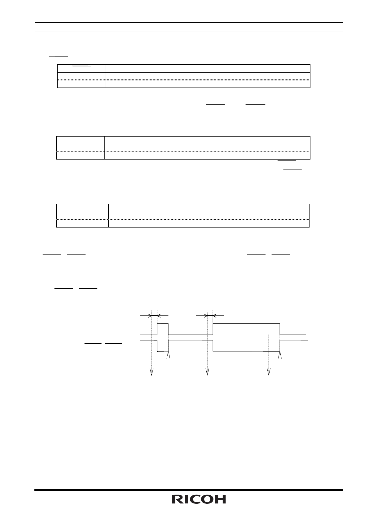
(7) WAFG,DAFG Alarm_W Flag Bit and Alarm_D Flag Bit
The WAFG and DAFG bits are valid only when the WALE and DALE have the setting of 1, which is caused
approximately 61µs after any match between current time and preset alarm time specified by the Alarm_W
registers and the Alarm_D registers. The WAFG (DAFG) bit accepts only the writing of 0.
INTRA
again at the next preset alarm time. Conversely, setting the WAFG and DAFG bits to 1 causes no event.
The WAFG and DAFG bits will have the reading of 0 when the alarm interrupt circuit is disabled with the
WALE and DALE bits set to 0. The settings of the WAFG and DAFG bits are synchronized with the output of
the
32kHz Clock Output Bit 1
CLEN1
0 Enabling the 32-kHz clock circuit (Default)
1 Disabling the 32-kHz clock circuit
Setting the
CLEN1
bit or the
CLEN2
bit (D4 in the control register 1) to 0, and the CLKC pin to high
specifies generating clock pulses with the oscillation frequency of the 32.768-kHz crystal oscillator for output
from the 32KOUT pin. Conversely, setting both the
specifies disabling (”L”) such output.
CTFG Description
0 Periodic interrupt output = “H” (Default)
1 Periodic interrupt output = “L”
WAFG,DAFG Description
0 Indicating a mismatch between current time and preset alarm time (Default)
1 Indicating a match between current time and preset alarm time
INTRB
(
INTRA
) pin outputs off (“H”) when this bit is set to 0. And
INTRB
(
) pin as shown in the timing chart below.
pprox. 61µs
Description
CLEN1
pprox. 61µs
and
CLEN2
bit to 1 or CLKC pin to low
INTRA
INTRA
INTRA (INTRB
pin (“L”). The
pin until it is
) pin outputs “L”
WAFG(DAFG) Bit
INTRB (INTRA) Pin
(Match between
current time and
preset alarm time)
Writing of 0 to
WAFG(DAFG) bit
(Match between
current time and
preset alarm time)
(Match between
current time and
preset alarm time)
Writing of 0 to
WAFG(DAFG) bit
15
 Loading...