How it Works
Log In / Sign Up
Buy Points
How it Works
FAQ
Contact Us
Questions and Suggestions
Users
RICOH
Loading...
R
R1162N371B
R1162N371D
R1162N381B
R1162N381D
R1162N391B
R1162N391D
R1162N401B
R1162N401D
R1162x
R1163x
2
R1170X
3
R1171x
2
R1172x
2
R1173x
2
R1180x
2
R1182x
2
R1183Z
R1190x
2
R1191x
R1200x
2
R1201N
R1201x
R1202x
R1203x
2
R1204x
2
R1205x
2
R1210N
R1210Nxx1x
R1210Nxx2x
R1211x
2
R1212D
2
R1213K
2
R1215D
2
R1218x
2
R1224N
2
R1225N
2
R1232D
2
R1242S
2
R1243x
2
R1245x
2
R1250V××1A
R1280D002A-TR
R1280D002B-TR
R1280D002C-TR
R1283K
R1283x
R1286K
2
R1290x
R1500x
2
R1501x
2
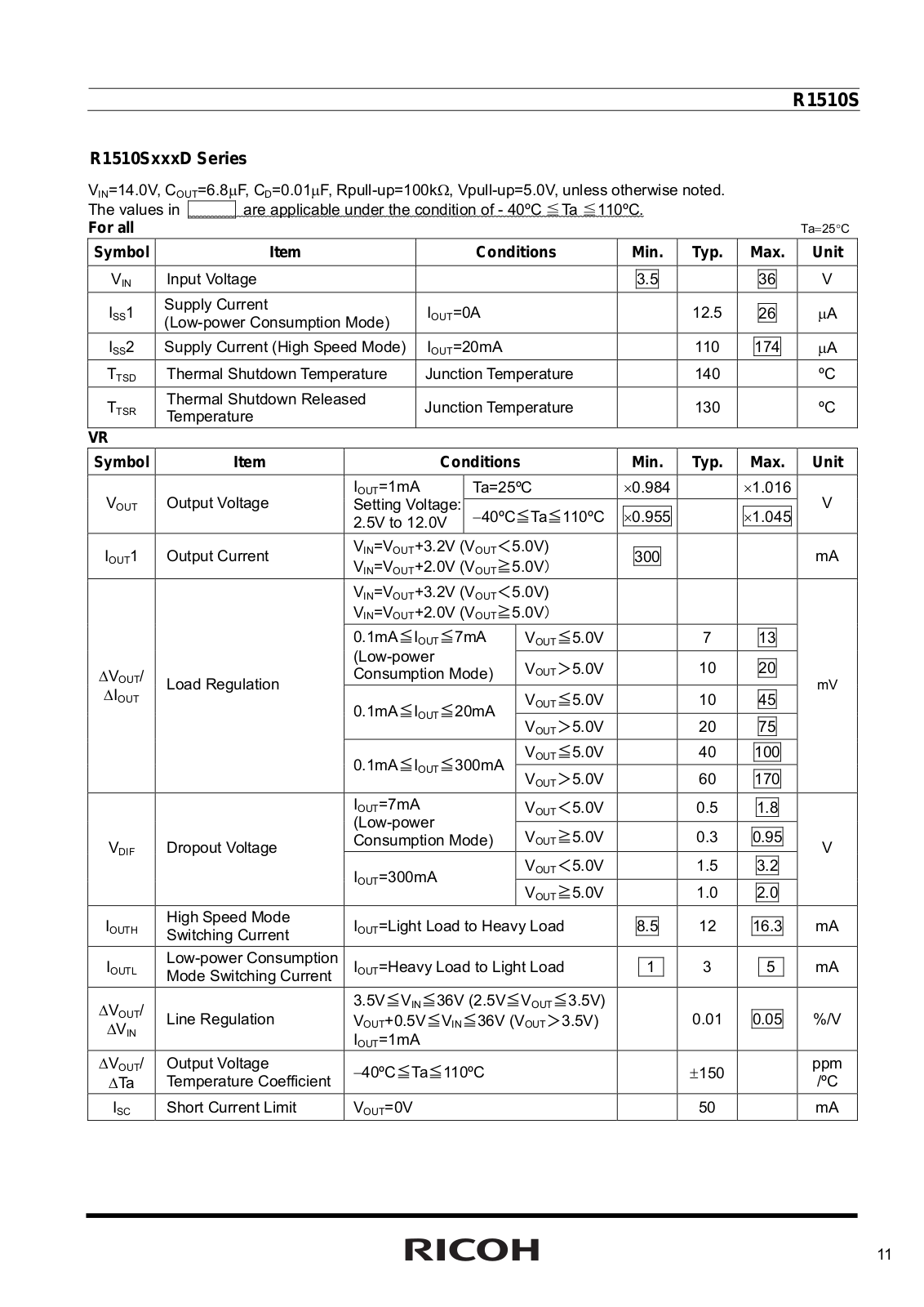
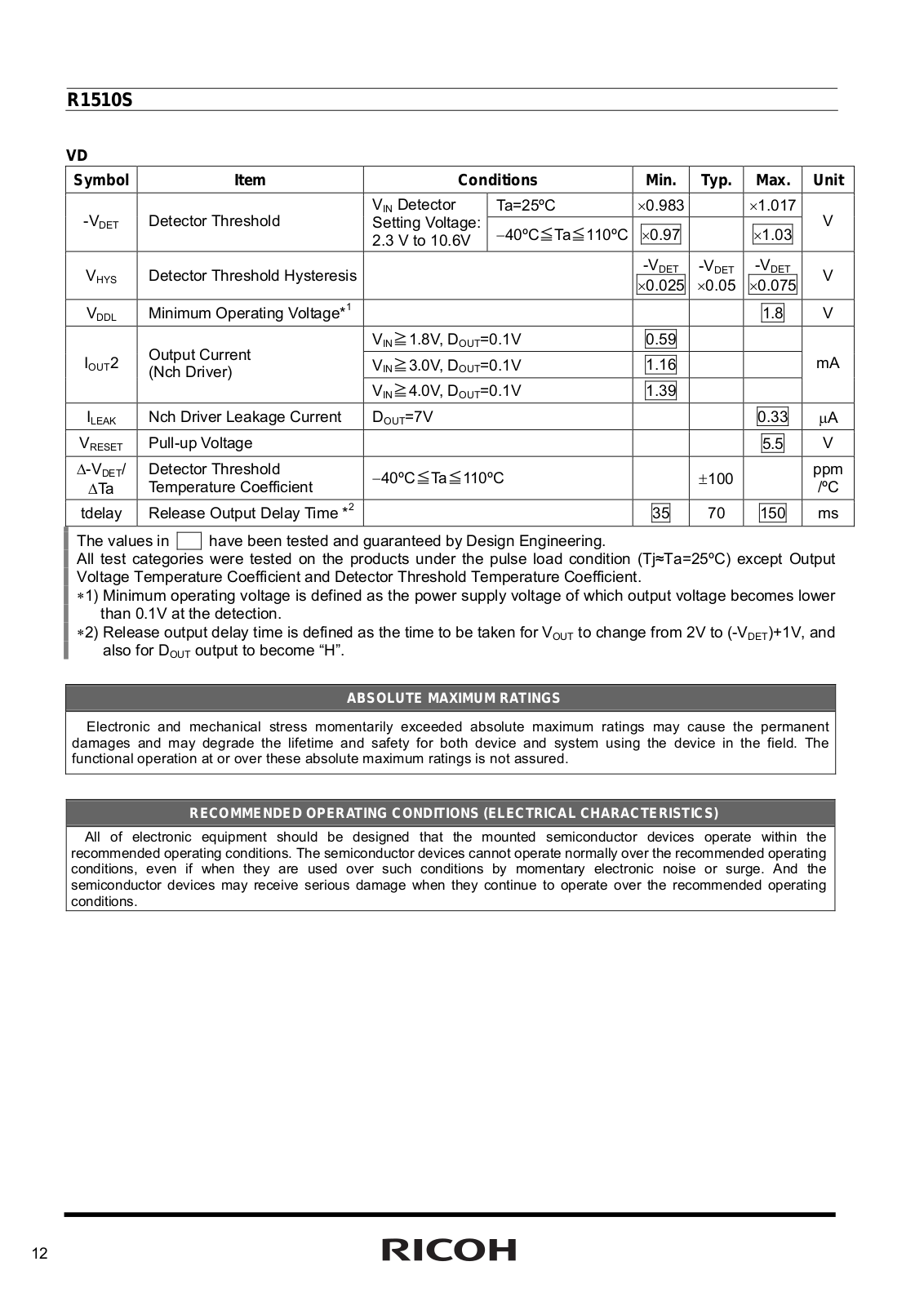
R1510S
2
R1514x
2
R1515x
2
R1516x
R1v
9
R2
8
R2023K
R2023T
R2025D
R2025S
R2033K
R2033T
R2043K
R2043T
R2045D
R2045S
R2051
R2061
R2062
R2221L
R2221T
R2223L
R2223T
R3
8
R30
7
R3111 Series
R3111x
R3111x Series
2
R3111xxx1A-C
R3112x
R3114x
R3116x
R3117xxx1
R3117xxx2
R3117xxx3
R3117xxx4
R3118x
R3119N
2
R3132x
2
R3133D
R3133x
R3134x
R3150N
R3200x
2
R4
7
R40
6
R5
6
R50
10
R5101G001A
R5101G002A
Loading...
Loading...
Nothing found
R1510S
Technical data
40 pgs
720.21 Kb
0
Technical data
2 pgs
237.41 Kb
0
Table of contents
Loading...
RICOH R1510S Technical data
...
RICOH Technical data
Download
Specifications and Main Features
Frequently Asked Questions
User Manual
Download
Loading...
+
28
hidden pages
Unhide
You need points to download manuals.
1 point = 1 manual.
You can buy points or you can get point for every manual you upload.
Buy points
Upload your manuals
 Loading...