R1500x Series
500mA 24V Input VR
The R1500x Series are CMOS-based voltage regulators featuring 500mA output current and 24V input voltage. R1500x provides high
input voltage operation and low on-resistance (at V
protection circuit built into conventional regul ators, R1500x con tains a thermal shutdown circuit. Besides the low suppl y current by
CMOS, the operating temperature is -40°C to 105°C and the m aximum input voltage is 24V, the R1515x series are very suitable for
power source of car accessories.
FEATURES
• Supply Current (ISS) ························Typ. 70μA (VIN=SET VOUT+1.0V)
• Standby Current (Istandby) ·················Typ. 0.1μA (VIN=24.0V, CE="L")
• Dropout Voltage (VDIF)·····················Typ. 0.115V (IOUT=200mA, VOUT=5.0V)
• Input Voltage Range (VIN) ···············
4.0V to 24.0V (Absolute maximum rating: 36.0V)
• Ripple Rejection (RR)····················· Typ. 60dB (f=1kHz, VOUT
Typ. 50dB (f=1kHz, V
• Output Voltage Range (VOUT)·········· 3.0V to 12.0V (internally fixed)
• Output Voltage Accuracy ················± 2%
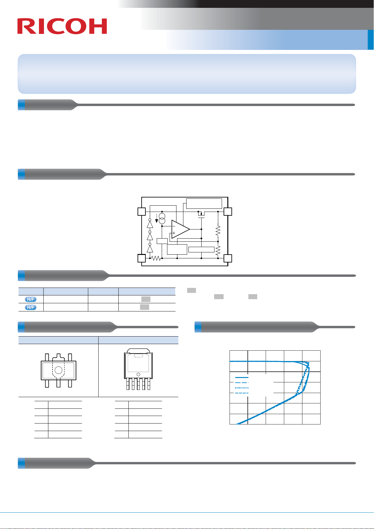
BLOCK DIAGRAM
VDD V
OUT=10V, below 0.6Ω) because of using CMOS transistor. In addition to a fold-back
• Temp. coeff of Output Voltage ···················Typ. ±100ppm/°C
• Line Regulation········································ Typ. 0.05%/V
• Fold-back Protection Circuit····················· Current limit Typ. 65mA
• Thermal Shutdown Circuit························Stops at Typ. 160°C.
≤
6.0V)
OUT > 6.0V)
• Package······················································ SOT-89-5,TO-252-5-P2
• Ceramic capacitors can be used.·············CIN=0.47μF or more
C
OUT=10μF or more
R1500xxxxB
Thermal Shutdown
Circuit
OUT
Vref
Short
Protection
Current Limit
CE GND
SELECTION GUIDES
Halogen Free
Package
Q'ty per Reel
SOT-89-5 1,000 pcs
TO-252-5-P2 3,000 pcs
Part No.
R1500H.xxx B-T1-FE
R1500J.xxx B-T1-FE
.xxx : Specify the output voltage within the range of
3.0V (.030.) to 12.0V (.120.) in 0.1V steps
PACKAGES (Top View) TYPICAL CHARACTERISTIC
SOT-89-5 TO-252-5-P2
5 4
1 3
2
1 VDD
GND
GND
∗
∗
2
3
4 CE
5 VOUT
) The GND pin must be wired together when it is mounted on board
∗
1 2 3 4 5
1 VDD
2
GND
3
GND
4 CE
5 VOUT
∗
∗
R1500x120B Output Voltage vs. Output Current
14
12
(V)
10
OUT
8
6
4
Output Voltage V
2
0
0 600200 800400 1000
VIN=12.5V
VIN=13.0V
IN=15.0V
V
VIN=16.0V
Output Current I
APPLICATIONS
• Power source for home appliances such as refrigerators, rice cookers, electric water warmers, etc
• Power source for car audio equipment, car navigation systems, ETC systems, etc
• Power source for laptop personal computers, digital TVs, cordless phones, and private LAN systems for home, etc
• Power source for office equipment machines such as copiers, printers, facsimiles, scanners, etc
OUT (mA)
No.EK-151-101001 CMOS Voltage Regulator

R1500x Series CMOS Voltage Regulator
RP171x
RP170x
R1191x
RP132x
RP173x
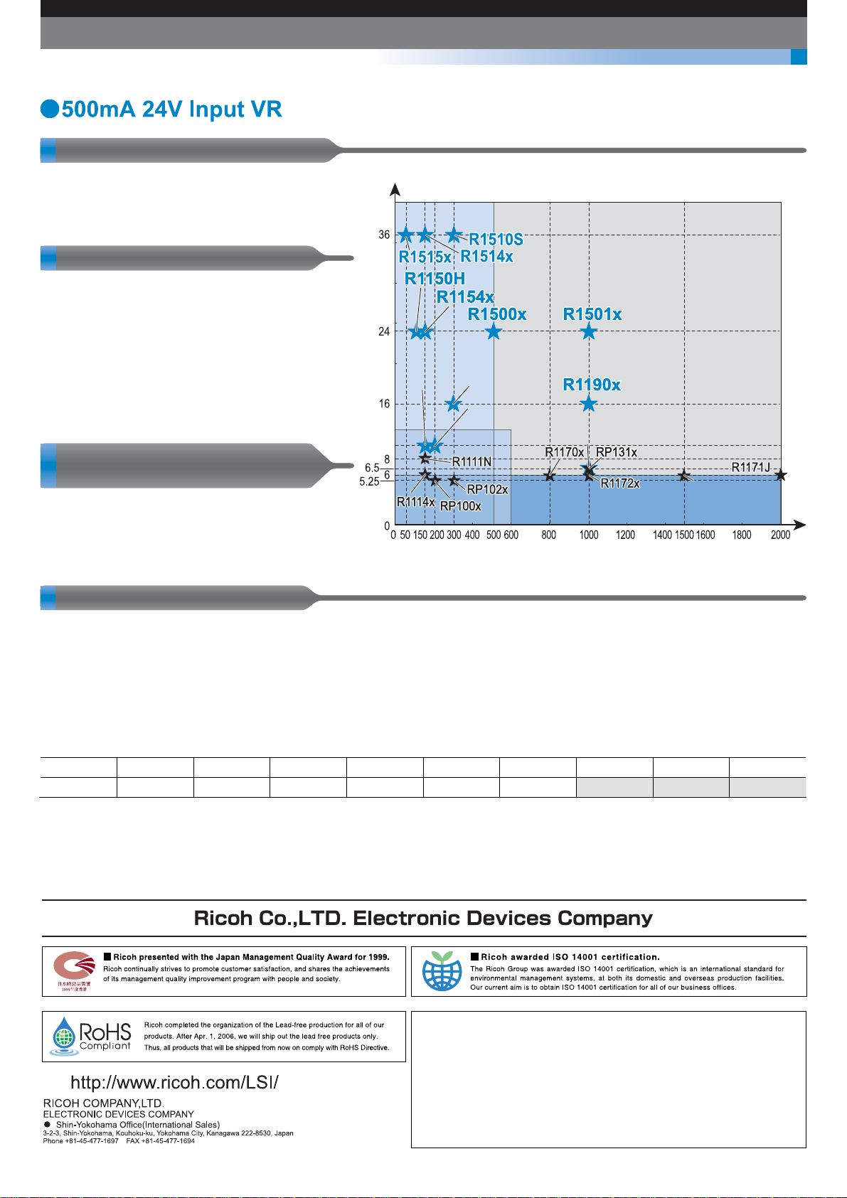
CMOS type high input voltage area
CMOS type large current range
CMOS area
R1171S
500mA 24V Input VR
MAXIMUM INPUT VOLTAGE 24V
The CMOS type regulator has been introduced into the
high input voltage area where only bipolar type could
previously operate.
CMOS type high input voltage areaCMOS type high input voltage area
ADOPTION OF DMOS PROCESS
The DMOS (Double Diffused MOS) transistor adopted by
R1500x is characterized by a double diffusion structure
which comprises a low density n-type (channel) diffused
layer and a high density p-type (sources) diffused layer
from the edge of the gate electrode. The R1500x series
possess outstanding properties of high operating voltage
and low on-resistance, which have been achieved by the
channel length scaled down to submicron dimensions and
decreased thickness of the gate oxide film.
RP171xRP171x
Maximum input voltage (V)
10
R1191xR1191x
RP170xRP170x
RP173xRP173x
CMOS area CMOS area
RP132xRP132x
MAXIMUM OPERATING AMBIENT
TEMPERATURE 105°C
Unlike Ricoh’s conventional regulators, the operating
ambient temperature range of the R1500x Series is rated
from -40°C to 105°C that makes it suitable for use in
automotive and industrial applications involving higher
temperatures.
CMOS type large current rangeCMOS type large current range
Output current (mA)
R1171SR1171S
Thermal Shutdown Circuit
The Thermal Shutdown Circuit shown in the block diagram detects an increase in temperature, stops operation, and protects the regulator from
being damaged by a short circuit in the output pin (V
The Thermal Shutdown Circuit stops operation of the regulator when the junction temperature of the regulator exceeds 160°C. Moreover, when the junction
temperature decreases to a level below 135°C after the regulator has stopped, the regulator resumes to normal operation.
As a result, the operation of the Thermal Shutdown Circuit causes the regulator repeatedly to turn OFF and ON till the causes of overheating are
removed. As a consequence, a pulse shaped output voltage occurs. Care should be taken to prevent this situation.
In the datasheet it is shown as a thermal shutdown detection temperature (T
Products with a built-in Thermal Shutdown Circuit
R1150H R1154x R1170x R1171x R1172x R1173x R1190x R1191x R1500x R1501x
R1510S R1514x R1515x RP111x RP131x RP170x RP171x
OUT) and ground pin (GND).
TSD) and a thermal shutdown release temperature (TTSR).
The currently available information as of October 2010 is provided in this New Product News.
EK-151-101001
 Loading...