

RICOH R1280D002A-TR, R1280D002B-TR, R1280D002C-TR Datasheet

2001.6.16
2CH PWM DC/DC Controller
R1280D002X Series
OUTLINE
■■■■
The R1280D002X Series are 2-channel PWM Step-up (as Channel 1)/Inverting (as Channel 2) DC/DC converter
controllers with CMOS process.
Each of the R1280D002X Series consists of an oscillator, a PWM control circuit, a reference voltage unit, an error
amplifier, a reference current unit, a protection circuit, and an under voltage lockout (UVLO) circuit. A high efficiency
Step-up/Inverting DC/DC converter can be composed of this IC with inductors, diodes, power MOSFETs, resisters,
and capacitors. Each Output Voltage can be adjustable with external resistors, while soft-start time can be adjustable
with external capacitors..
Maximum Duty Cycle of R1280D002A and C series can be also adjustable with external resistors.
Maximum Duty Cycle of R1280D002B is built-in as 90%(TYP.).
When CE pin of R1280D002B is set at GND level, this IC turns off external power MOSFETs of Step-up/Inverting as
Standby-mode.
Standby current is typically 0µA.
As for a protection circuit, if Maximum duty cycle of either Step-up DC/DC converter side or Inverting DC/DC
converter side is continued for a certain time, the R1280D Series latch both external drivers with their off state by its
Latch-type protection circuit. Delay time for protection is internally fixed typically at 100ms. To release the protection
circuit, restart with power-on (Voltage supplier is equal or less than UVLO detector threshold level), or as for
R1280D002B, once after making the circuit be stand-by with chip enable pin and enable the circuit again.
FEATURES
■■■■
●
Input Voltage Range • • • • • • • • • • • • • 2.5V to 5.5V
● Built-in Latch-type Protection Function by monitoring duty cycle (Fixed Delay Time TYP. 100ms)
● Oscillator Frequency • • • • • • • • • • • • • 700kHz(R1280D002A,B)/200kHz(r1280D002C)
● Maximum Duty Cycle • • • • • • • • • • • • • TYP. 90%(Only applied to R1280D002B Series)
● High Reference Voltage Accuracy • • • • • • ±1.5%
● U.V.L.O. Threshold • • • • • • • • • • • TYP. 2.2V (Hysteresis: TYP. 0.1V)
● Small Package • • • • • • • • • • • • • • • • thin SON-10 (package thickness MAX. 0.9mm)
APPLICATIONS
■■■■
● Constant Voltage Power Source for portable equipment.
● Constant Voltage Power Source for LCD and CCD.
Rev. 1.10 - 1 -

BLOCK DIAGRAM
A
■■■■
●
R1280D002A/C
V
FB1
DTC1
MPOUT1
Vrefout
●
R1280D002B
OSC
CH
1
Vref1
Vrefout
V
FB2
DTC2
CH
UVLO
Latch
Delay Circuit
2
EXT1
V
IN
GND
EXT2
DTC1
V
FB1
CE
Vrefout
V
FB2
CHIP ENABLE
Vrefout
OSC
CH1
Vref1
DTC2
CH
UVLO
2
Latch
Delay Circuit
EXT1
V
IN
GND
EXT2
Rev.1.10 - 2 -
SELECTION GUIDE
(
)
■
The mask option for the ICs can be selected at the user's request. The selection can be made with designating the
part number as shown below;
R1280D002X-TR
↑
a b
Code Contents
Designation of Mask Option :
a
A version: fosc=700kHz, with External Phase Compensation for Channel 1.
B version: fosc=700kHz, with Internal Phase Compensation and standby mode.
C version: fosc=200kHz, with External Phase Compensation for Channel 1
↑
←
Part Number
b
PIN CONFIGURATION
■■■■
●
SON10
10 6
mark side
1 5
PIN DESCRIPTION
■■■■
Designation of Taping Type :
(Refer to Taping Specifications.)
●
R1280D002A/C
Pin No. Symbol Description
1 EXT1 External Transistor of Channel 1 Drive Pin (CMOS Output)
2 GND Ground Pin
3 AMPOUT1 Amplifier Output Pin of Channel 1
4 DTC1 Maximum Duty Cycle of Channel 1 Setting Pin
5V
6V
7 DTC2 Maximum Duty Cycle of Channel 2 Setting Pin
8 Vrefout Reference Output Pin
9V
10 EXT2 External Transistor of Channel 2 Drive Pin (CMOS Output)
Rev. 1.10 - 3 -
FB1
FB2
IN
Feedback pin of Channel 1
Feedback pin of Channel 2
Voltage Supply Pin of the IC

●
R1280D002B
Pin No. Symbol Description
1 EXT1 External Transistor of Channel 1 Drive Pin (CMOS Output)
2 GND Ground Pin
3 CE Chip Enable Pin
4 DTC1 Maximum Duty Cycle of Channel 1 Setting Pin
5V
6V
FB1
FB2
Feedback pin of Channel 1
Feedback pin of Channel 2
7 DTC2 Maximum Duty Cycle of Channel 2 Setting Pin
8 Vrefout Reference Output Pin
9V
IN
Voltage Supply Pin of the IC
10 EXT2 External Transistor of Channel 2 Drive Pin (CMOS Output)
ABSOLUTE MAXIMUM RATINGS
■■■■
●
R1280D002A/C
Symbol Item Rating Unit
V
IN
V
EXT1,2
V
AMPOUT1
V
DTC1,2
V
refout
V
FB1,2
I
EXT1,2
P
D
V
Pin Voltage 6.5 V
IN
V
Pin Output Voltage
EXT1,2
AMPOUT1 Pin Voltage
DTC1,2 Pin Voltage
V
REFOUT
V
FB1,VFB2
Pin Voltage
EXT1,2 Pin Output Current
Power Dissipation 250 mW
Topt Operating Temperature Range -40 to +85
Tstg Storage Temperature Range -55 to +125
Pin Voltage
-0.3∼V
-0.3∼V
-0.3∼V
-0.3∼V
-0.3∼V
±
50
IN
IN
IN
IN
IN
+0.3
+0.3
+0.3
+0.3
+0.3
V
V
V
V
V
mA
°
C
°
C
●
R1280D002B
Symbol Item Rating Unit
V
IN
V
EXT1,2
V
CE
V
DTC1,2
V
refout
V
FB1,2
I
EXT1,2
P
D
Topt Operating Temperature Range -40 to +85
Tstg Storage Temperature Range -55 to +125
V
Pin Voltage 6.5 V
IN
V
Pin Output Voltage
EXT1,2
CE Pin Voltage
DTC1,2 Pin Voltage
V
REFOUT
V
FB1,VFB2
Pin Voltage
Pin Voltage
EXT1,2 Pin Output Current
-0.3∼V
-0.3∼V
-0.3∼V
-0.3∼V
-0.3∼V
±
50
IN
IN
IN
IN
IN
+0.3
+0.3
+0.3
+0.3
+0.3
V
V
V
V
V
mA
Power Dissipation 250 mW
°
C
°
C
Rev.1.10 - 4 -

ELECTRICAL CHARACTERISTICS
■
●
R1280D002A
(Topt=25°C)
Symbol Item Conditions MIN. TYP. MAX. Unit
V
V
REFOUT
I
ROUTVREFOUT
VREFOUT
∆
∆
/
VREFOUT
∆
∆
I
/
I
LIM
VREFOUT
∆
∆
/
V
VFB1
∆
Operating Input Voltage 2.5 5.5 V
IN
V
REFOUT
Voltage Tolerance
VIN=3.3V, I
=1mA 1.478 1.500 1.522 V
OUT
Output Current VIN=3.3V 20 mA
V
REFOUT
V
IN
V
REFOUT
OUT
V
REFOUT
V
REFOUT
T
Temperature Coefficient
FB1VFB1
V
FB1
∆
T
/
Line Regulation
Load Regulation
Short Current Limit VIN=3.3V, V
Voltage
Voltage VIN=3.3V 0.985 1.000 1.015 V
Voltage
ROUT
=3.3V
≤ 5.5V
IN
≤ 10mA
REFOUT
2.5V≤ V
1mA≤ I
V
IN
-40°C≤ Topt ≤ 85°C
-40°C≤ Topt ≤ 85°C
=0V 25 mA
26 mV
612 mV
±
150 ppm/°C
±
150 ppm/°C
Temperature Coefficient
I
FB1,2IFB1,2
f
OSC
I
DD1
R
EXTH1
Input Current VIN=5.5V,V
FB1
or V
=0V or 5.5V -0.1 0.1
FB2
Oscillator Frequency EXT1,2 Pins at no load, VIN=3.3V 595 700 805 kHz
Supply Current VIN=5.5V, EXT1,2 pins at no load 1.4 3.0 mA
EXT1 “H” ON Resistance VIN=3.3V, I
=-20mA 4.0 8.0
EXT
µ
A
Ω
R
EXTL1
R
EXTH2
R
EXTL2
T
DLY
V
UVLOD
V
UVLO
V
DTC10
V
DTC1100
V
DTC20
V
DTC2100
A
F
V
ICR1
I
AMPL
I
AMPH
A
F
V
ICR1
V
FB2
EXT1 “L” ON Resistance VIN=3.3V, I
EXT2 “H” ON Resistance VIN=3.3V, I
EXT2 “L” ON Resistance VIN=3.3V, I
Delay Time for Protection
=3.3V, V
V
IN
=20mA 2.7 5.0
EXT
=-20mA 4.0 8.0
EXT
=20mA 3.7 8.0
EXT
=1.1V→0V
FB1
60 100 140 ms
UVLO Detector Threshold 2.10 2.20 2.35 V
UVLO Released Voltage V
UVLOD
2.45 V
+0.10
CH1 Duty=0% VIN=3.3V 0.1 0.2 0.3 V
CH1 Duty=100% VIN=3.3V 1.1 1.2 1.3
CH2 Duty=0% VIN=3.3V 0.1 0.2 0.3 V
CH2 Duty=100% VIN=3.3V 1.1 1.2 1.3 V
CH1 Open Loop Gain VIN=3.3V 110 dB
V1
CH1 Single Gai n Frequency
T1
VIN=3.3V, AV1=0dB 1.9 MHz
Band
CH1 Input Voltage Range VIN=3.3V 0.7 to
V
IN
CH1 Sink Current VIN=3.3V, V
V
FB1=VFB1
CH1 Source Current VIN=3.3V, V
V
FB1=VFB1-
CH2 Open Loop Gain VIN=3.3V 60 dB
V2
CH2 Single Gain Frequency
T1
VIN=3.3V, AV2=0dB 3 MHz
AMPOUT1
+ 0.1V
AMPOUT1
0.1V
=1.0V,
=1.0V,
70 115
-1.4 -0.7 mA
Band
CH2 Input Voltage Range VIN=3.3V, -0.2 to
-1.3
V
IN
CH2 Input Offset Voltage VIN=3.3V, -12 12 mV
Ω
Ω
Ω
V
V
µ
A
V
Rev. 1.10 - 5 -
●
R1280D002B
(Topt=25°C)
Symbol Item Conditions MIN. TYP. MAX. Unit
V
V
REFOUT
I
ROUTVREFOUT
VREFOUT
∆
∆
/
VREFOUT
∆
∆
I
/
I
LIM
VREFOUT
∆
∆
/
V
VFB1
∆
Operating Input Voltage 2.5 5.5 V
IN
V
REFOUT
Voltage Tolerance
VIN=3.3V, I
=1mA 1.478 1.500 1.522 V
OUT
Output Current VIN=3.3V 20 mA
V
REFOUT
V
IN
V
REFOUT
OUT
V
REFOUT
V
REFOUT
T
Temperature Coefficient
V
FB1
FB1
V
FB1
∆
T
/
Line Regulation
Load Regulation
Short Current Limit VIN=3.3V, V
Voltage
Voltage VIN=3.3V 0.985 1.000 1.015 V
Voltage
ROUT
=3.3V
≤ 5.5V
IN
≤ 10mA
REFOUT
2.5V≤ V
1mA≤ I
V
IN
-40°C≤ Topt ≤ 85°C
-40°C≤ Topt ≤ 85°C
=0V 25 mA
26 mV
612 mV
±
150 ppm/°C
±
150 ppm/°C
Temperature Coefficient
I
FB1,2IFB1,2
f
OSC
I
DD1
Maxdty
R
EXTH1
Input Current VIN=5.5V,V
FB1
or V
=0V or 5.5V -0.1 0.1
FB2
Oscillator Frequency EXT1,2 Pins at no load, VIN=3.3V 595 700 805 kHz
Supply Current VIN=5.5V, EXT1,2 pins at no load 1.4 3.0 mA
Maximum Duty Cycle
EXT1 “H” ON Resistance VIN=3.3V, I
VIN=3.3V, C
DTC1,2=
EXT
1000pF 84 90 95 %
=-20mA 4.0 8.0
µ
A
Ω
R
EXTL1
R
EXTH2
R
EXTL2
T
EXT1 “L” ON Resistance VIN=3.3V, I
EXT2 “H” ON Resistance VIN=3.3V, I
EXT2 “L” ON Resistance VIN=3.3V, I
Delay Time for Protection
DLY
Tss1 Soft Start Time1 for Ch1
Tss2 Soft Start Time2 for Ch2
V
CEH
V
V
UVLOD
V
UVLO
I
CEH
I
CEL
I
STB
V
OFF2
CE “H” Input Voltage
CE “L” Input Voltage
CEL
UVLO Detector Threshold 2.10 2.20 2.35 V
UVLO Released Voltage V
CE “H” Input Current VIN= VCE =5.5V -0.1 0.1
CE “L” Input Current VIN=5.5V, VCE=0.0V -0.1 0.1
Standby Current VIN=5.5V, VCE=0.0V 0 2
Input Offset Voltage of Ch2. VIN=3.3V -12 12 mV
=20mA 2.7 5.0
EXT
=-20mA 4.0 8.0
EXT
=20mA 3.7 8.0
EXT
=3.3V, V
V
IN
=3.3V, C
V
IN
=3.3V, C
V
IN
=1.1V→0V
FB1
=0.33µF
DTC1
=0.33µF
DTC2
60 100 140 ms
10 ms
15 ms
VIN=5.5V 1.5 V
VIN=2.5V 0.3 V
UVLOD
2.45 V
+0.10
µ
µ
µ
Ω
Ω
Ω
A
A
A
Rev.1.10 - 6 -

●
R1280D002C
(Topt=25°C)
Symbol Item Conditions MIN. TYP. MAX. Unit
V
V
REFOUT
I
ROUTVREFOUT
VREFOUT
∆
∆
/
VREFOUT
∆
∆
I
/
I
LIM
VREFOUT
∆
∆
/
V
VFB1
∆
Operating Input Voltage 2.5 5.5 V
IN
V
REFOUT
Voltage Tolerance
VIN=3.3V, I
=1mA 1.478 1.500 1.522 V
OUT
Output Current VIN=3.3V 20 mA
V
REFOUT
V
IN
V
REFOUT
OUT
V
REFOUT
V
REFOUT
T
Temperature Coefficient
V
FB1
FB1
V
FB1
∆
T
/
Line Regulation
Load Regulation
Short Current Limit VIN=3.3V, V
Voltage
Voltage VIN=3.3V 0.985 1.000 1.015 V
Voltage
ROUT
=3.3V
≤ 5.5V
IN
≤ 10mA
REFOUT
2.5V≤ V
1mA≤ I
V
IN
-40°C≤ Topt ≤ 85°C
-40°C≤ Topt ≤ 85°C
=0V 25 mA
26 mV
612 mV
±
150 ppm/°C
±
150 ppm/°C
Temperature Coefficient
I
FB1,2IFB1,2
f
OSC
I
DD1
R
EXTH1
Input Current VIN=5.5V,V
FB1
or V
=0V or 5.5V -0.1 0.1
FB2
Oscillator Frequency EXT1,2 Pins at no load, VIN=3.3V 160 200 240 kHz
Supply Current VIN=5.5V, EXT1,2 pins at no load 0.7 1.2 mA
EXT1 “H” ON Resistance VIN=3.3V, I
=-20mA 4.0 8.0
EXT
µ
A
Ω
R
EXTL1
R
EXTH2
R
EXTL2
T
DLY
V
UVLOD
V
UVLO
V
DTC10
V
DTC1100
V
DTC20
V
DTC2100
A
F
V
ICR1
I
AMPL
I
AMPH
A
F
V
ICR1
V
FB2
EXT1 “L” ON Resistance VIN=3.3V, I
EXT2 “H” ON Resistance VIN=3.3V, I
EXT2 “L” ON Resistance VIN=3.3V, I
Delay Time for Protection
=3.3V, V
V
IN
=20mA 2.7 5.0
EXT
=-20mA 4.0 8.0
EXT
=20mA 3.7 8.0
EXT
=1.1V→0V
FB1
50 100 150 ms
UVLO Detector Threshold 2.10 2.20 2.35 V
UVLO Released Voltage V
UVLOD
2.45 V
+0.10
CH1 Duty=0% VIN=3.3V 0.15 0.25 0.35 V
CH1 Duty=100% VIN=3.3V 1.1 1.2 1.3
CH2 Duty=0% VIN=3.3V 0.15 0.25 0.35 V
CH2 Duty=100% VIN=3.3V 1.1 1.2 1.3 V
CH1 Open Loop Gain VIN=3.3V 110 dB
V1
CH1 Single Gain Frequency
T1
VIN=3.3V, AV1=0dB 1.9 MHz
Band
CH1 Input Voltage Range VIN=3.3V 0.7 to
V
IN
CH1 Sink Current VIN=3.3V, V
V
FB1=VFB1
CH1 Source Current VIN=3.3V, V
V
FB1=VFB1-
CH2 Open Loop Gain VIN=3.3V 60 dB
V2
CH2 Single Gain Frequency
T1
VIN=3.3V, AV2=0dB 3 MHz
AMPOUT1
+ 0.1V
AMPOUT1
0.1V
=1.0V,
=1.0V,
70 115
-1.4 -0.7 mA
Band
CH2 Input Voltage Range VIN=3.3V, -0.2 to
V
IN-1.3
CH2 Input Offset Voltage VIN=3.3V, -12 12 mV
Ω
Ω
Ω
V
V
µ
A
V
Rev. 1.10 - 7 -
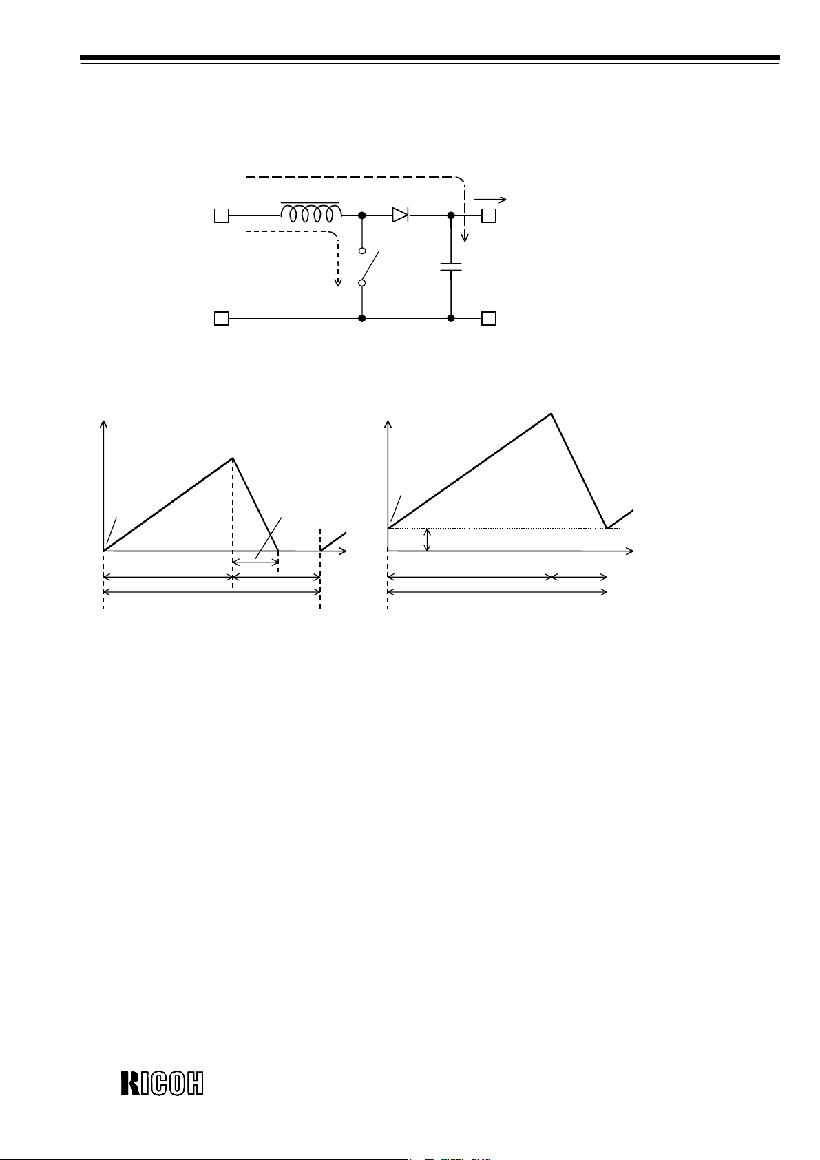
Operation of Step-up DC/DC Converter and Output Current
■
Step-up DC/DC Converter makes higher output voltage than input voltage by releasing the energy accumulated
during on time of Lx Transistor on input voltage.
<Basic Circuit>
i2
OUT
I
OUT
V
C
L
Continuous Mode
ILxmax
IL
ILxmin
IN
V
GND
Discontinuous Mode
ILxmax
Inductor
i1
<Current through L>
Tf
Diode
Lx Tr
IL
ILxmin
Iconst
Ton Toff
T=1/fosc
t
Ton Toff
T=1/fosc
t
Step 1. Lx Tr. is on, then the current IL=i1 flows, and the energy is charged in L. In proportion to the on time of Lx Tr.
(Ton), IL=i1 increases from IL=ILxmin=0 and reaches ILxmax.
Step 2. When the Lx Tr. is off, L turns on Schottky Diode (SD), and IL=i2 flows to maintain IL=ILxmax.
Step 3. IL=i2 gradually decreases, and after Tf passes, IL=ILxmin=0 is true, then SD turns off. Note that in the case of
the continuous mode, before IL=ILxmin=0 is true, Toff passes, and the next cycle starts, then Lx Tr. turns on again.
In this case, ILxmin>0, therefore IL=ILxmin>0 is another starting point and ILx max increases.
With the PWM controller, switching times during the time unit are fixed. By controlling Ton, output voltage is
maintained.
Output Current and Selection of External Components
■
Output Current of Step-up Circuit and External Components
There are two modes, or discontinuous mode and continuous mode for the PWM step-up switching regulator
depending on the continuous characteristic of inductor current.
During on time of the transistor, when the voltage added on to the inductor is described as V
Therefore, the electric power, P
ON
T
PON=∫V
0
2
IN
×
t/L dt Formula 1
ON
, which is supplied with input side, can be described as in next formula.
IN
, the current is V
IN
×
t/L.
With the step-up circuit, electric power is supplied from power source also during off time. In this case, input current is
described as (V
OUT-VIN
)×t/L, therefore electric power, P
OFF
is described as in next formula.
Rev.1.10 - 8 -
 Loading...