How it Works
Log In / Sign Up
Buy Points
How it Works
FAQ
Contact Us
Questions and Suggestions
Users
Datasheet
Loading...
R
R05T0515
R05TR244872
R05U0503
R05U0505
R05U0509
R05U0512
R05U0515
R05V05
R05V09
R05X05
R05X09
R05X12
R05X13
R05X15
R05Y05
R05Y09
R05Y12
R05Y13
R05Y15
R09P05D
R09P09D
R09P12D
R09P15D
R09P1.8D
R09P3.3D
R1080
R10-E2Y4-Q3.2K
R10-E2Y6-V1.5K
R1110N
R1170X
3
R1171x
2
R1172x
2
R1173x
2
R1190x
2
R1200
7
R1200F
6
R1201N
R1201x
R1203x
2
R1204x
R1205x
2
R1210N
R1210Nxx1x
R1210Nxx2x
R1211x
2
R1212D
2
R1213K
2
R1215D
2
R1218x
2
R1224N
2
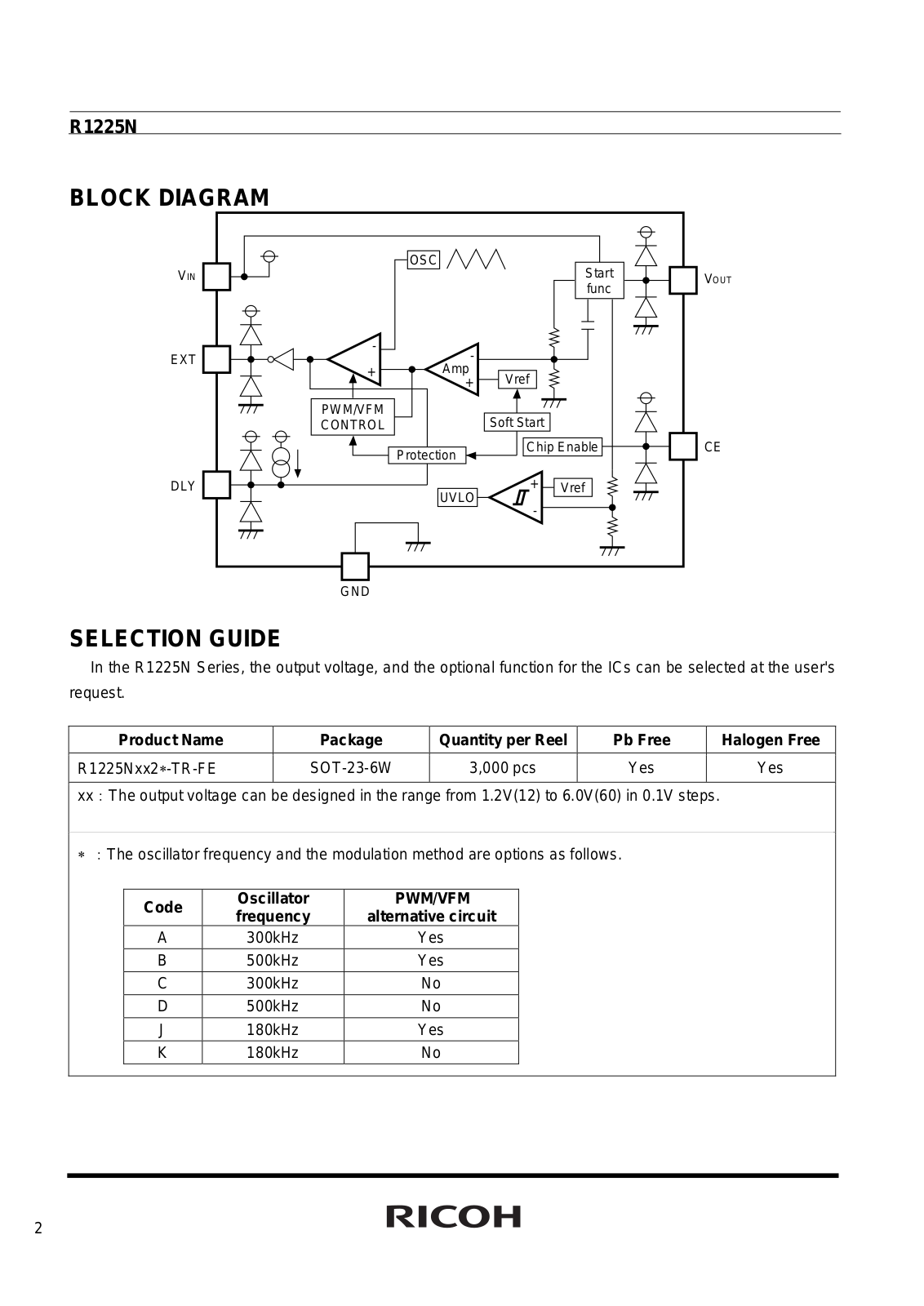
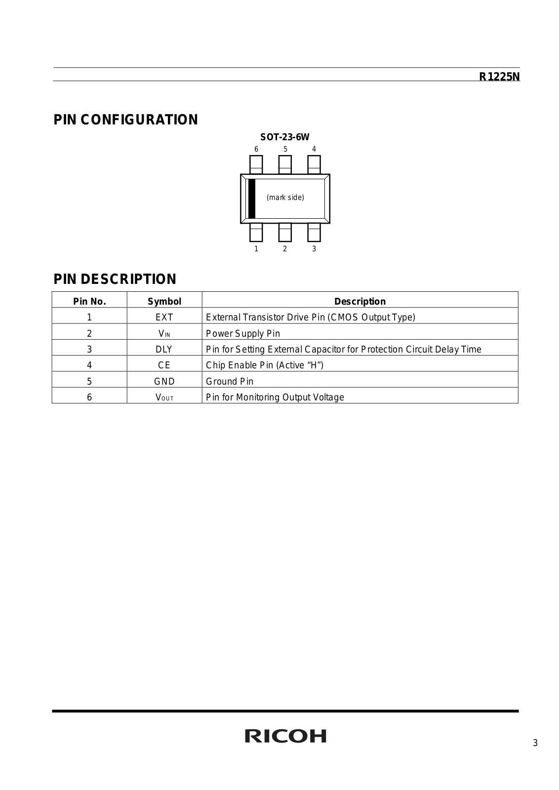
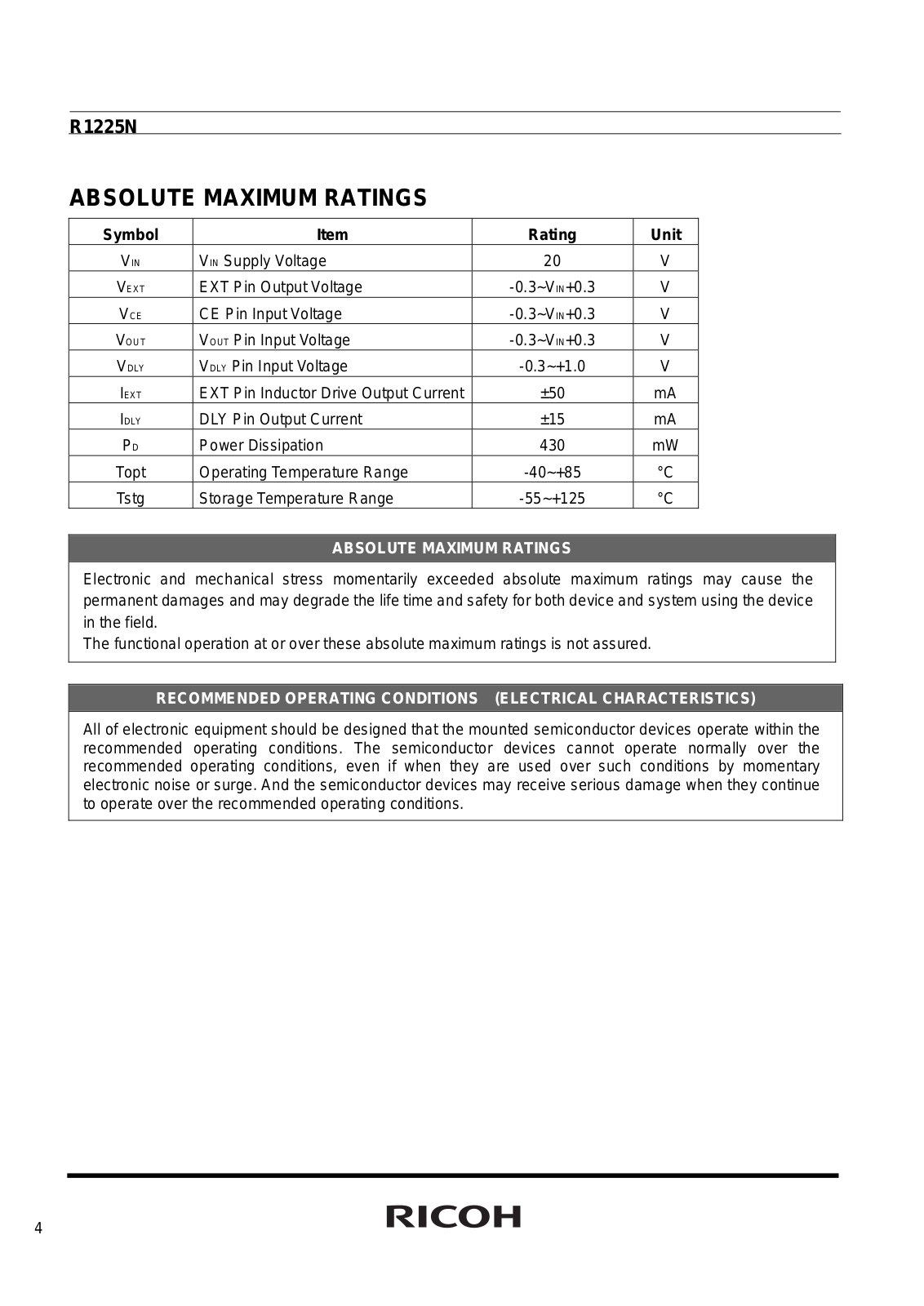
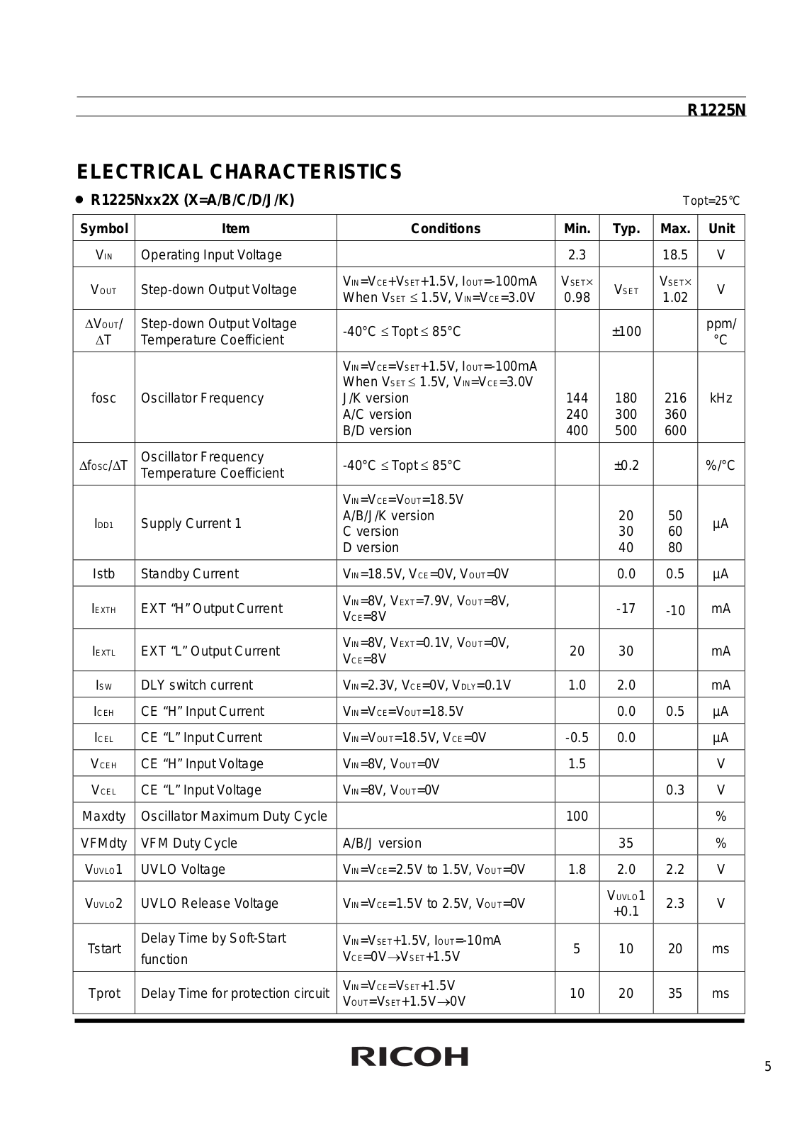
R1225N
2
R1232D
2
R1242S
2
R1243x
2
R1245x
2
R1250
R1250V××1A
R1280D002A-TR
R1280D002B-TR
R1280D002C-TR
R1283K
R1283x
R1286K
2
R1288A
R1290x
R12A05
R12A09
R12A12
R12A15
R12B05
R12B09
R12B12
R12B15
R12C09
R12C12
R12C15
R12D05
R12D09
R12D12
R12D15
R12G05
R12G09
R12G12
R12G15
R12H05
R12H09
R12H12
R12H15
R12I12
R12J05
R12J09
R12J15
R12K05
R12K09
R12K12
R12K15
R12L03
R12L05
R12L09
R12L12
Loading...
Loading...
Nothing found
R1225N
Datasheet (RICOH)
35 pgs
402.07 Kb
0
Datasheet (RICOH)
2 pgs
163.91 Kb
0
Table of contents
Loading...
Datasheet R1225N Datasheet (RICOH)
...
Datasheet Datasheet (RICOH)
Download
Specifications and Main Features
Frequently Asked Questions
User Manual
Download
Loading...
+
hidden pages
Unhide
You need points to download manuals.
1 point = 1 manual.
You can buy points or you can get point for every manual you upload.
Buy points
Upload your manuals


")