How it Works
Log In / Sign Up
Buy Points
How it Works
FAQ
Contact Us
Questions and Suggestions
Users
Datasheet
Loading...
R
R1162N291B
R1162N291D
R1162N301B
R1162N301D
R1162N311B
R1162N311D
R1162N321B
R1162N321D
R1162N331B
R1162N331D
R1162N341B
R1162N341D
R1162N351B
R1162N351D
R1162N361B
R1162N361D
R1162N371B
R1162N371D
R1162N381B
R1162N381D
R1162N391B
R1162N391D
R1162N401B
R1162N401D
R1170X
3
R1171x
2
R1172x
2
R1173x
2
R1178NC14x
R1178NS12x
R1178NS14x
R1190x
2
R1200
7
R1200F
6
R1201N
R1201x
R1203x
2
R1204x
R1205x
2
R1210N
R1210Nxx1x
R1210Nxx2x
R1211NC12x
R1211NS10x
R1211NS12x
R1211x
2
R1212D
2
R1213K
2
R1215D
2
R1218x
2
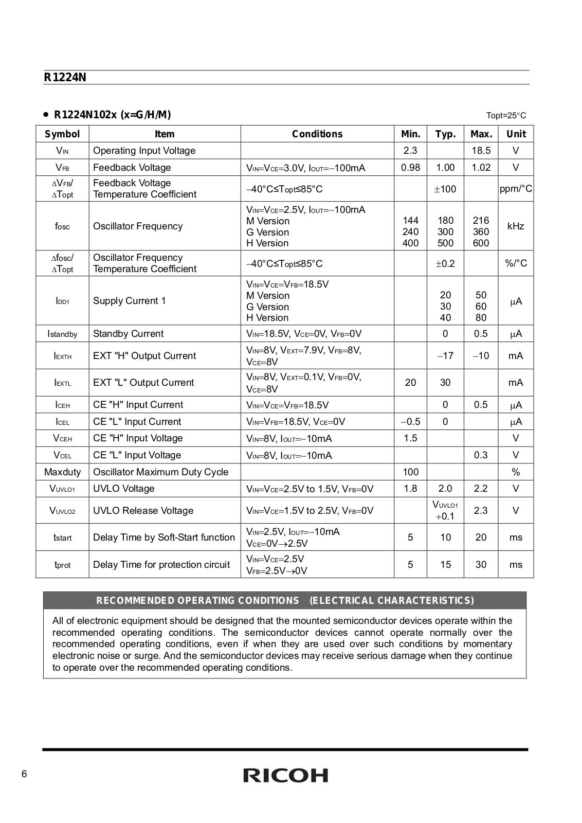
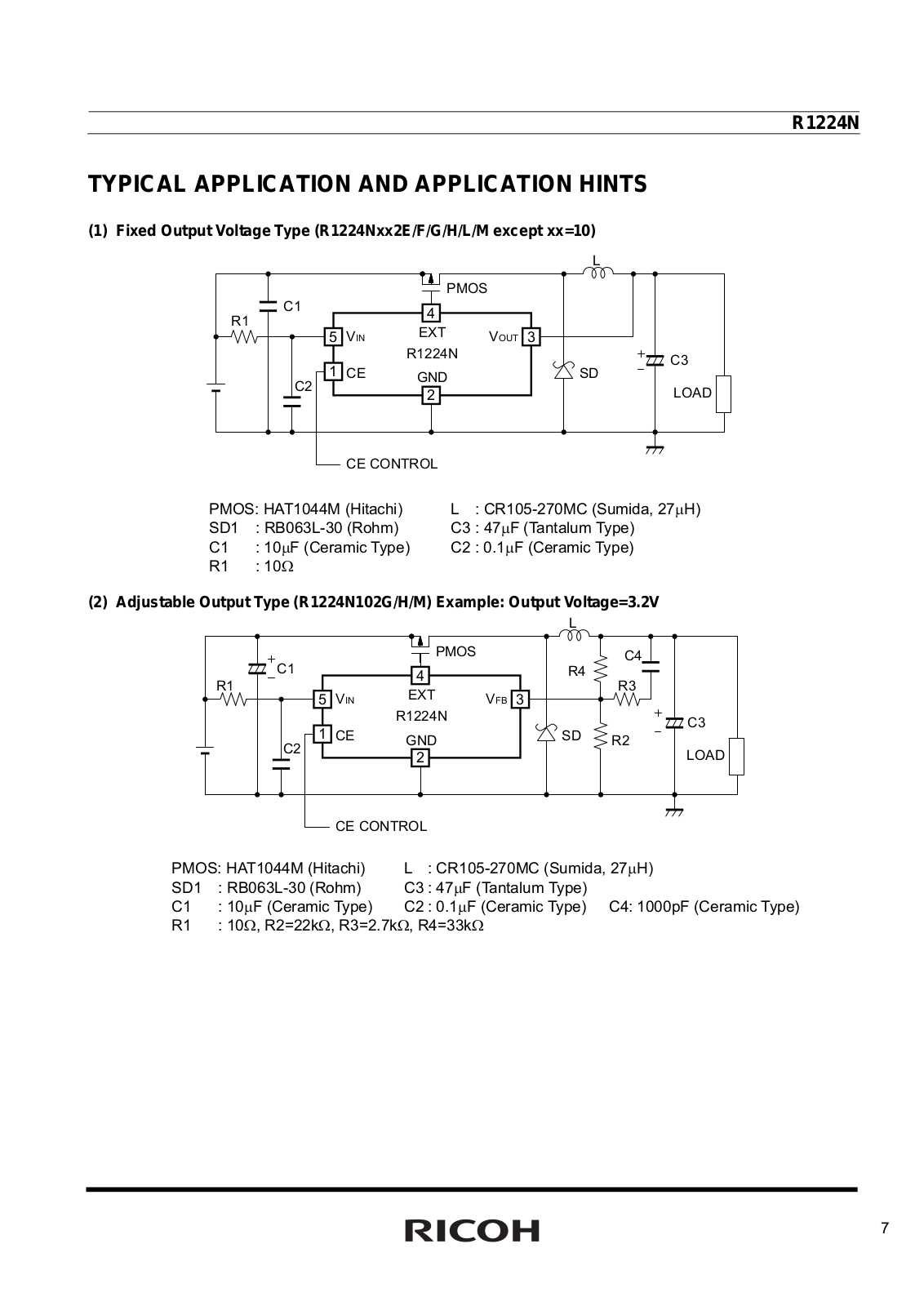
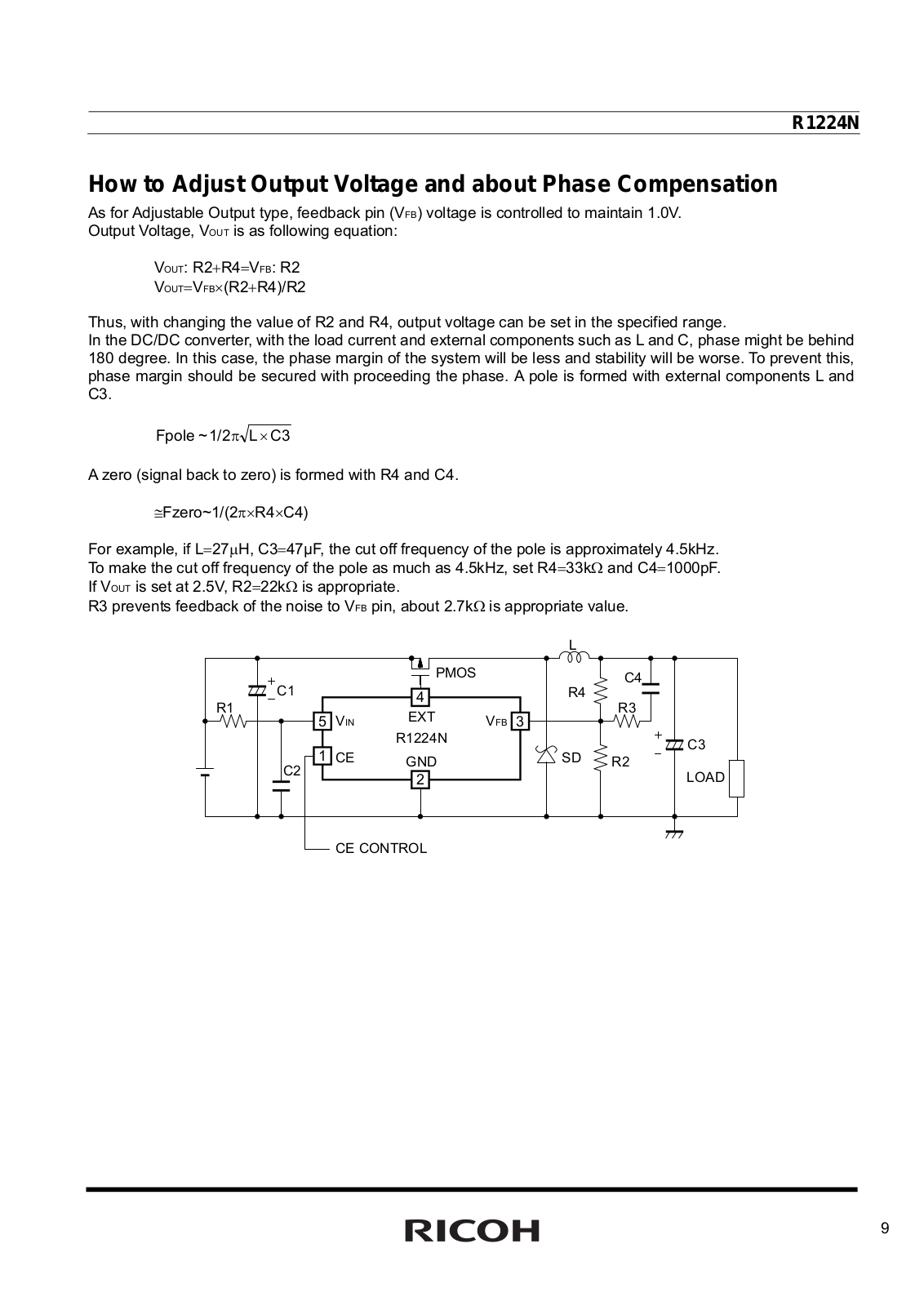
R1224N
2
R1225N
2
R1232D
2
R1242S
2
R1243x
2
R1245x
2
R1250
R1250V××1A
R1271NC12x
R1271NS10x
R1271NS12x
R1275NC14x
R1275NC21x
R1275NS16x
R1275NS21x
R1279NC22x
R1279NC25x
R1279NS22#
R1279NS25#
R1280D002A-TR
R1280D002B-TR
R1280D002C-TR
R1280NC21x
R1280NC25x
R1280NS18#
R1280NS25#
R1283K
R1283x
R1286K
2
R1288A
R1290x
R12A05
R12A09
R12A12
R12A15
R12B05
R12B09
R12B12
R12B15
R12C09
R12C12
R12C15
R12D05
R12D09
R12D12
R12D15
R12G05
R12G09
R12G12
R12G15
Loading...
Loading...
Nothing found
R1224N
Datasheet (RICOH)
40 pgs
466.08 Kb
0
Datasheet (RICOH)
2 pgs
196.2 Kb
0
Table of contents
Loading...
Datasheet R1224N Datasheet (RICOH)
...
Datasheet Datasheet (RICOH)
Download
Specifications and Main Features
Frequently Asked Questions
User Manual
Download
Loading...
+
hidden pages
Unhide
You need points to download manuals.
1 point = 1 manual.
You can buy points or you can get point for every manual you upload.
Buy points
Upload your manuals


")