How it Works
Log In / Sign Up
Buy Points
How it Works
FAQ
Contact Us
Questions and Suggestions
Users
Datasheet
Loading...
R
R0830LS12x
R0830LS14x
R0878LC18x
R0878LC21x
R0878LS16x
R0878LS21x
R0929LC10x
R0929LC12x
R0929LS10x
R0929LS12x
R0964LC10x
R0964LC12x
R0964LS10x
R0964LS12x
R0990LC08x
R0990LS06
R0990LS08
R09P05D
R09P09D
R09P12D
R09P15D
R09P1.8D
R09P3.3D
R1080
R10-E2Y4-Q3.2K
R10-E2Y6-V1.5K
R1110N
R1124NC14x
R1124NC21x
R1124NS16x
R1124NS18x
R1127NC32#
R1127NC36#
R1158NC26x
R1158NS24#
R1158NS26#
R1170X
3
R1171x
2
R1172x
2
R1173x
2
R1178NC14x
R1178NS12x
R1178NS14x
R1190x
2
R1200
7
R1200F
6
R1201N
R1201x
R1203x
2
R1204x
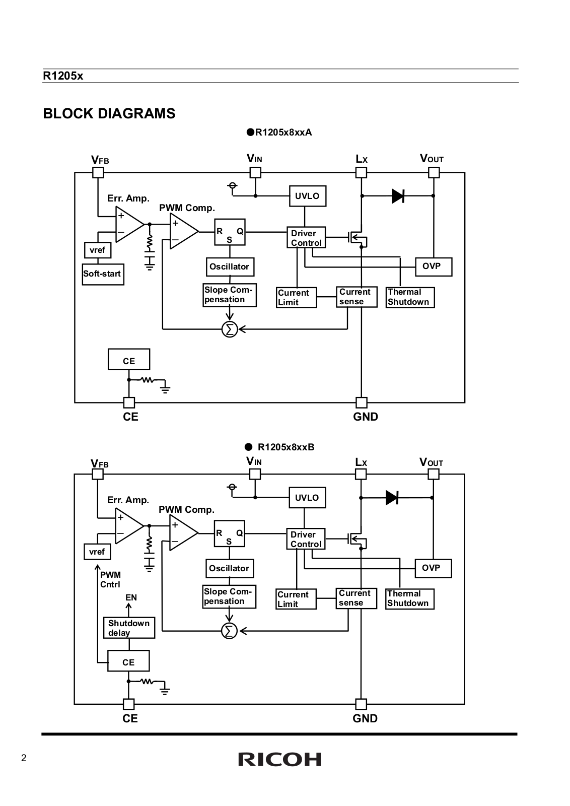
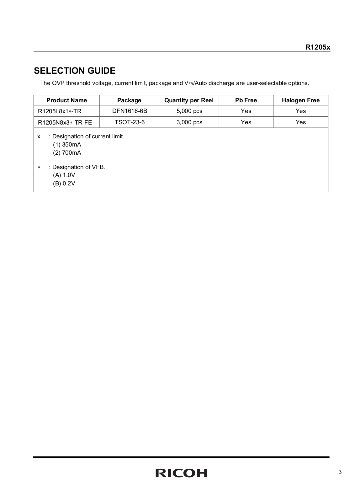
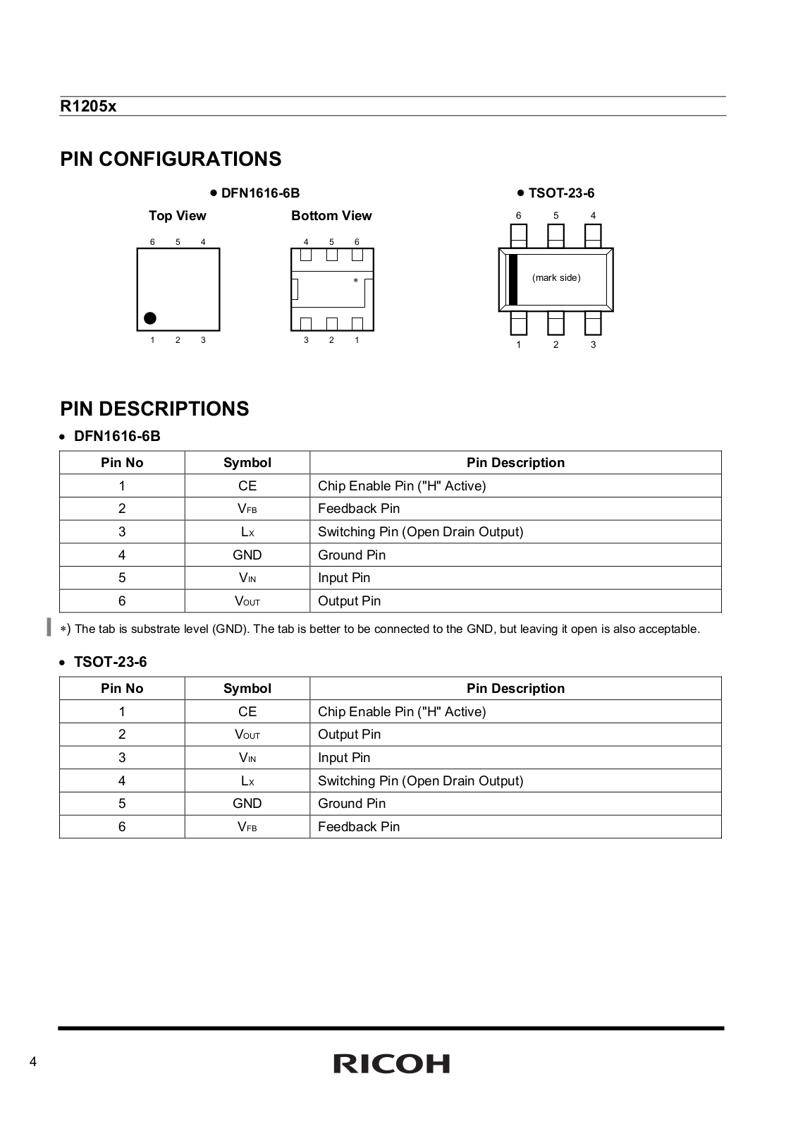
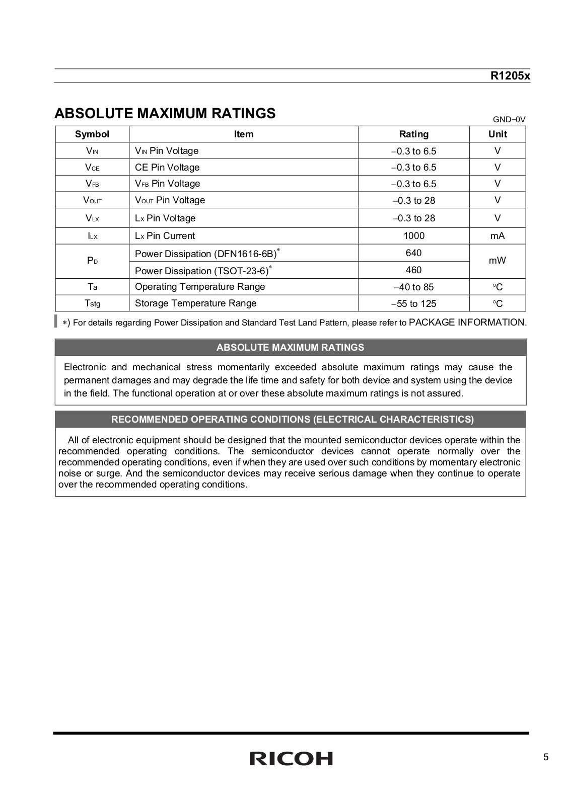
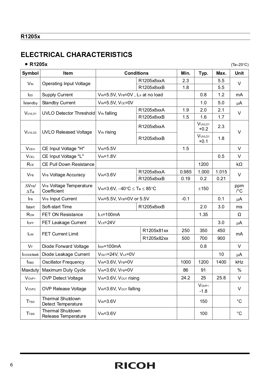
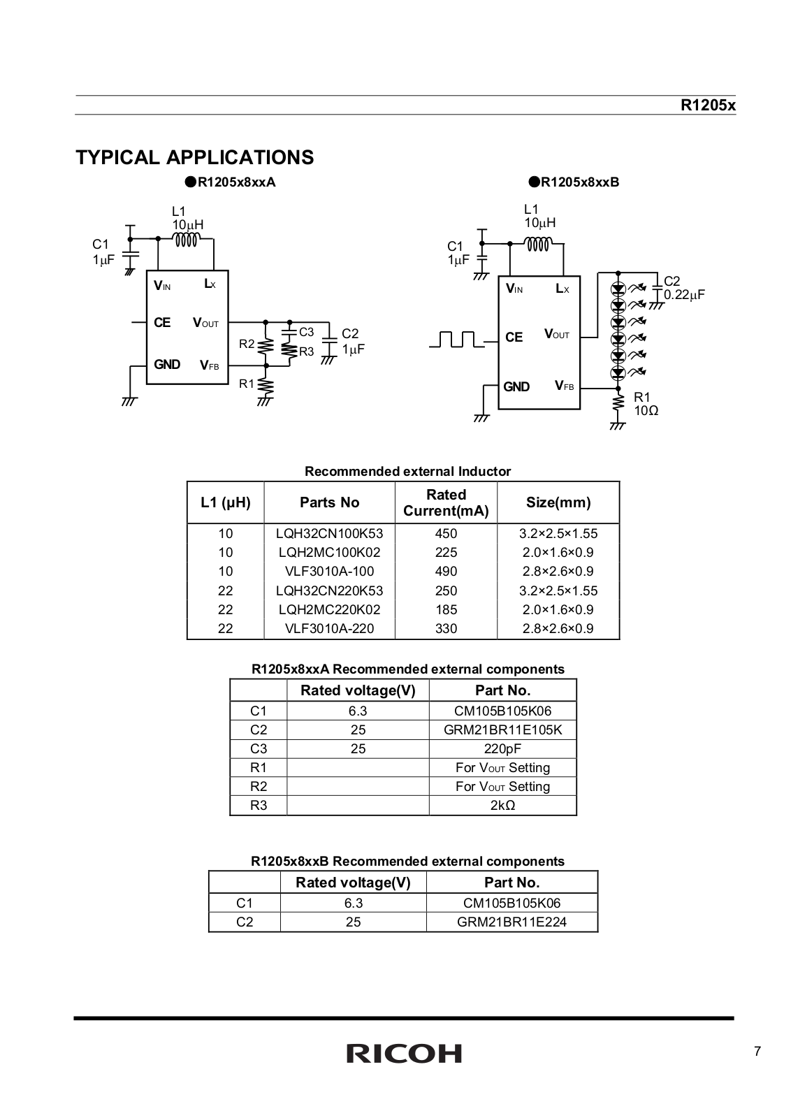
R1205x
2
R1210N
R1210Nxx1x
R1210Nxx2x
R1211NC12x
R1211NS10x
R1211NS12x
R1211x
2
R1212D
2
R1213K
2
R1215D
2
R1218x
2
R1224N
2
R1225N
2
R1232D
2
R1242S
2
R1243x
2
R1245x
2
R1250
R1250V××1A
R1271NC12x
R1271NS10x
R1271NS12x
R1275NC14x
R1275NC21x
R1275NS16x
R1275NS21x
R1279NC22x
R1279NC25x
R1279NS22#
R1279NS25#
R1280D002A-TR
R1280D002B-TR
R1280D002C-TR
R1280NC21x
R1280NC25x
R1280NS18#
R1280NS25#
R1283K
R1283x
R1286K
2
R1288A
R1290x
R12A05
R12A09
R12A12
R12A15
R12B05
R12B09
R12B12
Loading...
Loading...
Nothing found
R1205x
Datasheet (RICOH)
21 pgs
498.02 Kb
0
Datasheet (RICOH)
2 pgs
309.07 Kb
0
Table of contents
Loading...
Datasheet R1205x Datasheet (RICOH)
...
Datasheet Datasheet (RICOH)
Download
Specifications and Main Features
Frequently Asked Questions
User Manual
Download
Loading...
+
hidden pages
Unhide
You need points to download manuals.
1 point = 1 manual.
You can buy points or you can get point for every manual you upload.
Buy points
Upload your manuals


")