How it Works
Log In / Sign Up
Buy Points
How it Works
FAQ
Contact Us
Questions and Suggestions
Users
RICOH
Loading...
R
R1162N181D5
R1162N191B
R1162N191D
R1162N201B
R1162N201D
R1162N211B
R1162N211D
R1162N221B
R1162N221D
R1162N231B
R1162N231D
R1162N241B
R1162N241D
R1162N251B
R1162N251D
R1162N261B
R1162N261D
R1162N271B
R1162N271D
R1162N281B
R1162N281B5
R1162N281D
R1162N291B
R1162N291D
R1162N301B
R1162N301D
R1162N311B
R1162N311D
R1162N321B
R1162N321D
R1162N331B
R1162N331D
R1162N341B
R1162N341D
R1162N351B
R1162N351D
R1162N361B
R1162N361D
R1162N371B
R1162N371D
R1162N381B
R1162N381D
R1162N391B
R1162N391D
R1162N401B
R1162N401D
R1162x
R1163x
2
R1170X
3
R1171x
2
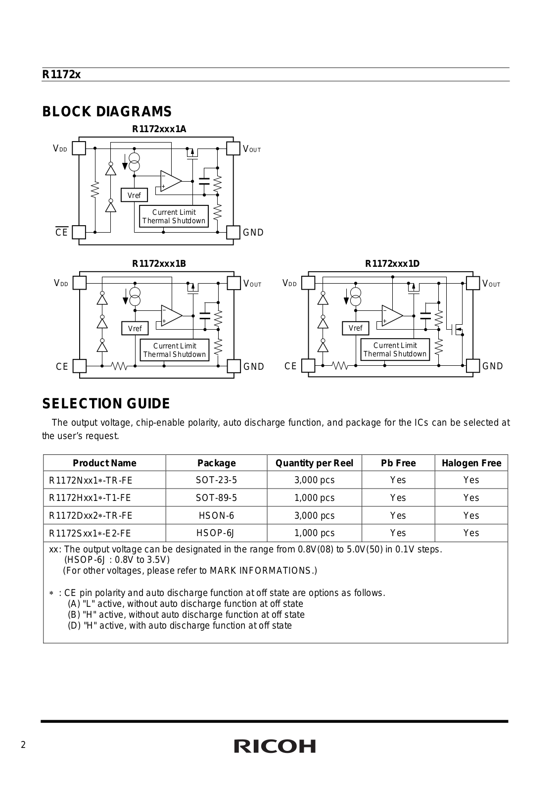
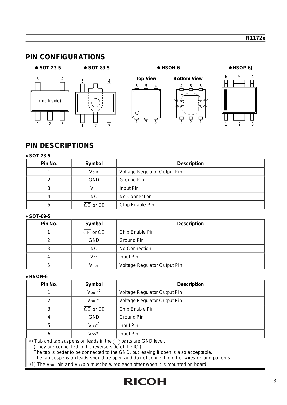
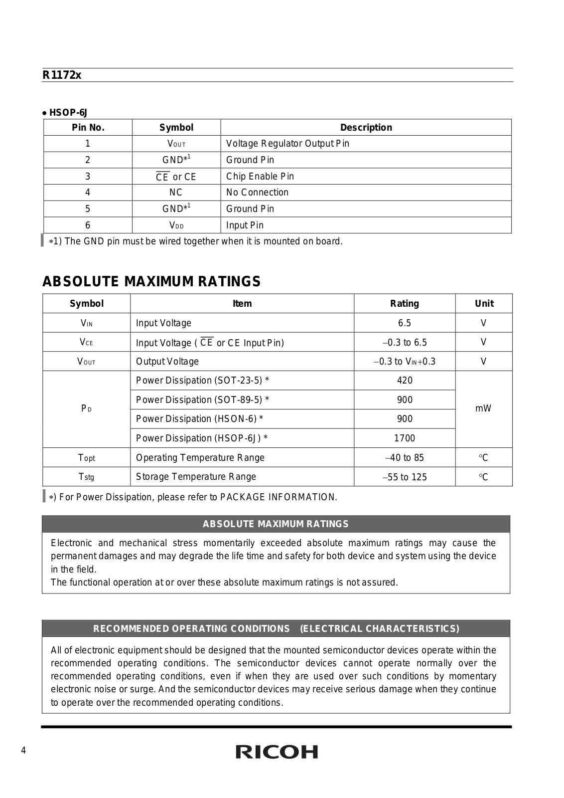
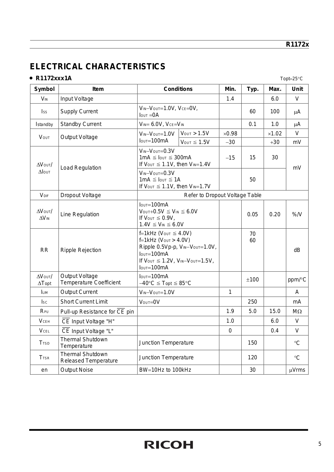
R1172x
2
R1173x
2
R1180x
2
R1182x
2
R1183Z
R1190x
2
R1191x
R1200x
2
R1201N
R1201x
R1202x
R1203x
2
R1204x
2
R1205x
2
R1210N
R1210Nxx1x
R1210Nxx2x
R1211x
2
R1212D
2
R1213K
2
R1215D
2
R1218x
2
R1224N
2
R1225N
2
R1232D
2
R1242S
2
R1243x
2
R1245x
2
R1250V××1A
R1280D002A-TR
R1280D002B-TR
R1280D002C-TR
R1283K
R1283x
R1286K
2
R1290x
R1500x
2
R1501x
2
R1510S
2
R1514x
2
R1515x
2
R1516x
R1v
9
R2
8
R2023K
R2023T
R2025D
R2025S
R2033K
R2033T
Loading...
Loading...
Nothing found
R1172x
Technical data
25 pgs
524.64 Kb
0
Technical data
2 pgs
248.91 Kb
0
Table of contents
Loading...
RICOH R1172x Technical data
...
RICOH Technical data
Download
Specifications and Main Features
Frequently Asked Questions
User Manual
Download
Loading...
+
17
hidden pages
Unhide
You need points to download manuals.
1 point = 1 manual.
You can buy points or you can get point for every manual you upload.
Buy points
Upload your manuals
 Loading...