

Page 1

7 CH Power Management IC
RT9971
General Description
The RT9971 is a complete power supply solution for digital
still cameras and other hand held devices. The RT9971 is
a multi-channel power management IC including two stepup DC/DC converters, two step-down DC/DC converters,
one selectable step-up/step-down DC/DC converter, one
inverting DC/DC converter and one WLED driver.
The RT9971 is designed to fulfill the applications for DSC
just as follows :
CH1 is a synchronous step-up output for motor or DSC
system I/O power
CH2 is a selectable synchronous step-up/step-down
output for motor or DSC system I/O power
CH3 and CH4 are synchronous step-down outputs for DSP
core and memory power supply
CH5 is a high voltage step-up output for CCD bias power
supply
CH6 is an inverting output for negative CCD bias power
supply
CH7 is a high voltage step-up output for driving WLED
Features
l One Synchronous Step-Up or Step-Down
Selectable Convertor
l Support 2AA or Li-ion Battery Applications
l Preset On/Off Sequence
l 5 CHs with Internal Compensation
l All Power Switches Integrated
l Up to 95% Efficiency
l 100% (max) Duty Cycle for Step-Down Converter
l Adjustable Output Voltage
l LED PWM Dimming Control
l LED Open Protection
l Transformerless Inverting Converter for CCD
l Fixed 1MHz Switching Frequency at CH1 to CH7
l RTC_LDO/SW1 Selectable by CN Pin
l 40-Lead WQFN Package
l RoHS Compliant and Halogen Free
Applications
l Digital Still Camera
l PDA
l Portable Device
For the CH2, the step-up or step-down converter, operation
mode can be selected by the SEL pin. Among all CHs,
there are 5 CHs with the built-in internal compensation.
The RT9971 also provides a transformerless inverting
converter for supplying the CCD power. For the
synchronous step-up and step down converters, the
efficiency can be up to 95%. The IC provides load
disconnection for CH 1 and CH 5. The IC has selectable
RTC_LDO/SW1 that can be determined by the CN pin.
The RT9971 is able to support Li-ion and 2AA battery
applications. The RT9971 provides WLED open protection,
current limit, thermal shutdown protection, over voltage
and under voltage protection to achieve complete
protection. The RT9971 is available in WQFN-40L 5x5
package.
Ordering Information
RT9971
Package Type
QW : WQFN-40L 5x5 (W-Type)
Lead Plating System
G : Green (Halogen Free and Pb Free)
Note :
Richtek products are :
} RoHS compliant and compatible with the current require-
ments of IPC/JEDEC J-STD-020.
} Suitable for use in SnPb or Pb-free soldering processes.
DS9971-01 April 2011 www.richtek.com
1
Page 2

RT9971
Pin Configurations
PVDD1
LX6
PVDD6
CP
CN
PNEG
FB6
FB4
EN6
LX4
(TOP VIEW)
EN2
COMP1
LX1
40
1
2
3
4
5
6
7
8
9
10
11
PVDD4
FB1OKVOUT1
39
EN5
SW5I
SW5O
GND
FB5
FB2
COMP2
EN134
LX2
35363738
34
VREF
313233
30
PVDD2
29
VDDM
28
CFB7
27
GND
26
LX7
25
LX5
24
VOUT7
FB3
23
41
22
EN7
21
LX3
201918171615141312
SEL
RTC_R
PVDD3
RTC_PWR
WQFN-40L 5x5
DS9971-01 April 2011www.richtek.com
2
Page 3

Typical Application Circuit
→
→→→→→
For 2AA
V
V
OUT_SW1
V
3.3V
OUT_CH2
3V3
3V3
BAT
V
OUT_CH1
C5
10µFx2
V
OUT_CH3
2.5V
V
OUT_CH4
1.8V
R19
50k
10µF
C12
10µF
V
C9
BAT
3V3
470k
R4
470k
R5
88.7k
Q1
C1
10µF
5V
C8
10uF
C11
10uF
R1
R2
150k
10µF
R7
768k
R8
360k
R9
470k
R10
374k
C2
4.7pF
C4
C6
4.7pF
C22
10µF
C3
560pF
C7
560pF
OFF
L22.2µH
C10
C13
33pF
ON
V
L1
2.2µH
10µF x 2
R3
39k
R6
39k
4.7µH
22pF
4.7µH
BAT
C27
L3
L4
40
37
38
36
35
31
30
34
33
20
21
23
11
10
39
32
12
17
22
1
8
9
LX1
PVDD1
FB1
COMP1
OK
VOUT1
LX2
PVDD2
FB2
COMP2
PVDD3
LX3
FB3
PVDD4
LX4
FB4
EN2
EN134
EN5
EN6
SEL
EN7
3V3
29
VDDM
RT9971
C23
1µF
SW5O
SW5I
PVDD6
VREF
VOUT7
CFB7
RTC_R
RTC_PWR
PNEG
GND
V
BAT
25
LX5
13
14
15
FB5
3
C25
1µF
2
LX6
7
FB6
16
26
LX7
24
28
18
19
4
CP
5
CN
6
27, Exposed Pad (41)
L5
10µH
D3
D4
R16
10k
C29
1µF
L6
10µH
10µH
C28
0.1µF
D5
C24
1µF
C14
10µF/25V
C15
1nF
V
BAT
R13
63.4k
R14
11.3k
L7
RTC Reset
RTC 3.25V
C26
1µF
15V
R11
1000k
R12
90.9k
RT9971
C16
10µF/25V
V
-7V
C18
C17
10µF/16V x 2
1nF
C19
0.1µF
D1
C20
D2
1µF/16V
R15
10
V
OUT_CH5
15V
OUT_CH6
V
BAT
WLED
Note :
(1) SEL = High, CH2 is Step -Up, CN Connect to CAP
(2) V
= 1.8V to 3.2V
BAT
Timing Diagram
Power On Sequence : CH1 Step -Up 3.3V CH3 Step -Down 2.5V CH4 Step -Down 1.8V (CH2 Step -Up 5V and
SW1 3.3V)
Power Off Sequence : (CH2 Step -Up 5V and SW1 3.3V) CH4 Step -Down 1.8V CH3 Step -Down 2.5V CH1
Step -Up 3.3V
VDDM
EN2, EN134
V
V
V
V
OUT_CH1
OUT_CH3
OUT_CH4
OUT_SW1
V
OUT_CH2
3.3V
2.5V
1.8V
3.3V
5V
DS9971-01 April 2011 www.richtek.com
User define
3.5ms
3.5ms
3.5ms
3.5ms
3.5ms
IC shutdown
Wait until FB3 < 0.1V
Wait until FB4 < 0.1V
Wait until V
OUT1
< 0.4V
Depends on loading
3
Page 4

RT9971
→→→→→
→
For Li-ion
V
OUT_CH1
5V
RTC 3.25V
V
BAT
or 5V
V
BAT
V
BAT
C1
10µF x 2
V
C4
10µF
C8
10µF
C11
10µF
OUT_CH2
3.3V
C5
10µF
V
OUT_CH3
2.5V
10µF
V
OUT_CH4
1.8V
10µF
C9
C12
V
R1
470k
R2
88.7k
BAT
R4
470k
R5
150k
R7
768k
R8
360k
R9
470k
R10
374k
C2
4.7pF
560pF
C3
OFF
C22
10µF
C21
0.22F
C6
10pF
2200pF
C7
C10
22pF
C13
33pF
ON
L1
2.2µH
R3
39k
V
BAT
L2
4.7µH
4.7µH
4.7µH
L3
L4
R6
15k
40
37
38
36
35
30
31
34
33
20
21
23
11
10
39
32
12
17
22
1
8
9
LX1
PVDD1
FB1
COMP1
OK
VOUT1
PVDD2
LX2
FB2
COMP2
PVDD3
LX3
FB3
PVDD4
LX4
FB4
EN2
EN134
EN5
EN6
SEL
EN7
V
BAT
29
VDDM
RT9971
C23
1µF
SW5O
SW5I
PVDD6
VREF
VOUT7
CFB7
RTC_R
RTC_PWR
PNEG
V
25
LX5
13
14
15
FB5
3
2
LX6
7
FB6
16
26
LX7
24
28
18
19
4
CP
5
CN
6
27, Exposed Pad (41)
GND
BAT
C25
1µF
L5
10µH
D3
D4
R16
10k
10µH
R18
10k
V
L6
10µH
C24
1µF
C14
10µF/25V
C15
1nF
BAT
L7
D5
RTC Reset
RTC 3.25V
R13
63.4k
R14
11.3k
V
BAT
C26
1µF
15V
R11
1000k
R12
90.9k
C17
1nF
10
D1
D2
R15
C19
0.1µF
C16
10uF/25V
C18
10µF/16V x 2
C20
1µF/16V
V
OUT_CH5
15V
V
OUT_CH6
-7V
V
BAT
WLED
Note :
(1) SEL = Low, CH2 is Step -Down, CN Pull High
(2) V
= 2.7V to 4.2V
BAT
Timing Diagram
Power On Sequence : CH1 Step -Up 5V CH3 Step -Down 2.5V CH4 Step -Down 1.8V CH2 Step -Down 3.3V
Power Off Sequence : CH2 Step -Down 3.3V CH4 Step -Down 1.8V CH3 Step -Down 2.5V CH1 Step -Up 5V
VDDM
EN2, EN134
V
V
OUT_CH3
V
OUT_CH4
V
OUT_CH2
OUT_CH1
5V
2.5V
1.8V
3.3V
4
User define
3.5ms
3.5ms
3.5ms
3.5ms
IC shutdown
Wait until FB3 < 0.1V
Wait until FB4 < 0.1V
Wait until FB2 < 0.1V
DS9971-01 April 2011www.richtek.com
Page 5

Table 1. Recommended Components for the Typical Application Circuit
Channel CH3
RT9971
Formula V
V
OUT_CH3
(V) 2.5 1.8 1.5 1.3 1.2 1
OUT_CH3
= (1+R7/R8) x 0.8
L3 (µH) 4.7 4.7 4.7 4.7 4.7 4.7
R7 (kΩ) 768 470 330 237 187 23.2
R8 (kΩ) 360 374 374 374 374 93.1
C10 (pF) 22 33 47 68 82 47
C9 (µF) 10 10 10 10 10 10
Channel CH4
Application V
V
OUT_CH4
(V) 2.5 1.8 1.5 1.3 1.2 1
OUT_CH4
= (1+R9/R10) x 0.8
L4 (µH) 4.7 4.7 4.7 4.7 4.7 4.7
R9 (kΩ) 768 470 330 237 187 23.2
R10 (kΩ) 360 374 374 374 374 93.1
C13 (pF) 22 33 47 68 82 47
C12 (µF) 10 10 10 10 10 10
Channel CH5
Formula V
V
OUT_CH5
(V) 12 13 14 15 15.5 16
OUT_CH5
= (1+R11/R12) x 1.25
L5 (µH) 10 10 10 10 10 10
R11 (kΩ) 820 820 953 1000 820 886
R12 (kΩ) 95.3 86.6 93.1 90.9 71.5 75
C15 (pF) 1000 1000 1000 1000 1000 1000
C16 (µF) 10/16V 10/16V 10/25V 10/25V 10/25V 10/25V
Channel CH6
Formula V
V
OUT_CH6
(V) -6 -6.3 -7 -7.5 -8
OUT_CH6
= (R13/R14) x (-1.25) * R13+R14 <90k
L6 (µH) 10 10 10 10 10
R13 (kΩ) 57.6 69.8 63.4 68 68
R14 (kΩ) 12 13.7 11.3 11.3 10.5
C17 (pF) 1000 1000 1000 1000 1000
C18 (µF) 10 x 2pcs. 10 x 2pcs. 10 x 2pcs. 10 x 2pcs. 10 x 2pcs.
DS9971-01 April 2011 www.richtek.com
5
Page 6

RT9971
oltage. High impedance
. High impedance in
Functional Pin Description
Pin No. Pin Name Pin Function
1 PVDD1 Power Output of CH1.
2 LX6 Switch Node of CH6. High impedance in shutdown mode.
3 PVDD6 Power Input of CH6.
4 CP Charge Pump External Driver.
5 CN Charge Pump External Driver.
6 PNEG Negative Output of Charge Pump.
7 FB6 Feedback Input of CH6. High impedance in shutdown mode.
8 FB4 Feedback Input of CH4. High impedance in shutdown mode.
9 EN6 Enable Control Input of CH6.
10 LX4 Switch Node of CH4. High impedance in shutdown mode.
11 PVDD4 Power Input of CH4.
12 EN5 Enable Control Input of CH5.
13 SW5O Output of CH5 Load Disconnect.
14 SW5I Input of CH5 Load Disconnect.
15 FB5 Feedback Input of CH5. High impedance in shutdown mode.
16 VREF 1.25V Reference Output.
17 SEL Li-ion or 2AA Select. Logic state can not be changed during operation.
18 RTC_R RTC_Reset Output.
19 RTC_PWR Power Input of RTC_Reset.
20 PVDD3 Power Input of CH3.
21 LX3 Switch Node of CH3. High impedance in shutdown mode.
22 EN7 Enable Control Input of CH7.
23 FB3 Feedback Input of CH3. High impedance in shutdown mode.
24 VOUT7 Sense Input for CH7 Output Voltage.
25 LX5 Switch Node of CH5. High impedance in shutdown mode.
26 LX7 Switch Node of CH7. High impedance in shutdown mode.
27,
41 (Exposed Pad)
28 CFB7 Feedback Input of CH7.
29 VDDM IC Analog Power Input.
30 PVDD2
31 LX2 Switch Node of CH2. High impedance in shutdown mode.
32 EN134 Enable Control Input of CH1, CH3 and CH4.
33 COMP2 Compensation of CH2. Pull to GND in shutdown mode.
34 FB2 Feedback input of CH2. High impedance in shutdown mode.
35 VOUT1
36 OK
37 FB1 Feedback Input of CH1. High impedance in shutdown mode.
38 COMP1 Compensation of CH1. Pull to GND in shutdown mode.
39 EN2 Enable Control Input of CH2.
40 LX1 Switch Node of CH1. High impedance in shutdown mode.
6
GND
Ground. The exposed pad must be soldered to a large PCB and connected to
GND for maximum thermal dissipation.
Power Input of CH2 step-down converter, or power output of CH2 step-up
converter.
CN is set to low or floating : Sense Pin for CH1 Output V
in shutdown. CN is set to High: Output pin of RTC_LDO.
CN is set to low or floating : External Switch Control
shutdown. CN is set to High : Power input pin of RTC_LDO.
DS9971-01 April 2011www.richtek.com
Page 7

Function Block Diagram
RT9971
VDDM
LX5
FB5
SW5I
SW5O
PVDD6
LX6
FB6
LX7
VOUT7
EN7
CFB7
VREF
EN2
EN134
EN5
EN6
SEL
CP
CN
PNEG
OK
VOUT1
1.25V
REF
0.25V
REF
1.25V
REF
SW1
+
+
-
-
+
CH5
C-Mode
Step-Up
PWM
CH6
C-Mode
Inverting
CH7
C-Mode
Step-Up
PWM
Sequence
Negative
Charge
Pump
RTC
LDO
SW5
VDDM
Enable
Mode
CH1
C-Mode
Step-Up
CH2
C-Mode
Step-Up or
Step-Down
CH3
C-Mode
Step-Down
CH4
C-Mode
Step-Down
PVDD1
LX1
+
0.8V
REF
+
0.8V
REF
+
0.8V
REF
COMP1
FB1
PVDD2
LX2
COMP2
FB2
PVDD3
LX3
FB3
PVDD4
LX4
RTC_PWR
RTC_R
RTC
Reset
GND
+
0.8V
REF
FB4
Timing Diagram
CH5 and CH6 Timing Diagram
DS9971-01 April 2011 www.richtek.com
EN5
SW5I
SW5O
(to CCD +)
EN6
V
OUT_CH6
(to CCD -)
10ms
10ms
Depends on loading
Depends on loading
Depends on loading
7
Page 8
RT9971
Absolute Maximum Ratings (Note 1)
l Supply Voltage, V
l Power Switch :
------------------------------------------------------------------------------ −0.3V to 7V
DDM
LX1, LX2, LX3, LX4---------------------------------------------------------------------------------- −0.3V to 6.5V
LX5, LX7, SW5I, SW5O, VOUT7---------------------------------------------------------------- −0.3V to 21V
LX6-----------------------------------------------------------------------------------------------------(PVDD6 − 14V) to (PVDD6 + 0.3V)
l The Other Pins-------------------------------------------------------------------------------------- −0.3V to 6.5V
l Power Dissipation, P
@ T
D
= 25°C
A
WQFN 40L 5x5--------------------------------------------------------------------------------------2.778W
l Package Thermal Resistance (Note 2)
WQFN 40L 5x5, θJA---------------------------------------------------------------------------------36°C/W
WQFN 40L 5x5, θJC--------------------------------------------------------------------------------7°C/W
l Junction Temperature------------------------------------------------------------------------------150°C
l Lead Temperature (Soldering, 10 sec.)---------------------------------------------------------260°C
l Storage Temperature Range---------------------------------------------------------------------- −65°C to 150°C
l ESD Susceptibility (Note 3)
HBM (Human Body Mode)------------------------------------------------------------------------2kV
MM (Machine Mode)-------------------------------------------------------------------------------200V
Recommended Operating Conditions (Note 4)
l Junction Temperature Range--------------------------------------------------------------------- −40°C to 125°C
l Ambient Temperature Range--------------------------------------------------------------------- −40°C to 85°C
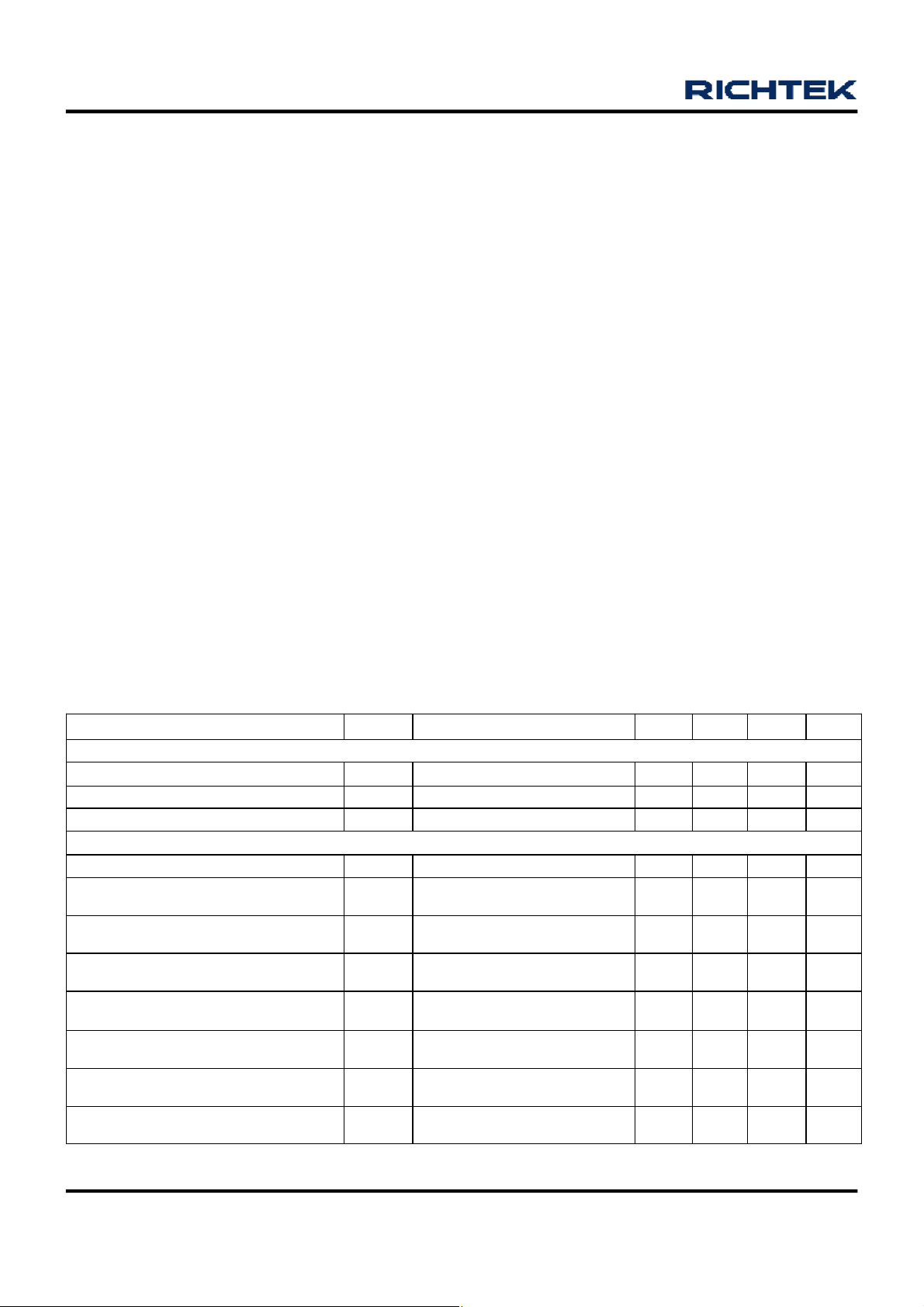
Electrical Characteristics
(V
= 3.3V, T
DDM
Supply Voltage
VDDM Operating Voltage V
VDDM Startup Voltage VST 1.5 -- -- V
VDDM Over Voltage Protection 6 6.25
Supply Current
Shutdown Supply Current into VDDM I
CH1 (Syn-Step-Up) : Supply Current
into VDDM
CH2 (Syn-Step-Up or Syn-Step-Down)
: Supply Current into VDDM
CH3 (Syn-Step-Down) :
Supply Current into VDDM
CH4 (Syn-Step-Down) :
Supply Current into VDDM
CH5 (Asyn-Step-Up) :
Supply Current into VDDM
CH6 (Inverting) + Charge pump :
Supply Current into VDDM
CH7 (WLED):
Supply Current into VDDM
= 25°C, unless otherwise specified)
A
Parameter Symbol
2.7 -- 5.5 V
DDM
All EN = 0, CN = 3.3V -- 5 10 µA
OFF
IQ1 Non Switching, EN134 = 3.3V
IQ2 Non Switching, EN2 = 3.3V -- -- 800 µA
IQ3 Non Switching, EN134 = 3.3V
IQ4 Non Switching, EN134 = 3.3V
IQ5 Non Switching, EN5 = 3.3V -- -- 800 µA
IQ6
IQ7 Non Switching, EN7 = 3.3V -- -- 800 µA
Test Condition Min Typ Max Unit
Non Switching, EN6 = 3.3V
PVDD6 = 3.3V
6.5 V
-- -- 800 µ A
-- -- 800 µ A
-- -- 800 µ A
-- -- 800 µ A
To be continued
DS9971-01 April 2011www.richtek.com
8
Page 9

RT9971
Parameter Symbol
Test Condition Min Typ Max Unit
Oscillator
CH1,2,3,4, 5, 6, 7 Operating Frequency f
CH1 Maximum Duty Cycle (Step-Up) V
CH2 Maximum Duty Cycle (Step-Up) V
CH2 Maximum Duty Cycle (Step-Down) V
CH3 Maximum Duty Cycle (Step-Down) V
CH4 Maximum Duty Cycle (Step-Down) V
CH5 Maximum Duty Cycle (Step-Up) V
CH6 Maximum Duty Cycle (Inverting) V
CH7 Maximum Duty Cycle (WLED) V
900 1000 1100 kHz
OSC
= 0.7V 80 83 86 %
FB1
= 0.7V 80 83 86 %
FB2
= 0.7V -- -- 100
FB2
= 0.7V -- -- 100
FB3
= 0.7V -- -- 100
FB4
= 1.15V 91 94 97 %
FB5
= 0.1V 91 94 97 %
FB6
= 0.15V 91 94 97 %
FB7
%
%
%
Feedback Regulation Voltage
Feedback Regulation Voltage @ FB1,
FB2, FB3, FB4
0.788 0.8 0.812 V
Feedback Regulation Voltage @ FB5 1.237 1.25 1.263 V
Feedback Regulation Voltage @ FB6
(Inverting)
Feedback Regulation Voltage @ CFB7
-15 0 15 mV
0.237 0.25 0.263 V
OK Sink Current OK = 1V 50 -- -- µA
Reference
VREF Output Voltage V
VREF Load Regulation 0µA < I
1.237 1.25 1.263 V
REF
< 200µA -- -- 10 mV
REF
Negative Charge Pump
PVDD6 Low Threshold to Start Pump 3.4 3.6 3.8 V
PVDD6 Hysteresis Gap to Stop Pump 0.1 0.3 0.5 V
(PVDD6 − PNEG) Clamped Voltage PVDD6 = 3.3V 4.1 4.5 4.9 V
Power Switch
CH1 On Resistance of MOSFET R
DS(ON)
P-MOSFET, PVDD1 = 3.3V
N-MOSFET, PVDD1 = 3.3V
-- 150 --
-- 150 --
mΩ
CH1 Current Limitation (Step-Up) -- 3 -- A
CH2 On Resistance of MOSFET R
DS(ON)
P-MOSFET, PVDD2 = 3.3V
N-MOSFET, PVDD2 = 3.3V
-- 150 --
-- 150 --
mΩ
CH2 Current Limitation (Step-Down) -- 1.5 -- A
CH2 Current Limitation (Step-Up) -- 3 -- A
CH3 On Resistance of MOSFET R
DS(ON)
P-MOSFET, PVDD3 = 3.3V
N-MOSFET, PVDD3 = 3.3V
-- 200 --
-- 200 --
mΩ
CH3 Current Limitation (Step-Down) -- 1.5 -- A
CH4 On Resistance of MOSFET R
DS(ON)
P-MOSFET, PVDD4 = 3.3V
N-MOSFET, PVDD4 = 3.3V
-- 200 --
-- 200 --
mΩ
CH4 Current Limitation (Step-Down) -- 1.5 -- A
CH5 Load Disconnect MOSFET P-MOSFET, SW5I = 3.3V -- 0.5 -- Ω
CH5 On Resistance of MOSFET
N-MOSFET -- 0.5 -- Ω
CH5 Current Limitation N-MOSFET -- 1.2 -- A
To be continued
DS9971-01 April 2011 www.richtek.com
9
Page 10

RT9971
Parameter Symbol
CH6 On Resistance of MOSFET P-MOSFET, PVDD6 = 3.3V
CH6 Current Limitation P-MOSFET -- 1.5 -- A
CH7 On Resistance of MOSFET N-MOSFET -- 1 -- Ω
CH7 Current Limitation N-MOSFET -- 0.8 -- A
Protection
Over Voltage Protection of PVDD1
and PVDD2
Under Voltage Protection of VOUT1 -- 1.75
Over Voltage Protection of SW5I 18 -- 21 V
Over Voltage Protection of VOUT7 12 -- 16 V
CH5 Load Disconnect UVP of SW5O 0.35 0.4 0.45 V
Under Voltage Protection of FB2
(Step-Down)
Under Voltage Protection of FB3 -- 0.4 -- V
Under Voltage Protection of FB4 -- 0.4 -- V
Under Voltage Protection of FB5 -- 0.8 -- V
Under Voltage Protection of FB6 -- 0.4 -- V
Protection Fault Delay -- 100 -- ms
Control
EN134, EN2, EN5, EN6, EN7 Input
High Level Threshold
EN134, EN2, EN5, EN6, EN7 Input
Low Level Threshold
EN134, EN2, EN5, EN6, EN7 Sink
Current
SEL Input High Level Threshold 1.3 -- -- V
6 6.25
-- 0.4 -- V
1.3 -- -- V
-- -- 0.4 V
-- 2 6 µA
Test Condition Min Typ Max Unit
-- 0.5 -- Ω
6.5 V
-- V
SEL Input Low Level Threshold -- -- 0.4 V
SEL Sink Current SEL = 3.3V -- 2 6 µA
Thermal Protection
Thermal Shutdown TSD 125 160 -- °C
Thermal Shutdown Hysteresis ΔTSD -- 20 -- °C
RTC Reset
RTC_PWR Reset Threshold 1.57 1.6 1.63 V
Hysteresis -- 16 -- mV
Standby Current RTC_PWR = 3V -- 2 4 µA
RTC_R Rising Delay Time 35 55 75 ms
RTC_R Sink Capability
10
RTC_R = 0.5V,
RTC_PWR = 1.5V
4 -- -- mA
To be continued
DS9971-01 April 2011www.richtek.com
Page 11

RT9971
Parameter Symbol
Test Condition Min Typ Max Unit
RTC LDO, CN = High
Input Voltage Range VIN -- -- 5.5 V
Standby Current V
Output Voltage V
OUT
I
= 4.2V -- 5 8 µA
IN
= 0mA -- 3.25 3.3 V
OUT
Maximum Output Current VIN = 4.2V 60 -- -- mA
Dropout Voltage V
DROP
I
OUT
= 20mA -- -- 200 mV
Note 1. Stresses listed as the above “ Absolute Maximum Ratings” may cause permanent damage to the device. These
are for stress ratings. Functional operation of the device at these or any other conditions beyond those indicated
in the operational sections of the specifications is not implied. Exposure to absolute maximum rating conditions
for extended periods may remain possibility to affect device reliability.
Note 2. θJA is measured in the natural convection at T
= 25°C on a high effective four layers thermal conductivity test
A
board of JEDEC 51-7 thermal measurement standard. The case point of θJC is on the exposed pad for the WQFN
package.
Note 3. Devices are ESD sensitive. Handling precaution is recommended.
Note 4. The device is not guaranteed to function outside its operating conditions.
DS9971-01 April 2011 www.richtek.com
11
Page 12

RT9971
Typical Operating Characteristics
CH1 Step-Up Efficiency vs. Output Current
100
90
80
V
= 3V
V
V
V
V
V
BAT
BAT
BAT
BAT
BAT
BAT
= 2.7V
= 2.5V
= 2.2V
= 2V
= 1.8V
Efficiency (%)
70
60
50
40
30
20
10
= 3V, V
DDM
L1 = 2.2µH, C1 = 10µFx2
OUT_CH1
= 3.3V,
V
0
10 100 1000
Output Current (mA)
CH2 Step-Up Efficiency vs. Output Current
100
90
80
70
60
50
40
Efficiency (%)
30
20
10
0
10 100 1000
Output Current (mA)
V
= 3.4V
BAT
V
= 3V
BAT
V
= 2.7V
BAT
V
= 2.5V
BAT
V
= 2.2V
BAT
V
= 1.8V
BAT
V
= 3V, V
DDM
OUT_CH2
L2 = 2.2µH, C5 = 10µFx2
= 5V,
CH1 Step-Up Efficiency vs. Output Current
100
90
V
= 4.5V
80
70
60
50
V
V
V
V
V
BAT
BAT
BAT
BAT
BAT
BAT
= 4.2V
= 3.9V
= 3.6V
= 3.3V
= 3V
40
Efficiency (%)
30
20
10
= 5V, V
DDM
L1 = 2.2µH, C1 = 10µFx2
OUT_CH1
= 5V,
V
0
10 100 1000
Output Current (mA)
CH2 Step-Down Efficiency vs. Output Current
100
90
Efficiency (%)
80
70
60
50
40
30
20
10
0
V
= 3.4V
BAT
V
= 3.6V
BAT
V
= 3.9V
BAT
V
= 4.2V
BAT
V
= 4.5V
BAT
V
= 5V
BAT
V
DDM
= 5V, V
OUT_CH2
= 3.3V,
L2 = 4.7µH, C5 = 10µF
10 100 1000
Output Current (mA)
CH3 Step-Down Efficiency vs. Output Current
100
90
Efficiency (%)
80
70
60
50
40
30
20
10
0
V
= 2.7V
BAT
V
= 3V
BAT
V
= 3.3V
BAT
V
= 3.6V
BAT
V
= 3.9V
BAT
V
= 4.2V
BAT
V
= 4.5V
BAT
V
DDM
= 5V, V
OUT_CH3
= 2.5V,
L3 = 4.7µH, C9 = 10µF
10 100 1000
Output Current (mA)
CH4 Step-Down Efficiency vs. Output Current
100
90
80
Efficiency (%)
70
60
50
40
30
20
10
0
V
= 1.8V
BAT
V
= 2.5V
BAT
V
= 3V
BAT
V
= 3.3V
BAT
V
= 3.6V
BAT
V
= 4.5V
BAT
V
DDM
= 3V, V
OUT_CH4
= 1V,
L4 = 4.7µH, C12 = 10µF
10 100 1000
Output Current (mA)
DS9971-01 April 2011www.richtek.com
12
Page 13

RT9971
CH5 Step-Up Efficiency vs. Output Current
100
90
80
V
= 4.5V
BAT
V
= 4.2V
BAT
V
= 3.9V
BAT
V
= 3.6V
BAT
V
= 3.4V
BAT
V
= 5V, V
DDM
OUT_CH5
L5 = 10µH, C16 = 10µF
0
1 10 100
Efficiency (%)
70
60
50
40
30
20
10
Output Current (mA)
CH7 Efficiency vs. Input Voltage
100
90
80
70
60
50
40
Efficiency (%)
30
20
10
V
= 5V, L7 = 10µH, C20 = 1µF, I
0
DDM
3.4 3.53.6 3.7 3.83.9 4 4.1 4.2 4.34.4 4.5
OUT
= 25mA
Input Voltage (V)
= 16V,
CH6 Inverting Efficiency vs. Output Current
100
90
80
70
60
50
40
30
20
Inverting Efficiency (%)
10
0
1 10 100
V
= 3.4V
BAT
V
= 3.6V
BAT
V
= 3.9V
BAT
V
= 4.2V
BAT
V
= 4.5V
BAT
V
DDM
= 5V, V
OUT_CH6
= -8V,
L6 = 10µH, C18 = 10µFx2
Output Current (mA)
CH1 Step-Up Output Voltage vs. Output Current
5.080
5.075
V
= 3V
V
V
BAT
BAT
DDM
= 4.5V
= 5V
5.070
5.065
5.060
Output Voltage (V)
5.055
5.050
0 100 200 300 400 500 600
Output Current (mA)
CH1 Step-Up Output Voltage vs. Output Current
3.35
3.33
3.31
3.29
Output Voltage (V)
3.27
3.25
0 100 200 300 400 500 600
Output Current (mA)
V
V
V
BAT
BAT
DDM
= 1.8V
= 4.5V
= 3V
CH2 Step-Down Output Voltage vs. Output Current
3.340
3.335
3.330
3.325
3.320
V
= 4.5V
BAT
V
= 5V
BAT
V
= 5V
DDM
Output Voltage (V)
3.315
3.310
3.305
3.300
0 100 200 300 400 500 600
Output Current (mA)
DS9971-01 April 2011 www.richtek.com
13
Page 14

RT9971
CH2 Step-Up Output Voltage vs. Output Current
5.07
5.06
5.05
V
= 3.4V
BAT
5.04
Output Voltage (V)
5.03
V
= 3V
5.02
0 100 200 300 400 500 600
DDM
Output Current (mA)
CH4 Step-Down Output Voltage vs. Output Current
1.015
1.013
1.011
1.009
1.007
1.005
Output Voltage ( V)
1.003
1.001
0.999
0.997
0.995
0 100 200 300 400 500 600
Output Current (mA)
V
V
V
V
BAT
BAT
BAT
DDM
= 3V
= 1.8V
= 4.5V
= 3V
CH3 Step-Down Output Voltage vs. Output Current
2.520
2.515
2.510
V
= 3V
BAT
2.505
2.500
V
BAT
= 4.5V
Output Voltage (V)
2.495
V
= 5V
2.490
0 100 200 300 400 500 600
DDM
Output Current (mA)
CH5 Step-Up Output Voltage vs. Output Current
16.3
16.2
16.1
16.0
V
= 4.5V
BAT
= 3.4V
V
15.9
Output Voltage (V)
15.8
15.7
BAT
V
= 2.7V
BAT
V
= 5V
DDM
020406080100
Output Current (mA)
CH6 Inverting Output Voltage vs. Output Current
-8
-8.05
-8.1
14
-8.15
-8.2
-8.25
Inver ting Output Voltage (V)
-8.3
020406080100
Output Current (mA)
V
V
V
V
BAT
BAT
BAT
DDM
= 4.5V
= 3.4V
= 2.7V
= 5V
V
OUT_CH1
(5V/Div)
V
OUT_CH2
(5V/Div)
V
OUT_CH3
(2V/Div)
V
OUT_CH4
(1V/Div)
Power On
V
= 5V, V
DDM
Time (5ms/Div)
DS9971-01 April 2011www.richtek.com
= 3.7V, SEL = Low
BAT
Page 15

RT9971
V
OUT_CH1
(5V/Div)
V
OUT_CH2
(5V/Div)
V
OUT_CH3
(2V/Div)
V
OUT_CH4
(1V/Div)
LX2
(2V/Div)
Power Off
V
DDM
= 5V, V
= 3.7V, SEL = Low
BAT
Time (1ms/Div)
CH2 Output Voltage Ripple
LX1
(2V/Div)
V
OUT_CH1_ac
(20mV/Div)
LX3
(2V/Div)
CH1 Output Voltage Ripple
V
= 5V, V
DDM
= 400mA, L1 = 2.2μH, C1 = 10μFx2
I
OUT
= 3.7V, V
BAT
OUT_CH1
Time (1μs/Div)
CH3 Output Voltage Ripple
= 5V,
V
OUT_CH2_ac
(10mV/Div)
LX5
(10V/Div)
V
OUT_CH5_ac
(10mV/Div)
V
= 5V, V
DDM
= 400mA, L2 = 4.7μH, C5 = 10μF
I
OUT
= 3.7V, V
BAT
OUT_CH2
Time (1μs/Div)
CH5 Output Voltage Ripple
V
= 5V, V
DDM
I
= 30mA, L5 = 10μH, C16 = 10μF
OUT
Time (1μs/Div)
= 3.7V, V
BAT
OUT_CH5
= 3.3V,
= 16V,
V
OUT_CH3_ac
(10mV/Div)
LX6
(10V/Div)
V
OUT_CH6_ac
(10mV/Div)
V
= 5V, V
DDM
I
= 300mA, L3 = 4.7μH, C9 = 10μF
OUT
= 3.7V, V
BAT
OUT_CH3
Time (1μs/Div)
CH6 Output Voltage Ripple
V
= 5V, V
DDM
= 50mA, L6 = 10μH, C18 = 10μFx2
I
OUT
Time (1μs/Div)
= 3.7V, V
BAT
OUT_CH6
= 2.5V,
= -8V,
DS9971-01 April 2011 www.richtek.com
15
Page 16

RT9971
I
OUT
(200mA/Div)
V
OUT_CH1_ac
(100mV/Div)
I
OUT
(200mA/Div)
CH1 Load Transient Response
V
= 3V, V
DDM
I
= 50mA to 250mA, L1 = 2.2μH, C1 = 10μFx2
OUT
= 1.8V, V
BAT
OUT_CH1
= 3.3V,
Time (1ms/Div)
CH3 Load Transient Response
I
OUT
(200mA/Div)
V
OUT_CH2_ac
(100mV/Div)
I
OUT
(200mA/Div)
CH2 Load Transient Response
V
= 5V, V
DDM
= 0 to 300mA, L2 = 4.7μH, C5 = 10μF
I
OUT
= 3.7V, V
BAT
OUT_CH2
= 3.3V,
Time (1ms/Div)
CH4 Load Transient Response
V
OUT_CH3_ac
(50mV/Div)
I
OUT
(20mA/Div)
V
OUT_CH5_ac
(50mV/Div)
V
= 5V, V
DDM
= 100mA to 300mA, L3 = 2.2μH, C9 = 10μF
I
OUT
BAT
= 3V, V
OUT_CH3
= 2.5V,
Time (1ms/Div)
CH5 Load Transient Response
V
= 5V, V
DDM
I
= 10mA to 30mA, L5 = 10μH, C16 = 10μF
OUT
= 3.7V, V
BAT
OUT_CH5
Time (1ms/Div)
= 16V,
V
OUT_CH4_ac
(50mV/Div)
I
OUT
(20mA/Div)
V
OUT_CH6_ac
(50mV/Div)
V
= 3V, V
DDM
I
= 100mA to 300mA, L4 = 4.7μH, C12 = 10μF
OUT
= 1.8V, V
BAT
OUT_CH4
= 1V,
Time (1ms/Div)
CH6 Load Transient Response
V
= 5V, V
DDM
I
= 15mA to 50mA, L6 = 10μH, C18 = 10μFx2
OUT
= 3.7V, V
BAT
OUT_CH6
Time (1ms/Div)
= -8V,
16
DS9971-01 April 2011www.richtek.com
Page 17

Application information
RT9971
The RT9971 includes the following seven DC/DC converter
CHs to build a multiple-output power-supply system.
CH1 : Step-up synchronous current mode DC/DC converter
with internal power MOSFETs. The output voltage could
be load disconnected by a switch controller and an
external P-MOSFET.
CH2 : Selectable step-up or step-down synchronous
current mode DC/DC converter with internal power
MOSFETs.
CH3 : Step-down synchronous current mode DC/DC
converter with internal power MOSFETs and internal
compensation network.
CH4 : Step-down synchronous current mode DC/DC
converter with internal power MOSFETs and internal
compensation network.
CH5 : Step-up asynchronous current mode DC/DC
converter with internal power MOSFET and internal
compensation network. The output voltage could be load
disconnected by an internal P-MOSFET.
CH6 : Inverting current mode DC/DC converter with internal
power P-MOSFET and internal compensation network.
CH7 : Current mode WLED driver with internal power
N-MOSFET and internal compensation network. This CH
also provides open LED protection.
SW1 : Load disconnect controller.
SW5 : Load disconnect switch for CH5
CH1 to CH7 operate in PWM mode with 1MHz constant
frequency under moderate to heavy loading.
The output voltage can be set by the following equation :
V
OUT_CH1
Where V
= (1+R1/R2) x V
is 0.8V typically.
FB1
FB1
SW1
SW1 is an open drain controller to drive an external
P-MOSFET and then functions as a load disconnect
switch for CH1. This switch features soft-start, Power On/
Off Sequence and under voltage protection functions. OK
is an open drain control pin. Once CH1, CH3, and CH4's
soft-start are finished, SW1 will be turned on. The OK pin
is slowly pulled low and controlled with soft-start to
suppress the inrush current. VOUT1 is used for SW1 softstart and under voltage protection.
CH2 : Synchronous Step-Up or Step-Down
Selectable DC/DC Converter
The CH2 is a synchronous step-up or step-down
selectable converter for motor or DSC system I/O power.
Mode setting
The CH2 of the RT9971 features flexible Step-up or Stepdown topology setting for either 1 x Li-ion or 2 x AA
application by the SEL pin. Please refer to “Electrical
Characteristics” for level of Logic-High or Logic-Low. When
the CH2 operates as a Step-up converter, the SEL must
be set at Logic-High. If the CH2 operates at Step-down
mode, the SEL must be set at Logic-Low. In addition,
please note that the logic state can not be changed during
operation.
Table 2. CH2 Mode Setting
RTC_LDO : Low quiescent current, high output voltage
accuracy LDO for Real Time Clock.
RTC_Reset : Accurate voltage detector for RTC LDO.
CH2 Operating Mode
Step-up Logic-High
Step-down Logic-Low
SEL
CH1: Synchronous Step-Up DC/DC Converter
The CH1 is a synchronous step-up converter for motor or
DSC system I/O power. The converter operates at fixed
frequency and PWM Current Mode. The CH1 converter
integrates internal MOSFETs, compensation network and
synchronous rectifier for up to 95% efficiency.
DS9971-01 April 2011 www.richtek.com
Step-Up :
The converter operates at fixed frequency PWM Mode,
continuous current mode (CCM), and discontinuous current
mode (DCM) with internal MOSFETs, compensation
network and synchronous rectifier for up to 95% efficiency.
17
Page 18

RT9971
Step-Down :
The converter operates at fixed frequency PWM mode
and continuous current mode (CCM) with internal
MOSFETs, compensation network and synchronous
rectifier for up to 95% efficiency. The CH2 step-down
converter can be operated at 100% maximum duty cycle
to extend the input operating voltage range. While the
input voltage is close to the output voltage, the converter
enters low dropout mode.
The output voltage can be set by the following equation :
V
OUT_CH2
Where V
= (1+R4/R5) x V
is 0.8V typically.
FB2
FB2
CH3 : Synchronous Step-Down DC/DC Converter
The converter operates at fixed frequency PWM mode,
CCM, integrated internal MOSFETs and compensation
network. The CH3 step-down converter can be operated
at 100% maximum duty cycle to extend the battery
operating voltage range. When the input voltage is close
to the output voltage, the converter could enter low dropout
mode with low output ripple.
The output voltage can be set by the following equation :
V
OUT_CH3
Where V
= (1+R7/R8) x V
is 0.8V typically.
FB3
FB3
CH4 : Synchronous Step-Down DC/DC Converter
The converter operates at fixed frequency PWM mode,
CCM, integrated internal MOSFETs and compensation
network. The CH4 step-down converter can be operated
at 100% maximum duty cycle to extend battery operating
voltage range. When the input voltage is close to the output
voltage, the converter could enter low dropout mode with
low output ripple.
The output voltage can be set by the following equation :
V
OUT_CH4
Where V
= (1+R9/R10) x V
is 0.8V typically.
FB4
FB4
CH5 : Step-Up DC/DC Converter
It integrates asynchronous step-up converter with an
internal N-MOSFET, internal compensation and an external
schottky diode to provide CCD positive power supply. The
converter is inactive until the SW5 soft-start procedure is
finished. This feature provides load disconnect function
and effectively limits inrush current at start up.
The output voltage can be set by the following equation :
V
OUT_CH5
Where V
= (1+R11/R12) x V
is 1.25V typically.
FB5
FB5
SW5
SW5 is an internal switch enabled by EN5 and functions
as a load disconnection for CH5. This switch features softstart, Powe On Sequence, over voltage (for SW5I) and
under voltage (for SW5O) protection functions.
CH6 : INV DC/DC Converter
This converter integrates an internal P-MOSFET and an
external schottky diode to provide CCD negative power
supply.
The output voltage can be set by the following equation :
V
OUT_CH6
= (R13/R14) x (-V
REF
)
Where R13 and R14 are the feedback resisters connected
to FB6, V
equals to 1.25V in typical.
REF
Charge Pumps
The charge pump will be enabled while the PVDD6 voltage
is lower than 3.6V. This CH provides pump voltage to
enhance P-MOSFET gate driving capability. This function
is not necessary while battery is Li-ion type.
Reference Voltage
The RT9971 provides a precise 1.25V reference voltage
with souring capability of 100µA. Connect a 0.1µF ceramic
capacitor from the VREF pin to GND. Reference voltage
is enabled by connecting EN6 to logic high. Furthermore,
this reference voltage is internally pulled to GND at
shutdown.
CH7 : WLED Driver
It is an asynchronous step-up converter with an internal
MOSFET, internal compensation and an external schottky
diode to drive up to 3 WLED. This CH also features PWM
dimming control from EN7 pin and open diode protection.
In addition, CH7 will be turned on until the CH4 soft-start
is finished.
18
DS9971-01 April 2011www.richtek.com
Page 19

RT9971
The current flows through WLED can be set by the following
equation :
I (mA) = [250mV/R(Ω)] x Duty (%)
R : Current sense resistor from CFB7 to GND.
Duty: PWM dimming by EN7 pin. Dimming frequency
range is from 30kHz to 100kHz.
Hold EN7 low for more than 64µs will turn off CH7.
RTC_Reset
The RT9971 provides an accurate voltage detector for
RTC_LDO voltage detection. It is used to detect whether
RTC_LDO output voltage is ready or not. Its power pin is
RTC_PWR and output pin is RTC_R. The output pin is an
open drain N-MOSFET and the sink capability is above
4mA. Once the RTC_PWR pin reaches 1.6V, it will count
for about 55ms, then the RTC_R will go high.
RTC_LDO
The RT9971 provides a LDO for real time clock. The LDO
function has features of low quiescent current (5µA) and
high output voltage accuracy since this LDO is running all
the time, even when the system is shutdown. In addition,
LDO share “OK” and “VOUT1” pin with SW1 and the
function is decided by “CN” pin. Following table is used
to select LDO or SW1.
Table 3. RTC_LDO and SW1 Setting
Function CN
RTC_LDO Logic-High
SW1 Logic-Low
Power On/Off Sequence
The Power On Sequence is :
While EN134 goes high, CH1 will be turned on to wait for
the completion of CH1's soft-start. After that, CH3 will be
turned on to wait for the completion of CH3's soft-start.
And then, CH4 will be turned on to wait for the completion
of CH4's soft-start. Then,SW1 will be turn on and CH2 is
allowed to be turn on by EN2 at any time. Finally, SW1
soft-start will be completed.
The Power-Off Sequence is :
and CH2 (Note A) will be shutdown. After that, CH4 will be
turned off and internally pulled low to wait for the completion
of CH4's shutdown. And then, CH3 will be turned off and
internally pulled low to wait for CH3's shutdown completion.
Then, CH1 will be turned off and internally pulled low
(Note B) to wait for CH1's shutdown completion. Finally,
the whole IC will be shutdown (if EN2, EN5, EN6 and EN7
already go low).
Note A : If CH2 is configured as a step -up, then the CH2
will not be internally pulled low and the completion of
shutdown will not be checked.
Note B : CH1 is configured as a step -up, so the CH1 will
not be internally pulled low and the completion of shutdown
will not be checked.
Table 4. Power On/Off Sequence
Power On
Sequence
Power Off
Sequence
CH1 -> CH3 -> CH4 -> (SW1 and CH2)
(SW1 and CH2) -> CH4 -> CH3 -> CH1
Thermal Considerations
For continuous operation, do not exceed absolute
maximum operation junction temperature. The maximum
power dissipation depends on the thermal resistance of
IC package, PCB layout, the rate of surroundings airflow
and temperature difference between junction to ambient.
The maximum power dissipation can be calculated by
following formula :
P
Where T
temperature, T
D(MAX)
= (T
− TA ) / θ
J(MAX)
is the maximum operation junction
J(MAX)
is the ambient temperature and the θ
A
JA
JA
the junction to ambient thermal resistance.
For recommended operating conditions specification of
RT9971, The maximum junction temperature is 125°C.
The junction to ambient thermal resistance θJA is layout
dependent. For WQFN-40L 5x5 packages, the thermal
resistance θJA is 36°C/W on the standard JEDEC 51-7
four layers thermal test board. The maximum power
dissipation at TA = 25°C can be calculated by following
formula :
is
P
= (125°C − 25°C) / (36°C/W) = 2.778W for
At first, while EN134 goes low, (SW1 is shutdown and
internally pull low, CH2 must be turned off by EN2) SW1
DS9971-01 April 2011 www.richtek.com
D(MAX
WQFN-40L 5x5 packages
19
Page 20

RT9971
The maximum power dissipation depends on operating
ambient temperature for fixed T
and thermal
J(MAX)
resistance θJA. For RT9971 packages, the Figure 1 of
derating curves allows the designer to see the effect of
rising ambient temperature on the maximum power
allowed.
3.0
2.8
2.6
2.4
2.2
2.0
WQFN-40L 5x5
1.8
1.6
1.4
1.2
1.0
0.8
0.6
0.4
0.2
Maximum Power Dissipation (W)
0.0
0 25 50 75 100 125
Ambient Temperature (°C)
Four Layers PCB
Figure 1. Derating Curves for RT9971 Packages
Layout Considerations
For the best performance of the RT9971, the following
PCB layout guidelines must be strictly followed.
} Place the input and output capacitors as close as
possible to the input and output pins respectively for
good filtering.
} Keep the main power traces as wide and short as
possible.
} The switching node area connected to LX and inductor
should be minimized for lower EMI.
} Place the feedback components as close as possible
to the FB pin and keep these components away from
the noisy devices.
} Place the compensative components as close as
possible to the COMP pin and keep these components
away from the noisy devices.
} Connect the GND and Exposed Pad to a strong ground
plane for maximum thermal dissipation and noise
protection.
Input/Output
capacitors must
be placed as close
as possible to the
Input/Output pins.
V
LX should be connected to inductor by
wide and short trace, keep sensitive
components away from this trace.
V
OUT_CH1
V
C19
OUT_CH4
OUT_CH6
C13
R10
GND
L6
C18
R9
D4
C25
C17
R13
R14
V
GND
V
BAT
BAT
L1
C22
C1
PVDD1
LX6
PVDD6
CP
CN
PNEG
FB6
FB4
EN6
LX4
L4
C12
GND
Figure 2. PCB Layout Guide
GND
1
2
3
4
5
6
7
8
9
10
BAT
V
Place the feedback and compensation
components as close as possible to the FB and
COMP pin and keep away from noisy devices.
V
35363738
C15
OUT_CH2
R4C6
C7
R5
R6
L2
FB2
COMP2
EN1234
LX2
313233
34
SEL
VREF
R16
R11
30
29
28
27
26
25
24
23
41
22
21
201918171615141312
RTC_R
PVDD3
RTC_PWR
C8
BAT
V
GND
C11
R1C2
C3
C21
R2
R3
SYS_R
COMP1
FB1OKVOUT1
LX1
40
39
GND
11
FB5
EN5
SW5I
SW5O
PVDD4
C16
R12
OUT_CH5
V
GND
C5
C4
PVDD2
VDDM
CFB7
GND
LX7
LX5
VOUT7
FB3
EN7
LX3
L3
Connect the Exposed Pad
to a ground plane.
V
BAT
C23
D5
L7
L5
D3
R7R8
C9
R15
WLED+
V
BAT
C26
C24
V
BAT
C10
V
OUT_CH3
WLED-
D2
D1
C20
GND
C14
GND
GND
20
DS9971-01 April 2011www.richtek.com
Page 21

Table 5. Protection Items
Protection
Threshold (typical)
spec
.
IC
Delay time
cycle
.
Automatic reset
tic reset
Automatic reset
Applicable
EN7
RT9971
V
OVP V
DDM
Current
CH1
Step-Up
Limit
PVDD1
OVP
Current
CH2
Step-Up
Limit
PVDD2
OVP
CH2
Step-Down
CH3
Step-Down
CH4
Step-Down
CH5
Asyn
Step-Up
CH6
Inverting
Current
Limit
Current
Limit
Current
Limit
Current
Limit
Current
Limit
Current
CH7
Limit
WLED
OVP VOUT7 > 14V Shutdown CH7
type
Refer to Electrical
> 6.25V Automatic reset at V
DDM
N-MOSFET current >
3A
Protection methods
< 6V 100ms
DDM
N-MOSFET off, P-MOSFET off.
Automatic reset at next clock
cycle
Shutdown
100ms
PVDD1 > 6.25V N-MOSFET off, P-MOSFET off. No-delay
N-MOSFET current >
3A
N-MOSFET off, P-MOSFET off.
Automatic reset at next clock
cycle
100ms
PVDD2 > 6.25V N-MOSFET off, P-MOSFET off. No-delay
P-MOSFET current >
1.5A
P-MOSFET current >
1.5A
P-MOSFET current >
1.5A
N-MOSFET current >
1.2A
P-MOSFET current >
1.5A
N-MOSFET current >
0.8A
N-MOSFET off, P-MOSFET off.
Automatic reset at next clock
cycle
N-MOSFET off, P-MOSFET off.
Automatic reset at next clock
N-MOSFET off, P-MOSFET off
Automatic reset at next clock
cycle
N-MOSFET off.
at next clock cycle
P-MOSFET off. Automa
at next clock cycle
N-MOSFET off.
at next clock cycle
100ms
100ms V
100ms
100ms
100ms
Not
Applicable
Not
Reset method
V
power
DDM
reset
V
power
DDM
reset
V
power
DDM
reset
V
power
DDM
reset
V
power
DDM
reset
V
power
DDM
reset
power reset
DDM
V
power
DDM
reset
V
power
DDM
reset
V
power
DDM
reset
Automatic reset
at next clock
cycle
Reset by toggling
SW1 UVP
VOUT1 < 1.75V after
SW1 soft start end
OVP SW5I > 18V N-MOSFET off No-delay
SW5
UVP
Thermal
CH2
Step-Down
CH3
Step-Down
CH4
Step-Down
Thermal
shutdown
UVP
UVP
UVP
CH5 UVP
SW5O < 0.4V after
SW5 soft start end
Temperature > 160°C All channels stop switching No-delay
FB2 < 0.4V after CH2
soft start end
FB3 < 0.4V after CH3
soft start end
FB4 < 0.4V after CH4
soft start end
FB5 < 0.8V after CH5
soft start end
CH6 UVP FB6 > 0.4V P-MOSFET off. No-delay
Automatic reset at
VOUT1 > 1.75V
Automatic reset at
SW5O > 0.4V
N-MOSFET off, P-MOSFET off.
Automatic reset at FB2 > 0.4V
N-MOSFET off, P-MOSFET off.
Automatic reset at FB3 > 0.4V
N-MOSFET off, P-MOSFET off.
Automatic reset at FB4 > 0.4V
100ms
100ms
100ms
100ms
100ms
N-MOSFET off. No-delay
V
power
DDM
reset
V
power
DDM
reset
V
power
DDM
reset
Temperature <
140°C
V
power
DDM
reset
V
power
DDM
reset
V
power
DDM
reset
V
power
DDM
reset
V
power
DDM
reset
DS9971-01 April 2011 www.richtek.com
21
Page 22

RT9971
Outline Dimension
D
E
e
A
A3
A1
D2
SEE DETAIL A
1
b
L
E2
1
2
1
2
DETAIL A
Pin #1 ID and Tie Bar Mark Options
Note : The configuration of the Pin #1 identifier is optional,
but must be located within the zone indicated.
Dimensions In Millimeters
Dimensions In Inches
Symbol
Min Max Min Max
A 0.700 0.800 0.028 0.031
A1 0.000 0.050 0.000 0.002
A3 0.175 0.250 0.007 0.010
b 0.150 0.250 0.006 0.010
D 4.950 5.050 0.195 0.199
D2 3.250 3.500 0.128 0.138
E 4.950 5.050 0.195 0.199
E2 3.250 3.500 0.128 0.138
e 0.400 0.016
L 0.350 0.450
Richtek Technology Corporation
Headquarter
5F, No. 20, Taiyuen Street, Chupei City
Hsinchu, Taiwan, R.O.C.
Tel: (8863)5526789 Fax: (8863)5526611
0.014 0.018
W-Type 40L QFN 5x5 Package
Richtek Technology Corporation
Taipei Office (Marketing)
5F, No. 95, Minchiuan Road, Hsintien City
Taipei County, Taiwan, R.O.C.
Tel: (8862)86672399 Fax: (8862)86672377
Email: marketing@richtek.com
Information that is provided by Richtek Technology Corporation is believed to be accurate and reliable. Richtek reserves the right to make any change in circuit
design, specification or other related things if necessary without notice at any time. No third party intellectual property infringement of the applications should be
guaranteed by users when integrating Richtek products into any application. No legal responsibility for any said applications is assumed by Richtek.
DS9971-01 April 2011www.richtek.com
22
 Loading...