

Page 1
4+1 CH Power Management IC
RT9953
General Description
The RT9953 is a complete power supply solution for digital
still camera s a nd other handheld devices. The R T9953 is
a multi-CH power management IC including one
synchronous step-up DC/DC converter, one selectable
synchronous step-up/step-down DC/DC converter, two
synchronous step-down DC/DC converters, a nd one low
dropout linear regulator.
The RT9953 is designed to fulfill the a pplications f or DSC
as follows :
CH1 is a synchronous step-up output for motor or DSC
system I/O power
CH2 is a selectable synchronous step-up/step-down
output for motor or DSC system I/O power
CH3 and CH4 are synchronous step-down outputs for DSP
core and memory power supply
CH5 is a 500mA, low dropout, low noise linear regulator
with soft-start function.
The RT9953 is designed to support Li+ and 2AA battery
a pplications. The selectable step-up/step-down converter
can be set by SEL pin. For the synchronous step-up an d
step down converters, the efficiency ca n be up to 95%.
The RT9953 provides over current protection, thermal
shutdown protection, over voltage and under voltage
protection to achieve complete protection. The R T9953 is
available in the WQF N-24L 4x4 pa ckage.
Ordering Information
RT9953
Package Type
QW : WQFN-24L 4x4 (W-Type)
Lead Plating System
G : Green (Halogen Free and Pb Free)
Note :
Richtek products are :
` RoHS compliant and compatible with the current require-
ments of IPC/JEDEC J-STD-020.
` Suitable for use in SnPb or Pb-free soldering processes.
Features
zz
One Synchronous Step-Up/Step-Down Selectable
z
zz
Converter
zz
z Support 2AA or Li-ion Battery Applications
zz
zz
z Internal Soft-Start Control
zz
zz
z 4 CHs with Internal Compensation
zz
zz
z Power Switches Integrated
zz
zz
z Up to 95% Efficiency
zz
zz
z 100% (max) Duty Cycle for Step-Down Converter
zz
zz
z Adjustable Output Voltage
zz
zz
z Fixed 1MHz Switching Frequency
zz
zz
z LDO Works with Low-ESR Ceramic Capacitors
zz
zz
z Fast Line/Load Transient Response
zz
zz
z High PSRR Linear Regulator
zz
zz
z RoHS Compliant and Halogen Free
zz
Applications
z CMOS Digital Still Ca mera
z CMOS D V
z Portable Devices
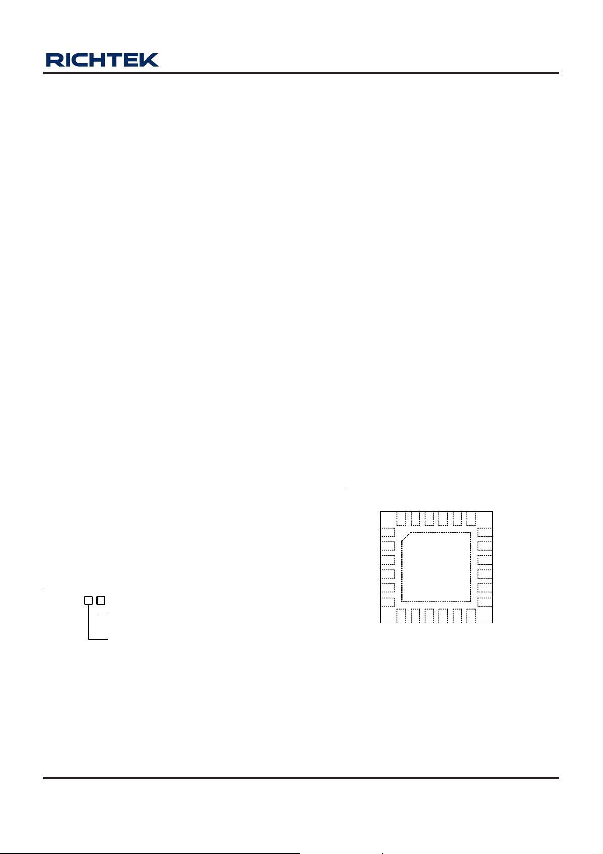
Pin Configurations
(TOP VIEW)
FB5 FB2
11
EN4
25
PVDD5
SEL
LX3
18
17
16
15
14
13
LX2
PVDD2
VDDM
FB3
EN2
PVDD3
LX1
PVDD1
EN3
FB4
SS
PVDD4
EN1
GND
24 2223
1
2
3
4
5
6
7
8910 12
LX4
EN5
WQFN-24L 4x4
FB1
21 20 19
GND
VOUT5
Marking Information
For marking information, contact our sales representative
directly or through a Richtek distributor located in your
area.
DS9953-02 April 2011 www.richtek.com
1
Page 2
RT9953
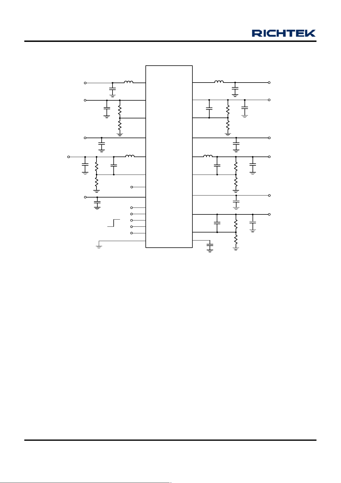
Typical Application Circuit
For 2AA
C10
10µF
C4
10µF
C12
33pF
V
2.2µH
R3
470k
R4
88.7k
4.7µH
BAT
V
OUT_CH4
1.8V
V
OUT_CH2
10µF
V
BAT
C11
3.6V
5V
C5
10µF x 2
R7
470k
R8
374k
C16
1µF
Chip Enable
23, 25 (Exposed Pad)
L2
L4
18
17
21
19
16
24
14
20
6
7
4
VDDM
3
8
LX2
PVDD2
FB2
PVDD43.6V
LX4
FB4
SEL
EN1
EN2
EN3
EN4
EN5
GND
RT9953
1
LX1 V
2
PVDD1
22
FB1
13
PVDD3
12
LX3
15
FB3
11
PVDD5 3.6V
9
VOUT5
10
FB5
5
SS
L3
4.7µH
L1
2.2µH
C3
4.7pF
C9
22pF
C15
10pF
C17
0.47nF
R1
470k
R2
133k
C1
10µF
C7
10µF
R5
768k
R6
360k
C13
1µF
R9
47k
R10
22.1k
C2
10µF x 2
C8
10µF
C14
1µF
BAT
V
OUT_CH1
3.6V
3.6V
V
OUT_CH3
2.5V
V
OUT_CH5
2.5V
DS9953-02 April 2011www.richtek.com
2
Page 3
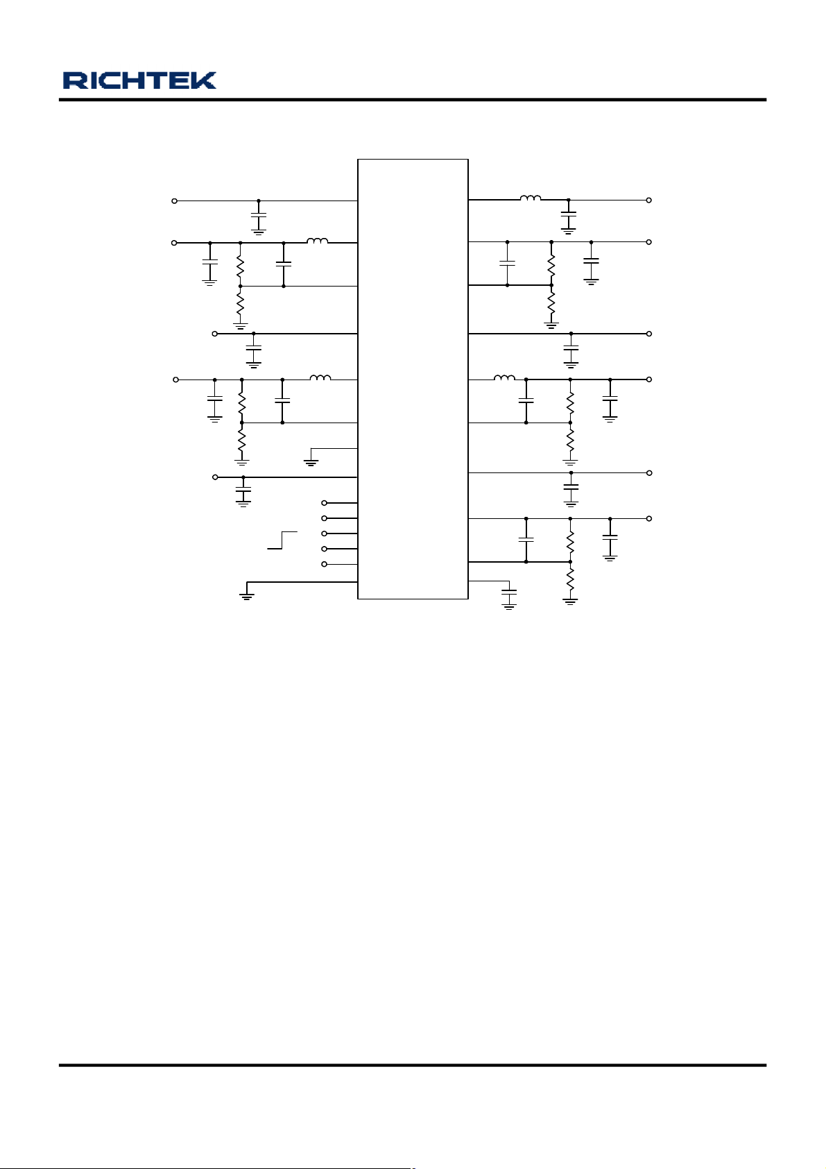
For Li-ion
RT9953
V
OUT_CH2
V
OUT_CH4
V
BAT
or 5V
3.3V
1.8V
C5
10µF
V
C11
10µF
BAT
5V
C4
10µF
L2
2.2µH
R3
470k
R4
150k
R7
470k
R8
374k
C6
10pF
C10
10µF
C16
1µF
Chip Enable
23, 25 (Exposed Pad)
4.7µH
C12
33pF
L4
16
17
18
21
6
7
4
19
24
14
3
20
8
PVDD2
LX2
FB2
PVDD4
LX4
FB4
SEL
VDDM
EN1
EN2
EN3
EN4
EN5
GND
RT9953
L1
L3
4.7µH
2.2µH
C3
4.7pF
C17
0.47nF
C9
22pF
C15
10pF
R1
470k
R2
88.7k
C1
10µF
C7
10µF
R5
768k
R6
360k
C13
1µF
R9
47k
R10
22.1k
C2
10µF x 2
1
LX1 V
2
PVDD1
22
FB1
13
PVDD3
12
LX3
15
FB3
11
PVDD5
9
VOUT5
10
FB5
5
SS
C8
10µF
C14
1µF
BAT
V
OUT_CH1
5V
V
BAT
V
OUT_CH3
2.5V
V
BAT
V
OUT_CH5
2.5V
DS9953-02 April 2011 www.richtek.com
3
Page 4
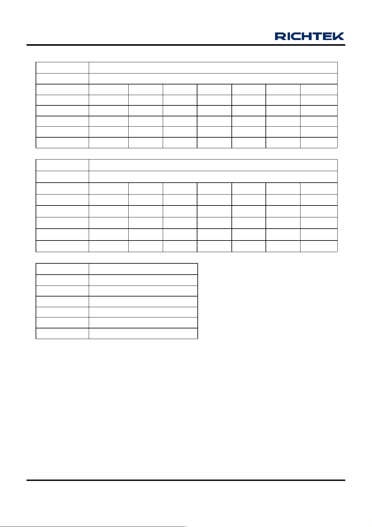
RT9953
Channel CH3
Table 1. Recommended Components for the Typical Application Circuit
Formula V
V
OUT_CH3
L3 (µH) 4.7 4.7 4.7 4.7 4.7 4.7 4.7
R5 (kΩ) 86.6 768 470 330 237 187 23.2
R6 (kΩ) 27.4 360 374 374 374 374 93.1
C9 (pF) 22 22 33 47 68 82 47
C8 (µF) 10 10 10 10 10 10 10
(V) 3.3 2.5 1.8 1.5 1.3 1.2 1.0
OUT_CH3
= (1+R5/R6) x 0.8
Channel CH4
Application
V
OUT_CH4
L4 (µH)
R7 (kΩ) 86.6 768 470 330 237 187 23.2
R8 (kΩ) 27.4 360 374 374 374 374 93.1
C12 (pF) 22 22 33 47 68 82 47
C11 (µF) 10 10 10 10 10 10 10
(V)
3.3 2.5 1.8 1.5 1.3 1.2 1.0
4.7 4.7 4.7 4.7 4.7 4.7 4.7
V
OUT_CH4
= (1+R7/R8) x 0.8
Channel CH5
Formula V
V
OUT_CH5
R9 (kΩ) 47
R10 (kΩ) 22.1
C15 (pF) 10
C14 (µF) 1
(V) 2.5
OUT_CH5
= (1+R9/R10) x 0.8
DS9953-02 April 2011www.richtek.com
4
Page 5
Functional Pin Description
Pin No. Pin Name
1 LX1 Switch Node of CH1. High impedance in shutdown mode.
2 PVDD1 Power Input of CH1.
3 EN3 Enable Control Input of CH3.
4 FB4 Feedback Input of CH4. High impedance in shutdown mode.
5 SS Soft-Start Control Input.
6 PVDD4 Power Input of CH4.
7 LX4 Switch Node of CH7. High impedance in shutdown mode.
8 EN5 Enable Control Input of CH5.
9 VOUT5 Output Voltage of CH5.
10 FB5 Feedback Input of CH5. High impedance in shutdown mode.
11 PVDD5 Power Input of CH5.
12 LX3 Switch Node of CH3. High impedance in shutdown mode.
13 PVDD3 Power Input of CH3.
14 EN2 Enable Control Input of CH2.
15 FB3 Feedback Input of CH3. High impedance in shutdown mode.
16 VDDM Analog Power Input.
17 PVDD2 Power Input of CH2.
RT9953
Pin Function
18 LX2 Switch Node of CH2. High impedance in shutdown mode.
19 SEL
20 EN4 Enable Control Input of CH4.
21 FB2 Feedback Input of CH2. High impedance in shutdown mode.
22 FB1 Feedback Input of CH1. High impedance in shutdown mode.
23,
25 (Exposed Pad)
24 EN1 Enable Control Input of CH1.
GND
Selection Input for CH2 step-up or step-down operation mode. Logic state can
not be changed during operation.
Ground Pin. The exposed pad must be soldered to a large PCB and connected to
GND for maximum thermal dissipation.
DS9953-02 April 2011 www.richtek.com
5
Page 6
RT9953
Function Block Diagram
VDDM
PVDD2
LX2
FB2
PVDD4
LX4
FB4
EN1
EN2
EN3
EN4
EN5
SEL
0.8V
REF
0.8V
REF
CH2
C-Mode
Step-Up or
Step-Down
+
CH4
C-Mode
Step-Down
+
Enable Mode
Sequence
CH1
C-Mode
Step-Up
CH3
C-Mode
Step-Down
VDDM
CH5
LDO
PVDD1
LX1
-
+
0.8V
REF
+
0.8V
REF
+
0.8V
REF
FB1
PVDD3
LX3
FB3
PVDD5
SS
VOUT5
FB5
GND
DS9953-02 April 2011www.richtek.com
6
Page 7

RT9953
Absolute Maximum Ratings (Note 1)
l Supply Voltage, VDDM, PVDD5--------------------------------------------------------------------------------------0.3V to 7V
l Power Switch :
LX1, LX2, LX3, LX4------------------------------------------------------------------------------------------------------- −0.3V to 6.5V
l The Other Pins----------------------------------------------------------------------------------------------------------- −0.3V to 6.5V
l Power Dissipation, P
WQFN 24L 4x4-----------------------------------------------------------------------------------------------------------1.852W
l Package Thermal Resistance (Note 2)
WQFN 24L 4x4, θJA-----------------------------------------------------------------------------------------------------54°C/W
WQFN 24L 4x4, θJC-----------------------------------------------------------------------------------------------------7°C/W
l Junction Temperature---------------------------------------------------------------------------------------------------150°C
l Lead Temperature (Soldering, 10 sec.)------------------------------------------------------------------------------260°C
l Storage Temperature Range------------------------------------------------------------------------------------------- −65°C to 150°C
l ESD Susceptibility (Note 3)
HBM (Human Body Mode)---------------------------------------------------------------------------------------------2kV
MM (Machine Mode)----------------------------------------------------------------------------------------------------200V
Recommended Operating Conditions (Note 4)
@ T
D
= 25°C
A
l Junction Temperature Range------------------------------------------------------------------------------------------ −40°C to 125°C
l Ambient Temperature Range------------------------------------------------------------------------------------------ −40°C to 85°C
Electrical Characteristics
(V
= 3.3V, T
DDM
Supply Voltage
VDDM Operating Voltage V
VDDM Startup Voltage VST 1.5 -- -- V
VDDM Over Voltage Protection 5.7 6 6.25
PVDD5 Operating Voltage V
Supply Current
Shutdown Supply Current into VDDM I
CH1 (Syn Step-Up) : Supply Current
into VDDM
CH2 (Syn Step-Up or Syn
Step-Down) : Supply Current into
VDDM
CH3 (Syn Step-Down) :
Supply Current into VDDM
CH4 (Syn Step-Down) :
Supply Current into VDDM
CH5 (LDO) :
Supply Current into PVDD5
= 25°C, unless otherwise specified)
A
Parameter Symbol
2.7 -- 5.5 V
DDM
PVDD5
All EN = 0 -- -- 0.1 µA
OFF
IQ1 Non Switching, EN1 = 3.3V -- -- 800 µA
IQ2 Non Switching, EN2 = 3.3V -- -- 800 µA
IQ3 Non Switching, EN3 = 3.3V -- -- 800 µA
IQ4 Non Switching, EN4 = 3.3V -- -- 800 µA
IQ5 EN5 = 3.3V, I
Test Conditions Min Typ Max Unit
V
2.5 -- 5.5 V
= 0mA -- 90 130 µA
OUT
To be continued
DS9953-02 April 2011 www.richtek.com
7
Page 8

RT9953
Parameter Symbol
Test Conditions Min Typ Max Unit
Oscillator
CH1,2,3,4 Operating Frequency f
CH1 Maximum Duty Cycle (Step-Up) V
CH2 Maximum Duty Cycle (Step-Up) V
CH2 Maximum Duty Cycle
(Step-Down)
CH3 Maximum Duty Cycle
(Step-Down)
CH4 Maximum Duty Cycle
(Step-Down)
900 1000 1100 kHz
OSC
= 0.7V 80 83 86 %
FB1
= 0.7V 80 83 86 %
FB2
V
V
V
= 0.7V -- -- 100 %
FB2
= 0.7V -- -- 100 %
FB3
= 0.7V -- -- 100 %
FB4
Feedback Regulation Voltage
Feedback Regulation Voltage @ FB1,
FB2, FB3, FB4, FB5
Total Accuracy (Including load
regulation and line regulation)
0.788 0.8 0.812 V
−3 -- 3 %
Power Switch
CH1 On Resistance of MOSFET R
DS(ON)
P-MOSFET, PVDD1 = 3.3V -- 200 250
N-MOSFET, PVDD1 = 3.3V -- 150 200
mΩ
CH1 Current Limitation (Step-Up) -- 3 -- A
CH2 On Resistance of MOSFET R
DS(ON)
P-MOSFET, PVDD2 = 3.3V -- 200 250
N-MOSFET, PVDD2 = 3.3V -- 150 200
mΩ
CH2 Current Limitation (Step-Down) -- 1.8 -- A
CH2 Current Limitation (Step-Up) -- 3 -- A
CH3 On Resistance of MOSFET
R
DS(ON)
P-MOSFET, PVDD3 = 3.3V -- 350 400
N-MOSFET, PVDD3 = 3.3V -- 300 400
mΩ
CH3 Current Limitation (Step-Down) -- 1.5 -- A
CH4 On Resistance of MOSFET
R
DS(ON)
P-MOSFET, PVDD4 = 3.3V -- 350 400
N-MOSFET, PVDD4 = 3.3V -- 300 400
mΩ
CH4 Current Limitation (Step-Down) -- 1.5 -- A
CH5 Dropout Voltage (LDO) V
Drop
2.2V ≦ PVDD5 ≦ 2.7V,
I
= 400mA
OUT
2.7V ≦ PVDD5 ≦ 5.5V,
I
= 500mA
OUT
-- 160 320
mV
-- 250 400
Protection
Over Voltage Protection of CH1, CH2
Step-Up, PVDD1 and PVDD2
5.7 6 6.25 V
Over Voltage Protection Hysteresis of
CH1, CH2 Step-Up, PVDD1 and
-- 0.5 -- V
PVDD2
Under Voltage Protection (CH1 to
CH5)
FB Threshold 0.36 0.4 0.44
2.2V ≦ PVDD5 ≦ 2.7V 0.4 0.7 1.05
CH5 Current Limit I
LIM
2.7V ≦ PVDD5 ≦ 5.5V 0.5 0.8 1.05
Protection Fault Delay -- 100 -- ms
8
To be continued
DS9953-02 April 2011www.richtek.com
V
A
Page 9

RT9953
Parameter Symbol
Test Conditions Min
Typ Max Unit
Control
Logic High 1.3 -- 5.5 V EN1 to EN5, SEL
Input Threshold
Logic Low -- -- 0.4 V
EN1 to EN5, SEL Sink Current -- 2 6 µA
CH5 LDO Regulation
Line Regulation ΔV
Load Regulation ΔV
Rejection Rate
f = 100Hz -- −60 -- Power Supply
f = 10kHz
PSRR C
LINE
LOAD
V
I
OUT
1mA < I
PVDD5
= 1mA
= 1uF, I
OUT
= (V
OUT
+ 1V) to 5.5V
OUT5
-- -- 0.3 %
< 300mA -- -- 0.6 %
= 100mA
OUT
-- −30 --
dB
Thermal Protection
Thermal Shutdown TSD 125
160 -- °C
Thermal Shutdown Hysteresis ΔTSD -- 20 -- °C
Note 1. Stresses listed as the above “ Absolute Maximum Ratings” may cause permanent damage to the device. These
are for stress ratings. Functional operation of the device at these or any other conditions beyond those indicated
in the operational sections of the specifications is not implied. Exposure to absolute maximum rating conditions
for extended periods may remain possibility to affect device reliability.
Note 2. θJA is measured in the natural convection at T
= 25°C on a high effective four layers thermal conductivity test
A
board of JEDEC 51-7 thermal measurement standard. The case point of θJC is on the expose pad for the WQFN
package.
Note 3. Devices are ESD sensitive. Handling precaution is recommended.
Note 4. The device is not guaranteed to function outside its operating conditions.
DS9953-02 April 2011 www.richtek.com
9
Page 10

RT9953
Typical Operating Characteristics
CH1 Step-Up Efficiency vs. Output Current
100
90
80
70
60
50
V
V
V
V
V
V
BAT
BAT
BAT
BAT
BAT
BAT
= 4.5V
= 4.2V
= 3.9V
= 3.6V
= 3.3V
= 3V
40
Efficiency (%)
30
20
10
= 5V, V
DDM
L1 = 2.2µH, C2 = 10µFx2
OUT_CH1
= 5V,
V
0
10 100 1000
Output Current (mA)
CH2 Step-Down Efficiency vs. Output Current
100
90
80
70
60
50
40
Efficiency (%)
30
20
10
0
10 100 1000
V
= 1.8V
BAT
V
= 3V
BAT
V
= 3.3V
BAT
V
= 3.6V
BAT
V
= 4.2V
BAT
V
= 4.5V
BAT
V
L2 = 4.7µH, C5 = 10µF
Output Current (mA)
DDM
= 5V, V
OUT_CH2
= 1.2V,
CH1 Step-Up Efficiency vs. Output Current
100
90
80
70
60
50
V
V
V
V
V
V
BAT
BAT
BAT
BAT
BAT
BAT
= 3.4V
= 3V
= 2.7V
= 2.5V
= 2.2V
= 1.8V
40
Efficiency (%)
30
20
10
DDM
L1 = 2.2µH, C2 = 10µFx2
OUT_CH1
V
= 3V, V
0
10 100 1000
Output Current (mA)
CH2 Step-Up Efficiency vs. Output Current
100
90
80
70
60
50
40
Efficiency (%)
30
20
10
0
10 100 1000
Output Current (mA)
V
= 3V
BAT
V
= 2.7V
BAT
V
= 2.5V
BAT
V
= 2.2V
BAT
V
= 2V
BAT
V
= 1.8V
BAT
V
DDM
= 3V, V
OUT_CH2
= 3.3V,
L2 = 2.2µH, C5 = 10µFx2
= 5V,
CH3 Step-Down Efficiency vs. Output Current
100
90
80
10
70
60
50
40
Efficiency (%)
30
20
10
0
10 100 1000
V
= 2.7V
BAT
V
= 3.3V
BAT
V
= 3.6V
BAT
V
= 3.9V
BAT
V
= 4.2V
BAT
V
= 4.5V
BAT
Output Current (mA)
V
= 5V, V
DDM
OUT_CH3
L3 = 4.7µH, C8 = 10µF
= 1.8V,
CH3 Step-Down Efficiency vs. Output Current
100
90
80
Efficiency (%)
70
60
50
40
30
20
10
V
= 1.8V
BAT
V
= 2.5V
BAT
V
= 3V
BAT
V
= 3.3V
BAT
V
= 3.6V
BAT
V
= 4.5V
BAT
V
DDM
= 5V, V
OUT_CH3
= 1.2V,
L3 = 4.7µH, C8 = 10µF
0
10 100 1000
Output Current (mA)
DS9953-02 April 2011www.richtek.com
Page 11

RT9953
CH4 Step-Down Efficiency vs. Output Current
100
90
V
= 3.4V
BAT
V
= 3.6V
BAT
V
= 3.9V
BAT
V
= 4.2V
BAT
V
= 4.5V
BAT
V
DDM
= 5V, V
OUT_CH4
= 3.3V,
L4 = 4.7µH, C11 = 10µF
10 100 1000
Efficiency (%)
80
70
60
50
40
30
20
10
0
Output Current (mA)
CH1 Step-Up Output Voltage vs. Output Current
5.000
4.995
4.990
Output Voltage (V)
4.985
4.980
4.975
4.970
4.965
4.960
4.955
4.950
0 100 200 300 400 500 600
Output Current (mA)
V
V
V
BAT
DDM
= 3V
BAT
= 4.5V
= 5V
CH4 Step-Down Efficiency vs. Output Current
100
90
80
70
V
= 1.8V
60
50
40
Efficiency (%)
30
20
10
0
10 100 1000
V
V
V
V
V
BAT
BAT
BAT
BAT
BAT
BAT
= 2.5V
= 3V
= 3.3V
= 3.6V
= 4.5V
V
DDM
= 3V, V
OUT_CH4
= 1.2V,
L4 = 4.7µH, C11 = 10µF
Output Current (mA)
CH2 Step-Down Output Voltage vs. Output Current
1.210
1.208
1.205
1.203
Output Voltage (V)
1.200
1.198
1.195
1.193
1.190
0 200 400 600 800 1000
Output Current (mA)
V
V
V
BAT
BAT
DDM
= 3V
= 4.5V
= 5V
CH2 Step-Up Output Voltage vs. Output Current
3.45
3.40
3.35
CH3 Step-Down Output Voltage vs. Output Current
1.85
1.84
1.83
1.82
3.30
3.25
Output Voltage (V)
3.20
3.15
0 100 200 300 400 500 600
Output Current (mA)
V
V
V
BAT
BAT
DDM
= 1.8V
= 3V
= 3V
1.81
1.80
Output Voltage (V)
1.79
1.78
0 100 200 300 400 500 600
Output Current (mA)
V
V
V
BAT
BAT
BAT
V
DDM
= 4.5V
= 3V
= 2.7V
= 5V
DS9953-02 April 2011 www.richtek.com
11
Page 12

RT9953
CH4 Step-Down Output Voltage vs . Output Current
3.50
3.45
3.40
3.35
V
= 4.5V
BAT
V
= 5V
3.30
3.25
Output Voltage (V)
3.20
3.15
0 100 200 300 400 500 600
BAT
V
DDM
= 5V
Output Current (mA)
CH2 Step-Down Output Voltage Ripple
LX2
(2V/Div)
LX1
(2V/Div)
V
OUT_CH1_ac
(10mV/Div)
LX2
(2V/Div)
CH1 Output Voltage Ripple
V
= 5V, V
DDM
I
= 300mA, L1 = 2.2μH, C2 = 10μFx2
OUT
= 3.7V, V
BAT
OUT_CH1
= 5V,
Time (500ns/Div)
CH2 Step-Up Output Voltage Ripple
V
OUT_CH2_ac
(5mV/Div)
LX3
(2V/Div)
V
OUT_CH3_ac
(5mV/Div)
V
= 5V, V
DDM
= 300mA, L2 = 2.2μH, C5 = 10μF
I
OUT
= 3.7V, V
BAT
OUT_CH2
Time (500ns/Div)
CH3 Output Voltage Ripple
V
= 5V, V
DDM
I
= 300mA, L3 = 4.7μH, C8 = 10μF
OUT
= 3.7V, V
BAT
OUT_CH3
= 1.2V,
= 1.8V,
V
OUT_CH2_ac
(10mV/Div)
LX4
(2V/Div)
V
OUT_CH4_ac
(5mV/Div)
V
= 3V, V
DDM
= 300mA, L2 = 2.2μH, C5 = 10μFx2
I
OUT
= 1.8V, V
BAT
OUT_CH2
Time (500ns/Div)
CH4 Output Voltage Ripple
V
= 5V, V
DDM
I
= 300mA, L4 = 4.7μH, C11 = 10μF
OUT
= 4.2V, V
BAT
OUT_CH4
= 3.3V,
= 3.3V,
12
Time (500ns/Div)
Time (500ns/Div)
DS9953-02 April 2011www.richtek.com
Page 13

RT9953
)
I
LOAD
(200mA/Div)
V
OUT_CH1_ac
(100mV/Div)
I
LOAD
(200mA/Div)
CH1 Load Transient Response
V
= 5V, V
DDM
= 100mA to 400mA, L1 = 2.2μH, C2 = 10μFx2
I
OUT
BAT
= 3V, V
OUT_CH1
= 5V,
Time (1ms/Div)
CH2 Step-Up Load Transient Response
CH2 Step-Down Load Transient Response
I
LOAD
(200mA/Div)
V
OUT_CH2_ac
(50mV/Div)
I
LOAD
(200mA/Div)
V
= 5V, V
DDM
= 100mA to 400mA, L2 = 2.2μH, C5 = 10μF
I
OUT
= 3.7V, V
BAT
OUT_CH2
= 1.2V,
Time (1ms/Div)
CH3 Load Transient Response
V
OUT_CH2_ac
(100mV/Div)
I
LOAD
(200mA/Div)
V
OUT_CH4_ac
(50mV/Div)
V
= 3V, V
DDM
= 100mA to 400mA, L2 = 2.2μH, C5 = 10μFx2
I
OUT
= 1.8V, V
BAT
OUT_CH2
= 3.3V,
Time (1ms/Div)
CH4 Load Transient Response
V
= 5V, V
DDM
I
= 50mA to 300mA, L4 = 4.7μH, C11 = 10μF
OUT
= 3.7V, V
BAT
OUT_CH4
Time (1ms/Div)
= 3.3V,
V
OUT_CH3_ac
(50mV/Div)
1050
1030
1010
Frequency (kHz
V
= 5V, V
DDM
I
= 50mA to 300mA, L3 = 4.7μH, C8 = 10μF
OUT
= 3.7V, V
BAT
OUT_CH3
= 1.8V,
Time (1ms/Div)
Frequency vs. Temperature
990
970
950
930
910
890
870
850
-40-30-20-100 102030405060708090
Temperature (°C)
V
DDM
= 3V, V
BAT
= 3V
DS9953-02 April 2011 www.richtek.com
13
Page 14

RT9953
)
CH5 LDO Output Voltage vs. Output Current
2.55
2.54
2.53
2.52
2.51
2.50
2.49
2.48
Output Voltage (V)
2.47
2.46
2.45
I
LOAD
(200mA/Div)
V
OUT_CH5_ac
(10mV/Div)
V
= 3V
BAT
= 4.5V
V
BAT
V
= 5V
DDM
0 100 200 300 400 500 600
Output Current (mA)
CH5 LDO Load Transient Response
V
= 5V, V
DDM
= 1mA to 300mA, C14 = 1μF
I
OUT
= 3.7V, V
BAT
Time (1ms/Div)
OUT_CH5
= 2.5V,
CH5 LDO Dropout Voltage vs. Output Current
0.45
0.40
0.35
0.30
0.25
0.20
0.15
Dropout Voltage (V)
0.10
0.05
0.00
0 100 200 300 400 500
V
DDM
90°C
25°C
= 5V, C14 = 1μF
Output Current (mA)
CH5 LDO Output Voltage v s. Te m perature
2.55
2.54
2.53
2.52
2.51
V
= 4.5V
2.50
2.49
2.48
Output Voltage (V)
2.47
2.46
2.45
BAT
V
= 3V
BAT
V
= 5V, C14 = 1μF, I
DDM
-40-30-20-100 102030405060708090
= 300mA
OUT
Temperature (°C)
−40°C
0
CH5 LDO PSRR
-10
-20
-30
-40
-50
PSRR (dB)
V
= 5V
BAT
= 3.7V
V
-60
-70
-80
BAT
V
= 5V, C14 = 1μF, I
DDM
10 100 1000 10000 100000 1000000
= 100mA
OUT
Frequency (Hz)
CH5 LDO I
130
120
110
100
90
80
70
60
Quiescent Current (μA
50
40
30
-40-30-20-10 0 102030405060708090
Quiescent Current vs. Temperature
PVDD5
V
DDM
= 3.3V, V
= 3.3V, C14 = 1μF, I
BAT
Temperature (°C)
OUT
= 0mA
DS9953-02 April 2011www.richtek.com
14
Page 15
Application information
RT9953
The RT9953 includes the following four DC/DC converters
and one LDO to build a multiple-output power-supply
system.
CH1 : Synchronous Step-Up DC/DC Converter
The CH1 is a synchronous step-up converter for motor or
DSC system I/O power. The converter operates at fixed
frequency and PWM Current Mode. The CH1 converter
integrated internal MOSFETs, compensation network and
synchronous rectifier for up to 95% efficiency.
The output voltage can be set by the following equation :
V
OUT_CH1
Where V
= (1+R1/R2) x V
FB1
is 0.8V typically.
FB1
CH2 : Synchronous Step-Up or Step-Down
Selectable DC/DC Converter
The CH2 is a synchronous step-up/step-down selectable
converter for motor or DSC system I/O power.
Mode setting
The CH2 of RT9953 features flexible Step-up or Step-down
topology setting for either 1 x Li-ion or 2 x AA application
by SEL pin. Please refer to “Electrical Characteristics”
for level of Logic-High or Logic-Low. When the CH2
operates as a Step-up converter, the SEL must be set at
Logic-High. If the CH2 operates at Step-down mode, the
SEL must be set at Logic-Low. In addition, please note
that the logic state can not be changed during operation.
Step-Down :
The converter operates at fixed frequency PWM mode
and continuous current mode (CCM) with internal
MOSFETs, compensation network and synchronous
rectifier for up to 95% efficiency. The CH2 Step-down
converter can be operating at 100% maximum duty cycle
to extend the input operating voltage range. While the
input voltage is close to the output voltage, the converter
enters low dropout mode.
The output voltage can be set by the following equation :
V
OUT_CH2
Where V
= (1+R3/R4) x V
is 0.8V typically.
FB2
FB2
CH3 and CH4 : Synchronous Step-Down DC/DC
Converter
The converter operates at fixed frequency PWM mode,
CCM and integrated internal MOSFETs and compensation
network. The CH3 and CH4 Step-down converter can be
operating at 100% maximum duty cycle to extend battery
operating voltage range. When the input voltage is close
to the output voltage, the converter could enter low dropout
mode with low output ripple.
The output voltage can be set by the following equation :
V
OUT_CH3
V
OUT_CH4
Where V
= (1+R5/R6) x V
= (1+R7/R8) x V
FB3
and V
is 0.8V typically.
FB4
FB3
FB4
Table 2. CH2 Mode Setting
SEL CH2 Operating Mode
Logic-High Step-Up
CH5 : 500mA Low Dropout, Low Noise Linear
Regulator
Like any low-dropout regulator, this CH requires input and
output decoupling capacitors. The CH5 linear regulator
Logic-Low Step-Down
can support 500mA output current when PVDD5 > 2.7V.
The typical current limit is 0.8A. If the output is shorted to
Step-Up :
The converter operates at fixed frequency PWM Mode,
continuous current mode (CCM), and discontinuous current
mode (DCM) with internal MOSFETs, compensation
network and synchronous rectifier for up to 95% efficiency.
DS9953-02 April 2011 www.richtek.com
ground, the Under Voltage Protection function will be
triggered to shutdown the IC to prevent the part from
damaging.
The output voltage can be set by the following equation :
V
OUT_CH5
Where V
= (1+R9/R10) x V
is 0.8V typically.
FB5
FB5
15
Page 16

RT9953
Thermal Considerations
For continuous operation, do not exceed absolute
maximum operation junction temperature. The maximum
power dissipation depends on the thermal resistance of
IC package, PCB layout, the rate of surroundings airflow
and temperature difference between junction to ambient.
The maximum power dissipation can be calculated by
following formula :
P
Where T
temperature, T
D(MAX)
= (T
J(MAX)
− TA ) / θ
J(MAX)
JA
is the maximum operation junction
is the ambient temperature and the θ
A
JA
the junction to ambient thermal resistance.
For recommended operating conditions specification of
RT9953, the maximum junction temperature is 125°C. The
junction to ambient thermal resistance θJA is layout
dependent. For WQFN-24L 4x4 package, the thermal
resistance θJA is 54°C/W on the standard JEDEC 51-7
four layers thermal test board. The maximum power
dissipation at TA = 25°C can be calculated by following
formula :
Layout Considerations
For the best performance of the RT9953, the following
PCB layout guidelines must be strictly followed :
} Place the input and output capacitors as close as
possible to the input and output pins respectively for
good filtering.
} Keep the main power traces as wide and short as
possible.
} The switching node area connected to LX and inductor
should be minimized for lower EMI.
is
} Place the feedback components as close as possible
to the FB pin and keep these components away from
the noisy devices.
} Connect the GND and Exposed Pad to a strong ground
plane for maximum thermal dissipation and noise
protection.
} CH5 PCB trace and component had put different PCB
side to avoid LX3 and LX4 switching noise.
P
= (125°C − 25°C) / (54°C/W) = 1.852W for
D(MAX)
WQFN-24L 4x4
The maximum power dissipation depends on operating
ambient temperature for fixed T
and thermal
J(MAX)
resistance θJA. For RT9953 package, the Figure 1 of
derating curve allows the designer to see the effect of
rising ambient temperature on the maximum power
dissipation allowed.
2.0
1.8
1.6
1.4
1.2
1.0
0.8
0.6
0.4
0.2
Maximum Power Dissipation (W)
0.0
0 25 50 75 100 125
WQFN-24L 4x4
Ambient Temperature (°C)
Four Layers PCB
Figure 1. Derating Curves for RT9953 Package
16
DS9953-02 April 2011www.richtek.com
Page 17

RT9953
LX should be connected to Inductor by
wide and short trace, keep sensitive
compontents away from this trace
Input/Output
capacitors must
be placed as
close as possible
to the Input/
Output pins.
V
BAT
GND
V
OUT1_CH1
R7 R8
C12
V
BAT
GND
V
OUT4_CH4
GND
C2
C17
L1
PVDD1
EN3
PVDD4
C10
C11
C1
LX1
FB4
SS
L4
1
2
3
4
5
6
GND
EN1
24 2223
7
LX4
OUT5_CH5
V
C14
Place the feedback components as
close as possible to the FB pin and
keep away from noisy devices.
C6
R1
C3
R3
R2
FB2
GND
FB1
EN4
21 20 19
GND
25
8 9 10 12
EN5
R9
VOUT5
C15
FB5
R10
11
PVDD5
BAT
V
C13
OUT2_CH2
R4
SEL
18
LX2
17
PVDD2
16
VDDM
15
FB3
14
EN2
13
PVDD3
LX3
L3
Connect the Exposed
Pad to a ground plane.
L2
R6
C5
C7
C8
V
GNDV
C4
V
BAT
C16
V
BAT
GND
OUT3_CH3
R5
C9
Figure 2. PCB Layout Guide
DS9953-02 April 2011 www.richtek.com
17
Page 18

RT9953
V
Current Limit
PVDD1 OVP
Current Limit
PVDD2 OVP
Current Limit
V
DDM
CH1
Step-Up
CH2
Step-Up
CH2
Step-Down
CH3
Step-Down
CH4
Step-Down
CH5 LDO
Thermal
Over Voltage
Protection
OCP P-MOSFET current > 1.5A IC shutdown 100ms V
UVP FB2 < 0.4V IC shutdown 100ms V
OCP P-MOSFET current > 1.5A IC shutdown 100ms V
UVP FB3 < 0.4V IC shutdown 100ms V
OCP P-MOSFET current > 1.5A IC shutdown 100ms V
UVP FB4 < 0.4V IC shutdown 100ms V
UVP FB5 < 0.4V IC shutdown 100ms V
Thermal
shutdown
Protection
type
Table 3. Protection Items
Threshold (typical)
Refer to Electrical spec
V
> 6V Disable all channels 100ms
DDM
Protection methods
Delay
time
N-MOSFET current > 3A IC shutdown 100ms V
PVDD1 > 6V IC shutdown No-delay V
N-MOSFET current > 3A IC shutdown 100ms V
PVDD2 > 6V IC shutdown No-delay V
I
(P-MOSFET current) >
OUT
0.8A
Temperature > 160°C
Current Limiting No-delay No reset
All channels stop
switching
100ms Temperature < 140°C
Reset method
Restart if V
DDM
(with hysteresis)
power reset
DDM
power reset
DDM
power reset
DDM
power reset
DDM
power reset
DDM
power reset
DDM
power reset
DDM
power reset
DDM
power reset
DDM
power reset
DDM
power reset
DDM
< 5.5
18
DS9953-02 April 2011www.richtek.com
Page 19

Outline Dimension
RT9953
D
E
A
A3
A1
D2
SEE DETAIL A
L
1
E2
1
2
be
Pin #1 ID and Tie Bar Mark Options
DETAIL A
Note : The configuration of the Pin #1 identifier is optional,
1
2
but must be located within the zone indicated.
Dimensions In Millimeters
Dimensions In Inches
Symbol
Min Max Min Max
A 0.700 0.800 0.028 0.031
A1 0.000 0.050 0.000 0.002
A3 0.175 0.250 0.007 0.010
b 0.180 0.300 0.007 0.012
D 3.950 4.050 0.156 0.159
D2 2.300 2.750 0.091 0.108
E 3.950 4.050 0.156 0.159
E2 2.300 2.750 0.091 0.108
e 0.500 0.020
L 0.350 0.450
Richtek Technology Corporation
Headquarter
5F, No. 20, Taiyuen Street, Chupei City
Hsinchu, Taiwan, R.O.C.
Tel: (8863)5526789 Fax: (8863)5526611
0.014 0.018
W-Type 24L QFN 4x4 Package
Richtek Technology Corporation
Taipei Office (Marketing)
5F, No. 95, Minchiuan Road, Hsintien City
Taipei County, Taiwan, R.O.C.
Tel: (8862)86672399 Fax: (8862)86672377
Email: marketing@richtek.com
Information that is provided by Richtek Technology Corporation is believed to be accurate and reliable. Richtek reserves the right to make any change in circuit
design, specification or other related things if necessary without notice at any time. No third party intellectual property infringement of the applications should be
guaranteed by users when integrating Richtek products into any application. No legal responsibility for any said applications is assumed by Richtek.
DS9953-02 April 2011 www.richtek.com
19
Page 20

 Loading...