

Page 1
RT9912A
Multi-Channel Power Management IC for Portable Device
General Description
The RT9912A is a multi-channel power management IC
providing power conversion and system power ma nagement functions for one or two alkaline battery powered
portable handheld device.
The RT9912A integrates one high efficiency synchronous
buck regulator, one high efficiency boost regulator, one
linear regulator and one adjustable voltage detector for
reset function.
Ordering Information
RT9912A
Package Type
QW : WQFN-24L 4x4 (W-Type)
Lead Plating System
G : Green (Halogen Free and Pb Free)
Note :
Richtek products are :
` RoHS compliant and compatible with the current require-
ments of IPC/JEDEC J-STD-020.
` Suitable for use in SnPb or Pb-free soldering processes.
Marking Information
For marking information, contact our sales re presentative
directly or through a Richtek distributor located in your
area.
Features
zz
300mA Sync. Step Down Converter for V
z
zz
zz
z 300mA Sync. Step Up Converter for IO and Memory
zz
zz
z High Efficiency Up to 92%
zz
zz
z Low Dropout Linear Regulator
zz
zz
z Adjustable Voltage Detector for Reset Function
zz
zz
z Current Limit Protection
zz
zz
z Thermal Shutdown Protection
zz
zz
z Low Operation Current Consumption
zz
zz
z Small 24-Lead WQFN Package
zz
zz
z RoHS Compliant and Halogen Free
zz
CORE
Applications
z DSC
z Portable Multimedia Player
z GPS
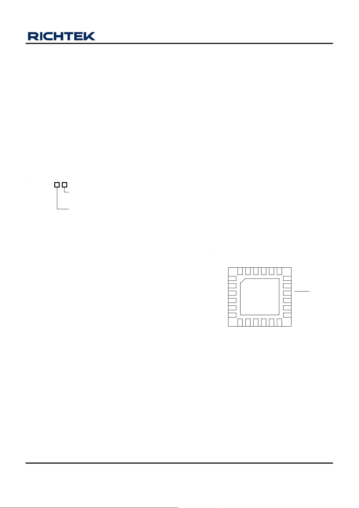
Pin Configurations
(TOP VIEW)
GND
CT
18
FB4
17
VDD4
16
RESET
15
ENBUK
14
25
11
VDD3
13
FB3
VDD1
FB1
ENSW
PSW
NC
ENBST
VOUT1
24 2223
1
2
3
4
5
6
7
LX1
VBAT
21 20 19
GND
8 9 10 12
LX2
FB2
PGND2
PVDD2 PGND1
VDD2
VOUT3
WQFN-24L 4x4
DS9912A-01 April 2011 www.richtek.com
1
Page 2
RT9912A
Typical Application Circuit
V
BAT
VDD3
VDD3V3_IO
C1
1uF
22
14
C3
1uF
17
C2
V
C4
1nF
OUT2
1uF
R4
120k
18
20
16
15
R3
1M
19, Exposed Pad (25)
1
3
6
VDD1
VBAT
VDD3
VDD4
FB4
CT
GND
RESET
ENSW
ENBUK
ENBST
RT9912A
VOUT1
LX1
FB1
PSW
VOUT3
FB3
PGND1
PGND2
PVDD2
VDD2
LX2
FB2
24
23
2
4
12
13
21
8
10
11
9
7
L1
D1
L2 4.7uH
4.7uH
10uF
R5
590k
R6
390k
R7
1.6M
R8
330k
C5
120k
C8
1nF
C12
1uF
C10
100pF
R1
1.2M
R2
C6
2.2pF
C9
4.7uF
C11
10uF
C13
22nF
V
OUT3
3V
VDD2
V
OUT2
1.8V
C7
22uF
Q1
C16
22uF
V
OUT1
3.3V
VDD3V3_IO
Power ON Sequence : V
VDD3V3_IO
→
VDD3V3_IO V
OUT2
ENBUK
ENBST
V
OUT2
PSW
V
OUT3
→
OUT3
DS9912A-01 April 2011www.richtek.com
2
Page 3
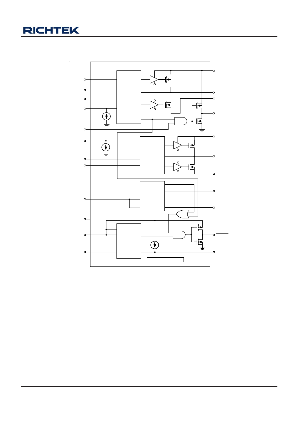
Function Block Diagram
RT9912A
VDD1
VBAT
FB1
ENBST
ENSW
ENBUK
FB2
VDD2
VDD3
VDD1
CH1
Syn-Boost
PFM
CH1
Power
Ready
VDD3
PVDD1
PGND1
PVDD1
PGND1
CH2
Syn-Buck
PFM
CH3
LDO
Regulator
ENLDO
LDOOK
FB3
PVDD2
PGND2
PVDD2
PGND2
VOUT1
LX1
PGND1
PSW
PVDD2
LX2
PGND2
VOUT3
FB3
GND
VDD4
FB4
VDD4
CH4
Reset
Reset
Signal
Delay
RESET
CT
Thermal Protection
DS9912A-01 April 2011 www.richtek.com
3
Page 4

RT9912A
Functional Pin Description
Pin No. Pin Na me Pi n Fun cti o n
1 VDD1 CH1 Power Input Pin.
2 FB1 CH1 Feedback Input Pin.
3 ENSW Load Disconnect Enable Pin.
4 PSW Load Disconnect P-MOSFET Gate Drive Pin.
5 NC No Internal Connection. This pin must be floating.
6 ENBST Boost Enable Pin.
7 FB2 CH2 Feedback Input.
8 PGND2 Power Ground for CH2.
9 LX2 CH2 Switch Node.
10 PVDD2 CH2 Power Input Pin.
11 VDD2 CH2 Power Input Pin for Analog.
12 VOUT3 CH3 Output Voltage.
13 FB3 CH3 Feedback Input.
14 VDD3 CH3 Power Input Pin.
15 ENBUK BUCK Enable Pin.
16 RESET Reset Pulse Output, N egative Pulse.
17 VDD4 CH4 Power Input Pin.
18 FB4 CH4 Feedback Input.
19,
Exposed Pad (25)
20 CT
21 PGND1 Power Ground for CH1.
22 VBAT
23 LX1 CH1 Switch Node.
24 VOUT1 CH1 Output Voltage.
GND
Analog Ground. The exposed pad must be soldered to a large PCB and
connected to GND for maximum power dissipation.
External Delay Adjust Pin.
Battery Power Input Pin.
DS9912A-01 April 2011www.richtek.com
4
Page 5
Absolute Maximum Ratings (Note 1)
T
RT9912A
z Supply Voltage, V
z LX1 and LX2 Pin Switch V oltage ---------------------------------------------------------------------------------------- −0.3V to 6.5V
z Other I/O Pin Voltage------------------------------------------------------------------------------------------------------ −0.3V to 6.5V
z Power Dissipation, P
, V
DD1
DD2
@ TA = 25°C
D
, V
DD3
, V
DD4
, PV
-------------------------------------------------------------------- −0.3V to 6.5V
DD2
WQFN-24L 4x4 ------------------------------------------------------------------------------------------------------------- 1.852W
z Package Thermal Resistance (Note 2)
WQF N-24L 4x4, θJA-------------------------------------------------------------------------------------------------------- 54°C/W
WQFN-24L 4x4, θJC------------------------------------------------------------------------------------------------------- 7°C/W
z Junction T emperature------------------------------------------------------------------------------------------------------ 150°C
z Lead T e mperature (Soldering, 10 sec.)-------------------------------------------------------------------------------- 260 °C
z Storage T emperature Range --------------------------------------------------------------------------------------------- −65°C to 150°C
z ESD Susceptibility (Note 3)
HBM (Human Body Mode) ----------------------------------------------------------------------------------------------- 2kV
MM (Ma chine Mode)------------------------------------------------------------------------------------------------------- 200V
Recommended Operating Conditions (Note 4)
z Supply Input Voltage, V
z Junction T emperature Range---------------------------------------------------------------------------------------------
z Ambient T emperature Range---------------------------------------------------------------------------------------------
----------------------------------------------------------------------------------------------- 1.7V to 5V
BAT
−40°C to 125°C
−40°C to 85°C
Electrical Characteristics
(V
= V
= V
DD1
DD2
DD3
= V
Parameter Symbol Test Condition Min Typ Max Units
Supply Voltage
Minimum Operating Input Voltage RL = 3kΩ -- -- 1.7 V
Minimum Startup Voltage (Boost) V
VDD1 Operating Voltage V
VDD2 Operating Voltage V
VDD3 Operating Voltage V
VDD4 Operating Voltage V
VDD1 Over Voltage Protection 5.1 6 6.5 V
Supply Current
Shutdown Supply Current I
Boost Supply Current I
Buck Supply Current I
DD4
= 3.3V, T
= 25°C, unless otherwise specified)
A
RL = 3kΩ -- 0.8 1.1 V
S
1.7 -- 5 V
DD1
VDD2, PVDD2 Pin Voltage 1.7 -- 5 V
DD2
2.5 -- 5 V
DD3
1.5 -- 5 V
DD4
OFF
VDD1
V
V
V
V
V
V
ENBST
= 0V = V
DD4
= 3.3V, V
DD1
ENBST
OUT1
= V
DD2
= V
ENSW
= V
ENSW
= 3.3V
DD3
DD3
FB1
= V
= 0V
= 0.9V
= 3.3V
= 0V
DD4
-- -- 10 uA
-- 45 70 uA
(no switching)
V
VDD2
= 3.3V, V
DD2
ENBST
= V
DD1
= V
DD3
V
V
FB2
ENSW
= V
= 0.9V
= 0V
= 0V
DD4
-- 85 140 uA
(no switching)
To be continued
DS9912A-01 April 2011 www.richtek.com
5
Page 6

RT9912A
T
Parameter Symbol Test Condition Min Typ Max Units
= 5 V
V
DD3
LDO Supply Current I
Voltage Detector Supply Current I
VDD3
VDD4
Feedback Voltage (CH1, CH2)
Feedback Voltage VFB FB1, FB2 0.292 0.3 0.312 V
Line Regulation of Feedback
Voltage of CH1
︱ΔV
Pow er Sw i tch
CH1 On Re sistance of MOSFET R
DS(ON)
CH1 Current Limitation (Note 5) -- 1.2 -- A
CH2 On Re sistance of MOSFET R
DS(ON)
CH2 Current Limitation P-MOSFET -- 0.6 -- A
V
ENBST
V
DD1
V
DD4
V
ENBST
V
DD1
I
L
︱
FB
V
N-MOSFET, V
P-MOSFET, V
N-MOSFET, V
P-MOS FET , V
= V
= V
DD2
= 3.3V
= V
= V
DD3
= 30mA, V
= 0.9 to 1.5V
BAT
ENSW
= V
ENSW
= V
OUT
OUT1
OUT1
DD2
= 0V
= 0V
DD4
= 0V
= 0V
DD3
= 2.8V
-- 90 130 uA
-- 10 -- uA
-- -- 8
= 3 . 3V
= 3.3V
-- 200 400 mΩ
= 3 .3V -- 3 20 450 m Ω
= 3.3V -- 400 560 mΩ
DD2
mV
Voltage Detector
Feedback Vol tage V
FB4 Falling Edge 0.292 0.3 0.308 V
FB4
Threshold Hysteresis Refer to FB4 -- 25 -- mV
N-MOSFET, V
= 0.5V
V
RESET Output Current
CT Pin Threshold Voltage VCT V
CT Pin Output Current I
-- 1 -- uA
C
DS
P-MOSFET, V
V
= -0.5V
DS
= 3 .3V 0.65 0.8 1 V
DD4
DD4
DD4
= 3 . 3V,
= 3.3V,
-- 3 -- mA
Linear Regulator
Output Volta ge Ac cura cy
Feedback Voltage V
Current Limit I
OUT3_LIM
Dropout Voltage V
Line Regulation ΔV
Load Regulation ΔV
L
= 3.5V, 3.3V, 3V
V
OUT3
-- 1.2 -- V
FB3
400 600 -- mA
DROP
LINE
OUT3
I
= 200mA -- 0.3 0.4 V
VOUT3
= ( V
V
DD3
I
= 1mA
OUT3
= 50mA to 200mA
I
OUT3
V
= 4.8V , V
DD3
+ 1V) to 5.5V
OUT3
OUT3
= 3.3V
−2 -- +2 %
-- -- 0.5 %
-- -- 30 mV
= 1mA,
I
Control
ENLDO Input High Level
Threshold
V
= 2 . 8V -- - - 1.1 V
DD1
To be continued
DS9912A-01 April 2011www.richtek.com
6
Page 7

RT9912A
Parameter Symbol Test Condition Min Typ Max Units
ENLDO Input Low Level
Threshold
ENBST/ ENSW Input High Level
Threshold
ENBST/ ENSW Input Low Level
Threshold
ENBST Pull Low Current -- 1 -- uA
ENBUK Pull Low Current -- 1 -- uA
Thermal Protection
Thermal Shutdown TSD -- 160 -- °C
Thermal Shutdown Hysteresis ΔTSD -- 10 -- °C
Note 1. Stresses listed as the above “Absolute Maximum Ratings” may cause permanent damage to the device. These are for
stress ratings. Functional operation of the device at these or any other conditions beyond those indicated in the
operational sections of the specifications is not implied. Exposure to absolute maximum rating conditions for extended
periods may remain possibility to affect device reliability.
Note 2. θJA is measured in the natural convection at TA = 25°C on a high effective four layers thermal conductivity test board of
JEDEC 51-7 thermal measurement standard. The case point of θ
Note 3. Devices are ESD sensitive. Handlin
Note 4. The device is not guaranteed to function outside its operating conditions.
V
V
V
g precaution is recommended.
= 2.8V 0.4 -- -- V
DD1
= 1V -- -- 0.7 V
BAT
= 1V 0.2 -- -- V
BAT
is on the expose pad for the package.
JC
DS9912A-01 April 2011 www.richtek.com
7
Page 8

RT9912A
Typical Operating Characteristics
CH1 Efficiency vs. Output Current
100
90
80
70
60
50
40
Efficiency (%)
30
20
10
0
0.001 0.01 0.1 1
Output Current (A)
CH1 Output Voltage vs. Output Current
3.40
3.35
3.30
3.25
3.20
Output Voltage (V)
3.15
3.10
0 0.05 0.1 0.15 0.2 0.25 0.3 0.35 0.4
Output Current (A)
VIN = 3.3V
VIN = 2.5V
V
= 1.8V
IN
VIN = 3V
V
= 2.5V
IN
VIN = 1.8V
V
= 3.3V
OUT
V
= 3.3V
OUT
CH2 Efficiency vs. Output Current
100
90
80
70
60
50
40
Efficiency (%)
30
20
10
0
0.001 0.01 0.1 1
VIN = 3.3V
VIN = 2.5V
VIN = 2V
V
= 1.8V
OUT
Output Current (A)
CH1 Output Voltage vs. Temperature
4.0
3.8
3.5
3.3
3.0
2.8
2.5
Output Voltage (V)
2.3
V
2.0
-40-200 20406080100120
OUT
Temperature
VIN = 3V
VIN = 2.5V
V
= 1.8V
IN
= 3.3V, No Load
(°C)
CH2 Output Voltage vs. Output Current
1.90
1.85
1.80
1.75
1.70
1.65
Output Vol tage(V)
1.60
1.55
1.50
0 0.05 0.1 0.15 0.2 0.25 0.3 0.35 0.4
Output Current (A)
VIN = 4.2V
VIN = 3.3V
VIN = 2.5V
V
= 1.8V
OUT
1.90
1.85
1.80
1.75
1.70
Output Voltage (V )
1.65
1.60
CH2 Output Voltage vs. Temperature
VIN = 3.3V
VIN = 2.5V
VIN = 2V
V
= 1.8V, No Load
OUT
-40 -20 0 20 40 60 80 100 120
Temperature
(°C)
DS9912A-01 April 2011www.richtek.com
8
Page 9
RT9912A
CH3 Output Voltage vs. Output Current
4.0
3.5
3.0
2.5
2.0
Output V oltage (V)
1.5
1.0
0 0.05 0.1 0.15 0.2 0.25 0.3 0.35 0.4 0.45 0.5
Output Current (A)
LDO Output Voltage vs. Input Voltage
3.10
3.08
3.05
3.03
VIN = 4.5V
VIN = 3.9V
V
= 3.3V
IN
V
= 3.3V
OUT
CH3 Output Voltage vs. Temperature
3.3
3.2
3.1
3.0
2.9
VIN = 4.5V
VIN = 3.9V
VIN = 3.3V
Output Voltage (V)
2.8
V
= 3V, No Load
2.7
-40 -20 0 20 40 60 80 100 120
Temperature
OUT
(°C)
LDO Dropout Voltage vs. Output Current
400
350
300
250
3.00
2.98
2.95
Output Voltage (V)
2.93
2.90
FB4
(200mV/Div)
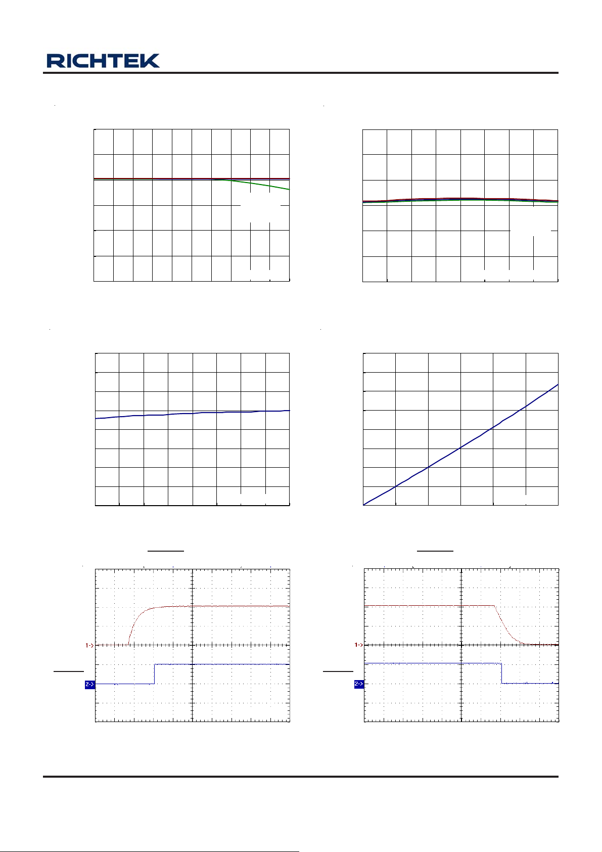
RESET
(1V/Div)
I
= 200mA
OUT
3.3 3.55 3.8 4.05 4.3 4.55 4.8 5.05 5.3
Inp ut Vol tag e (V)
RESET Power On
V
= 1V
DD4
200
150
100
Dropout Voltage (m V)
FB4
(200mV/Div)
RESET
(1V/Div)
50
V
0
0 50 100 150 200 250 300
OUT
Output Current (mA)
RESET Power Off
V
DD4
= 3V
= 1V
Time (5ms/Div)
Time (5ms/Div)
DS9912A-01 April 2011 www.richtek.com
9
Page 10

RT9912A
Application Information
RT9912A is a four-channel power ma nagement IC (PMIC)
including one step-up DC-DC converter (Boost), one stepdown DC-DC converter (Buck), one low dropout regulator
(LDO) and one voltage detector. For optimizing the
application of porta ble hand-held system with one or two
alkaline battery, several special logics are designed in
this chip. An extern al P-MOSFET is also needed for loaddisconnected function.
Step-Up DC-DC Converter (Boost)
The step-up DC-DC convert can start up even with the
input voltage a s low as 0.8V and operates with the input
voltage down to 0.7V. The cost of system is reduced by
the internal synchronous rectifier from eliminating an
external Schottky diode. The efficiency of light load is
improved by the pulse frequency modulation mode (PFM)
low quiescent current 30uA. The efficiency of heavy load
is also maintained by the internal synchronous rectifier
with resistance low to 0.2Ω.
The step-up DC-DC converter is designed as a
bootstrapped structure. As the chip is in the start-up period,
a low voltage start-up circuit will pull the output voltage to
a higher voltage (~1.5V). After the output voltage rea ches
a certain level, the main DC-DC circuitry will keep working
to pull the output voltage to the expected value set by
output divided resistor. The control scheme of the stepup DC-DC converter is pulse frequency modulation mode
(PFM) with constant-on-time a nd minimum-off-ti me. This
scheme can keep high efficiency during a wide loa d range.
An internal soft-start is also included in the step-up DCDC converter to limit the inrush current to less than a hal f
of the OCP level. As the ENBST is pulled low, the step-up
DC-DC converter will enter shutdown mode and all function
will be disabled.
As the ENSW is pulled high, the PSW will be pulled low
when the output of the step-up DC-DC converter is rea dy
(soft-start is finished). An extern al P-MOSFET is needed
to be a load-disconnected switch. The PSW is a signal
to control the external P-MOSFET. All loadings of the
system should be connected to the drain pin of the
P-MOSFET to prevent the step-up DC-DC converter startup in heavy load condition.
The maximum duty (D) of the step-up DC-DC converter is
around 50% so that the maximum output voltage is ideally
to be VIN / (1-D) = 2 x VIN. Actually, some voltage will
drop on the internal N-MOSFET and inductor . Therefore,
the maximum output voltage will be lower than the ideal
value and to be 2 x VIN.
The function of R9 and C14 is preventing the charge sharing
issue from the cap acitor in Q1's source pin to the ca pacitor
in Q1's drain pin. If the cap a citor in Q1's source pin is 10
times larger tha n the capacitor in Q1's drain pin, R9 and
C14 can be removed.
Step-Down DC-DC Converter (Buck)
The step-down DC-DC convert can reduce the cost of
system by the internal synchronous rectifier from
eliminating an external Schottky diode. The light load
efficiency is improved by the pulse frequency modulation
mode (PFM) and internal synchronous rectifier . For heavy
load, the efficiency is maintained by the internal
synchronous rectifier with the resistance low to 0.4Ω. The
control scheme of the step-down DC-DC converter is pulse
frequency modulation mode (PFM) with over-currentprotection (OCP) and minimum-off-ti me. This scheme can
keep high efficiency during a wide load ra nge. An internal
soft-start is also included in the step-down DC-DC
converter to limit the inrush current less than a half of
OCP level.
This step-down converter can operate in low-drop mode
and its output voltage depends on the voltage drop cross
the internal P-MOSFET and inductor . Normally , the value
is near VDD2 as the ESR of inductor is 0.1Ω and 60mA
loading. The minimum output voltage is 0.6V, which is
decided by the operation range of the internal circuit.
Low Dropout Regulator (LDO)
The low dropout regulator can regulate the output voltage
by setting the external resistor of FB3. An internal
compensation structure is designed for keeping stability
as wide range output capacitor and wide range loading.
The voltage detector is a comparator with reference to
detect the voltage of FB4.
10
DS9912A-01 April 2011www.richtek.com
Page 11

RT9912A
The maximum output voltage for LDO depends on the
voltage drop cross the internal P-MOSFET . Normally , the
value is (V DD3 − 0.4V) a s 200mA loading. The mini mum
output voltage is 1.6V, which is decided by the working
range of the internal circuit.
Output Voltage Setting
The regulated output voltage can be calculated following
formula :
R1
V = V 1
OUT FB
⎛⎞
×+
⎜⎟
R2
⎝⎠
To place the resistor-divider as close as possible to chip
can reduce noise sensitivity.
Voltage Detector
The RT9912A integrates a voltage detector with push-pull
output. The voltage detector senses V DD3V3_IO through
a resistor divider and compares it with internal 0.3V
reference voltage. When the sensed voltage is lower than
the reference voltage, the RESET pin output logic low
signal for system access. Connecting a capacitor from
the CT pin to GND ca n set the detect delay time a ccording
to Figure 1.
CH4 Detecter Delay Time
120
100
Inductor Selection
To select suitable inductance value is very important for
optimal performance. For boost converter, the control
method is constant on time and minimum off time. If the
inductance is low, it will cause effects of high in ductor
current and high output voltage ripple. The inductance value
can be calculated by following f ormula.
L
MIN
Where L
V
IN(MAX)
VT
IN(MAX) ON
≥
= minimum inductance
MIN
= maximum input voltage
V
LIM(MIN)
×
TON = 0.75us
I
LIM(MIN)
= 0.8A
A 4.7uH inductor is recommended f or typical a pplication.
For buck converter, a 4.7uH inductor is recommended
when VIN is less than 2.6V.
In addition, make sure the inductor saturation current
rating should be greater than the inductor pea k current.
Input Capacitor Selection
For better input bypa ssing, low-ESR ceramic ca pa citor is
recommended for better performance. A 10uF input
ca pacitor is suff icient and it is flexible to reduce the value
for a lower output power requirement.
80
60
Output Capacitor Selection
For lower output voltage ripple, low-ESR cera mic capa citor
is recommended. The output voltage ripple consists of
40
Delay Time (ms)
20
0
0 102030405060708090100
Capacitance (nF)
Figure 1. Detector Delay T i me
two components : one is the pulsating output ripple current
flowing through the ESR, and the other is the ca pa citive
ripple caused by charging and discharging.
For ceramic capacitor, the voltage ripple value is
approxi mated by :
V V≅
RIPPLE RIPPLE_C
For boost converter, calculate the minimum output
cap acita nce a s the following formula :
PEAK
2
11
L0.5I
≥
×
V
REPPLE_C
C
OUT
DS9912A-01 April 2011 www.richtek.com
Page 12

RT9912A
For buck converter, calculate the minimum output
cap acita nce a s the following formula :
I
⎛⎞
I1
OUT(MAX)
C
≥
OUT
fV
×
OUT(MAX)
×−
⎜⎟
I
PEAK
⎝⎠
REPPLE_C
THERMAL CONSIDERA TIONS
For continuous operation, do not exceed absolute
maximum operation junction temperature. The maximum
power dissipation depends on the thermal resistance of
IC package, PCB layout, the rate of surroundings airflow
and temperature difference between junction to a mbient.
The maximum power dissipation can be calculated by
following formula :
P
D(MAX)
= (T
J(MAX)
− TA) / θ
JA
2
2.0
1.8
1.6
1.4
1.2
1.0
0.8
0.6
0.4
0.2
Maximum Pow er Dissi pation (W )
0.0
0 25 50 75 100 125
Ambient Temper ature (°C)
WQFN-24L 4x4
Four Layers PCB
Figure 2. Derating Curves f or RT9912A Packages
Where T
temperature 125°C, T
θ
is the junction to ambient thermal resistance.
JA
is the maximum operation junction
J(MAX)
is the ambient te mperature and the
A
For recommended operating conditions specification of
RT9912A, where T
is the maximum junction
J(MAX)
temperature of the die (125°C) and TA is the maximum
ambient temperature. The junction to ambient thermal
resistance θJA is layout dependent. For WQFN-24L 4x4
packages, the thermal resistance θJA is 54° C/W on the
standard JEDEC 51-7 four layers thermal test board. The
maximum power dissipation at TA = 25°C can be calculated
by following formula :
P
= (125°C − 25°C) / (54°C/W) = 1.852W for
D(MAX)
WQF N-24L 4x4 pa ckages
The maximum power dissipation depends on operating
ambient temperature for fixed T
and thermal
J(MAX)
resistance θJA. For RT9912A packages, the Figure 2 of
derating curves allows the designer to see the effect of
rising ambient temperature on the maximum power
allowed.
Layout Considerations
For the best performance of the R T9912A, the f ollowing
PCB Layout guidelines must be strictly followed.
` Place the input and output capacitors as close as
possible to the input and output pins respectively for
good filtering.
` Keep the main power traces as possible as wide and
short.
` The switching node area connected to LX and inductor
should be minimized for lower EMI.
` Place the feedback components as close as possible
to the FB pin and keep these components away from
the noisy devices.
` Connect the GND a nd Exposed Pad to a strong ground
plane for maximum thermal dissipation and noise
protection.
12
DS9912A-01 April 2011www.richtek.com
Page 13

RT9912A
LX should be connected to inductor by
wide and short trace, keep sensitive
components away from trace.
PGND
GND
C1
VDD1
FB1
ENSW
PSW
NC
ENBST
C23C7
1
2
3
4
5
6
R8
V
OUT1
3.3V
GND
Q1
C6
VDD3V3_IO
C16
R1
GND
R7
C10
PGND
V
1.8V
PGND
OUT2
Place the feedback components as close
as possible to the FB pin and keep away
from noisy devices.
Input/Output capacitors must be placed
as close as possible to the Input/ Output
pins.
V
PGND
BAT
D1
24 2223
7
C5
L1
VOUT1
LX1
VBAT
21 20 19
GND
8 9 10 12
LX2
FB2
PVDD2 PGND1
PGND2
L2
C11
V
3.3V
11
OUT1
C4
CT
25
VDD2
GND
18
17
16
15
14
13
VOUT3
C9
C12
GND
R4
FB4
VDD4
RESET
ENBUK
VDD3
FB3
R6
GND
Connect the exposed
pad to a ground plane.
VDD3V3_IO
PGND
R3
VDD3V3_IO
C8
R5
C2
C3
PGND
V
OUT3
3.3V
PGND
Figure 3. PCB Layout Guide
DS9912A-01 April 2011 www.richtek.com
13
Page 14

RT9912A
Outline Dimension
D
E
A
A3
A1
D2
SEE DETAIL A
L
1
E2
1
2
be
DETAIL A
Pin #1 ID a nd T ie Bar Mark Option s
Note : The configuration of the Pin #1 identifier is optional,
1
2
but must be located within the zone indicated.
Dimensions In Millimeters Dimensions In Inches
Symbol
Min Max Min Max
A 0.700 0.800 0.028 0.031
A1 0.000 0.050 0.000 0.002
A3 0.175 0.250 0.007 0.010
b 0.180 0.300 0.007 0.012
D 3.950 4.050 0.156 0.159
D2 2.300 2.750 0.091 0.108
E 3.950 4.050 0.156 0.159
E2 2.300 2.750 0.091 0.108
e 0.500 0.020
L 0.350 0.450
Richtek Technology Corporation
Headquarter
5F, No. 20, Taiyuen Street, Chupei City
Hsinchu, Taiwan, R.O.C.
Tel: (8863)5526789 Fax: (8863)5526611
0.014 0.018
W-Type 24L QFN 4x4 Package
Richtek Technology Corporation
Taipei Office (Marketing)
5F, No. 95, Minchiuan Road, Hsintien City
Taipei County, Taiwan, R.O.C.
Tel: (8862)86672399 Fax: (8862)86672377
Email: marketing@richtek.com
Information that is provided by Richtek Technology Corporation is believed to be accurate and reliable. Richtek reserves the right to make any change in circuit
design, specification or other related things if necessary without notice at any time. No third party intellectual property infringement of the applications should be
guaranteed by users when integrating Richtek products into any application. No legal responsibility for any said applications is assumed by Richtek.
DS9912A-01 April 2011www.richtek.com
14
Page 15

 Loading...