

Richtek RT9819A-23GVL, RT9819A-24GVL, RT9819A-25GVL, RT9819A-27GV, RT9819A-27PV Schematic [ru]
...
Micro-Power Voltage Detectors
RT9819
General Description
The RT9819 is a micro-power voltage detector
supervising the power supply voltage level for
microprocessors (μP) or digital systems. It provides
internally fixed threshold levels with 0.1V per step ra nging
from 1.2V to 5V , which covers most digital applications. It
features low supply current of 3μA. The RT9819 performs
supervisory function by sending out a reset signal
whenever the V
voltage falls below a preset threshold
DD
level. This reset signal will last the whole period before
VDD recovering. Once VDD recovered upcrossing the
threshold level, the reset signal will be released after a
certain delay time. RT9819 is provided in SC-70-3,
SC-82 and SOT -23-3 packages.
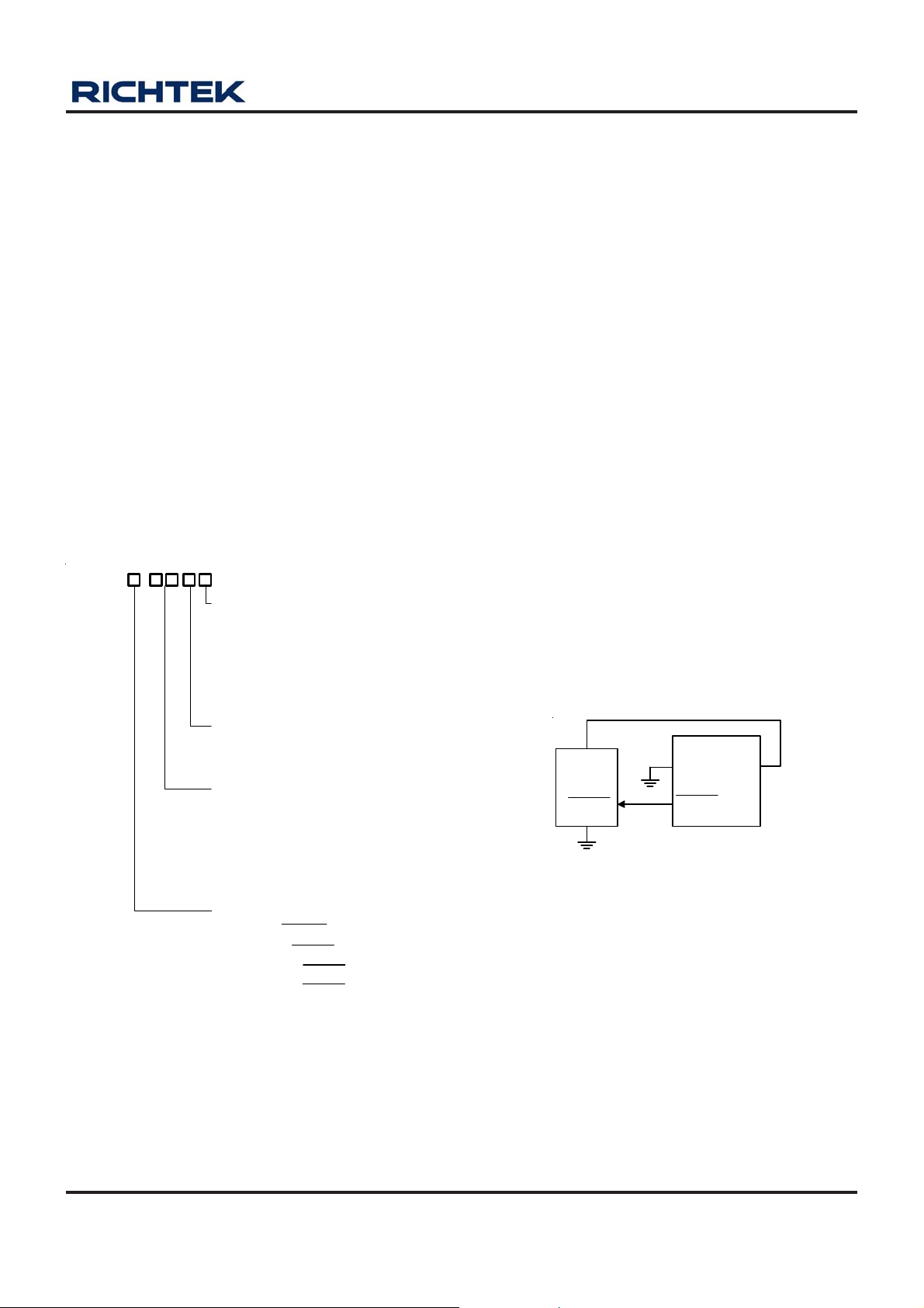
Ordering Information
RT9819
Note :
Richtek products are :
` RoHS compliant and compatible with the current require-
ments of IPC/JEDEC J-STD-020.
` Suitable for use in SnPb or Pb-free soldering processes.
Package Type
U3 : SC-70-3
V : SOT-23-3
VL : SOT-23-3 (L-Type)
Y : SC-82
YR : SC-82 (R-Type)
Lead Plating System
P : Pb Free
G : Green (Halogen Free and Pb Free)
Threshold Voltage
12 : 1.2V
13 : 1.3V
:
49 : 4.9V
50 : 5.0V
Reset Active Timeout Period
A = 0ms
(RESET)
B = 55ms (RESET)
C = 220ms (RESET)
D = 450ms (RESET)
E = 0ms (RESET)
F = 55ms (RESET)
G = 220ms (RESET)
H = 450ms (RESET)
Features
zz
Internally Fixed Threshold 1.2V to 5V in 0.1V Step
z
zz
zz
z High Accuracy
zz
zz
z Low Supply Current 3
zz
zz
z No External Components Required
zz
zz
z Quick Reset within 20
zz
zz
z Built-in Recovery Delay Include 0ms, 55ms, 220ms,
zz
±±
±1.5%
±±
μμ
μA
μμ
μμ
μs
μμ
450ms Options
zz
z Low Functional Supply Voltage 0.9V
zz
zz
z CMOS Push-Pull Output
zz
zz
z Small SC-70-3, SC-82 and SOT-23-3 Packages
zz
zz
z RoHS Compliant and 100% Lead (Pb)-Free
zz
Applications
z Computers
z Controllers
z Intelligent Instruments
z Critical μP and μC Power Monitoring
z Portable/Battery-Powered Equipment
Typical Application Circuit
VDD
up
RESET/
RESET
RT9819
VDDGND
RESET/
RESET
Marking Information
For marking information, contact our sales representative
directly or through a Richtek distributor located in your
area.
DS9819-07 April 2011 www.richtek.com
1
RT9819
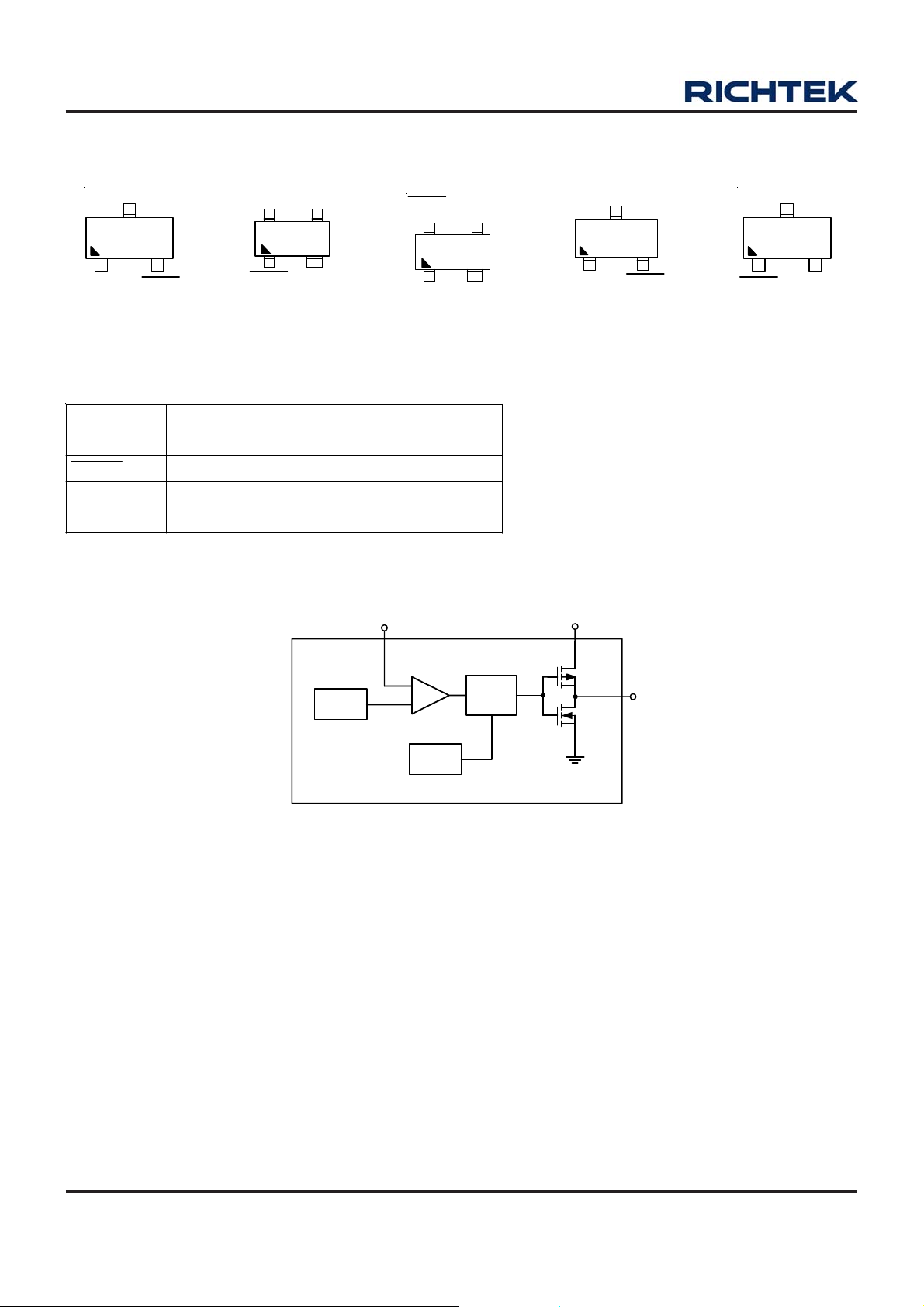
Pin Configurations
(TOP VIEW)
GND
VDD
3
2
RESET/
RESET
GND
4
RESET/
RESET
NC
3
2
VDD
Functional Pin Description
Pin Name Pin Function
GND Ground
RESET Active Low Push-Pull Reset Output
RESET Active High Push-Pull Reset Output
VDD Power Pin
Function Block Diagram
VDD
RESET/
RESET
4
VDD
NC
3
2
GND
VDD
GND
VDD
3
2
RESET/
RESET
RESET/
RESET
SOT-23-3 (L-Type)SOT-23-3SC-70-3 SC-82 (R-Type)SC-82
VDD
3
2
GND
VSET
Threshold
Voltage Setting
CMP
POR
Power On Reset
Timer
P MOS
N MOS
RESET/
RESET
DS9819-07 April 2011www.richtek.com
2
RT9819
Absolute Maximum Ratings (Note 1)
z T erminal V oltage (with Respe ct to GND)
VDD------------------------------------------------------------------------------------------------------------------------ −0.3V to 6.0V
z All Other Inputs -------------------------------------------------------------------------------------------------------- −0.3V to V
z Input Current, I
z Power Dissipation, PD @ T
----------------------------------------------------------------------------------------------------- 20mA
VDD
= 25°C
A
SC-70-3/SC-82 --------------------------------------------------------------------------------------------------------- 0.25W
SOT-23-3 ---------------------------------------------------------------------------------------------------------------- 0.4W
z Package Thermal Resistance (Note 2)
SC-70-3/SC-82, θJA--------------------------------------------------------------------------------------------------- 400°C /W
SOT-23-3, θJA----------------------------------------------------------------------------------------------------------- 250°C /W
z Lead Te mperature (Soldering, 10sec.)---------------------------------------------------------------------------- 260°C
z Storage T emperature Range ---------------------------------------------------------------------------------------- −65°C to 125°C
z ESD Susceptibility (Note 3)
HBM (Human Body Mode) ------------------------------------------------------------------------------------------ 2kV
MM (Ma chine Mode)-------------------------------------------------------------------------------------------------- 200V
Recommended Operating Conditions (Note 4)
DD
+0.3V
z Junction T emperature Range---------------------------------------------------------------------------------------- −40°C to 125°C
z Ambient T emperature Range---------------------------------------------------------------------------------------- −40°C to 85°C
Electrical Characteristics
(VDD = 3V, TA = 25°C, unless otherwise specified)
Parameter Symbol Test Conditions Min Typ Max Units
Operati ng VDD (V
) Range VDD
OUT
Supply Current IDD V
Reset Threshold VTH -- 1.2 to 5.0 -- V
Threshold Voltage Accuracy ΔVTH −1.5 -- +1.5 %
Threshold Voltage Hysteresis V
HYS
VDD Drop to Reset Delay tRD Drop = VTH −125mV -- 20 -- μs
RT9819A/E
Reset Active
Time Out Period
RT9819B/F 35 55 75 ms
VDD ≥ 1.02 × VTH
t
RT9819C/G 143 220 297 ms
RP
RT9819D/H 292 450 608 ms
RESET Outp ut Voltage Low
V
OL
RT9819A/B/C/D 0.9 -- 6
V
RT9819E/F/G/H 1.1 -- 6
= 3V , VDD = 4.5V -- 3 8 μA
TH
-- 0.01 VTH -- V
-- 0 -- ms
V
< V
DD
≥ 3V
V
TH
VDD < V
≥ 1.8V
V
TH
V
TH(MIN)
= 0.5mA
I
SINK
TH(MIN)
TH(MIN)
,I
SINK
,I
SINK
> VDD > 1V,
= 3.5mA,
= 1.2mA,
-- -- 0.4
-- -- 0.3
-- -- 0.3
V
To be continued
DS9819-07 April 2011 www.richtek.com
3
RT9819
Parameter Symbol Test Conditions Min Typ Max Units
V
> V
DD
TH(MAX)
RESET Output Voltage High
V
OH
RESET Output Voltage Low VOL
RESET Output Voltage High VOH
I
SOURCE
VDD > V
I
SOURCE
VDD > V
I
SOURCE
V
V
VDD > V
V
VDD > V
V
1.1V < V
I
SOURCE
1.8V < VDD < V
I
SOURCE
DD
TH
TH
TH
= 800μA, V
TH(MAX)
= 500μA, V
TH(MAX)
= 200μA, V
> V
TH(MAX)
≥ 3V
TH(MAX)
≥ 1.8V
TH(MAX)
≥ 1.2V
DD
= 200μA
= 500μA
3V < VDD < V
I
SOURCE
Note 1. Stresses listed as the above “Absolute Maximum Ratings” may cause permanent damage to the device. These are for
stress ratings. Functional operation of the device at these or any other conditions beyond those indicated in the
operational sections of the specifications is not implied. Exposure to absolute maximum rating conditions for extended
periods may remain possibility to affect device reliability.
Note 2. θ
Note 3. Devices are ESD sensitive. Handling precaution is recommended.
Note 4. The device is not guaranteed to function outside its operating conditions.
is measured in the natural convection at TA = 25°C on a low effective thermal conductivity test board of
JA
JEDEC 51-3 thermal measurement standard.
= 800μA
< V
TH(MIN)
,
TH
,
TH
,
TH
,I
SINK
,I
SINK
,I
SINK
TH(MIN)
TH(MIN)
,
≥ 3V
≥ 1.8 V
≥ 1.1 V
= 3. 5mA ,
= 1. 2mA ,
= 0. 5mA ,
,
,
−1.5 -- --
V
DD
0.8 V
0.8 V
-- --
DD
-- --
DD
-- -- 0.4
-- -- 0.3
-- -- 0.3
0.8 V
0.8 V
V
DD
-- --
DD
-- --
DD
−1.5 -- --
V
V
V
DS9819-07 April 2011www.richtek.com
4
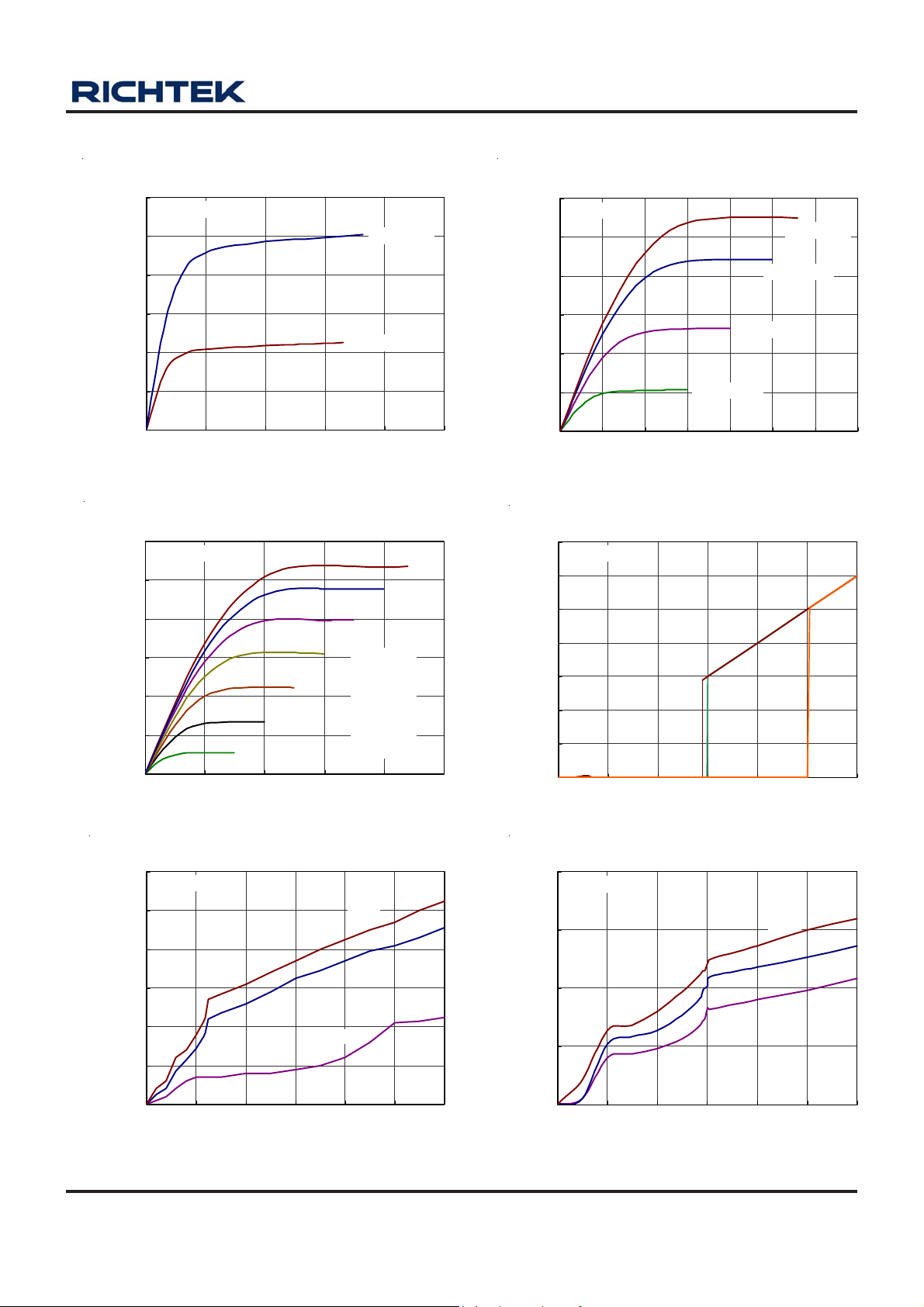
Typical Operating Characteristics
RT9819
Nch Driver Out put Curre nt vs. V
2.4
RT9819A-12
2
1.6
1.2
V
0.8
DD
Output Current (mA)
0.4
0
0 0.3 0.6 0.9 1.2 1.5
VDS (V)
Nch Driver Output Current vs. V
120
RT9819A-45
100
80
60
40
Output C urrent (mA)
20
VDD = 4.4V
= 4.0V
= 3.5V
= 3.0V
= 2.5V
= 2.0V
= 1.5V
V
DD
= 1.0V
DS
= 1.1V
DS
Nch Driver Output Current vs. V
60
RT9819C-30
V
= 2.8V
V
DD
= 2.0V
DD
= 2.5V
50
40
30
20
Output Current (mA)
10
0
00.511.522.533.5
V
DD
V
= 1.5V
DD
VDS (V)
Output Voltage vs. Input Voltage
7
RT9819A
6
5
4
3
2
Output V oltage (V)
1
2.9V
3.0V
DS
5.0V
0
012345
VDS (V)
Supply Current vs. Input Voltage
6
RT9819A-12
5
4
3
2
Supply Current (uA)
1
0
0123456
Inpu t Voltage (V)
80°C
25°C
-30°C
0
0123456
Inp ut Voltag e (V)
Supply Current vs. Input Voltage
4
RT9819C-30
3
2
1
Supply Current IDD (uA)
0
0123456
Inpu t Voltage (V)
80°C
25°C
-30°C
DS9819-07 April 2011 www.richtek.com
5
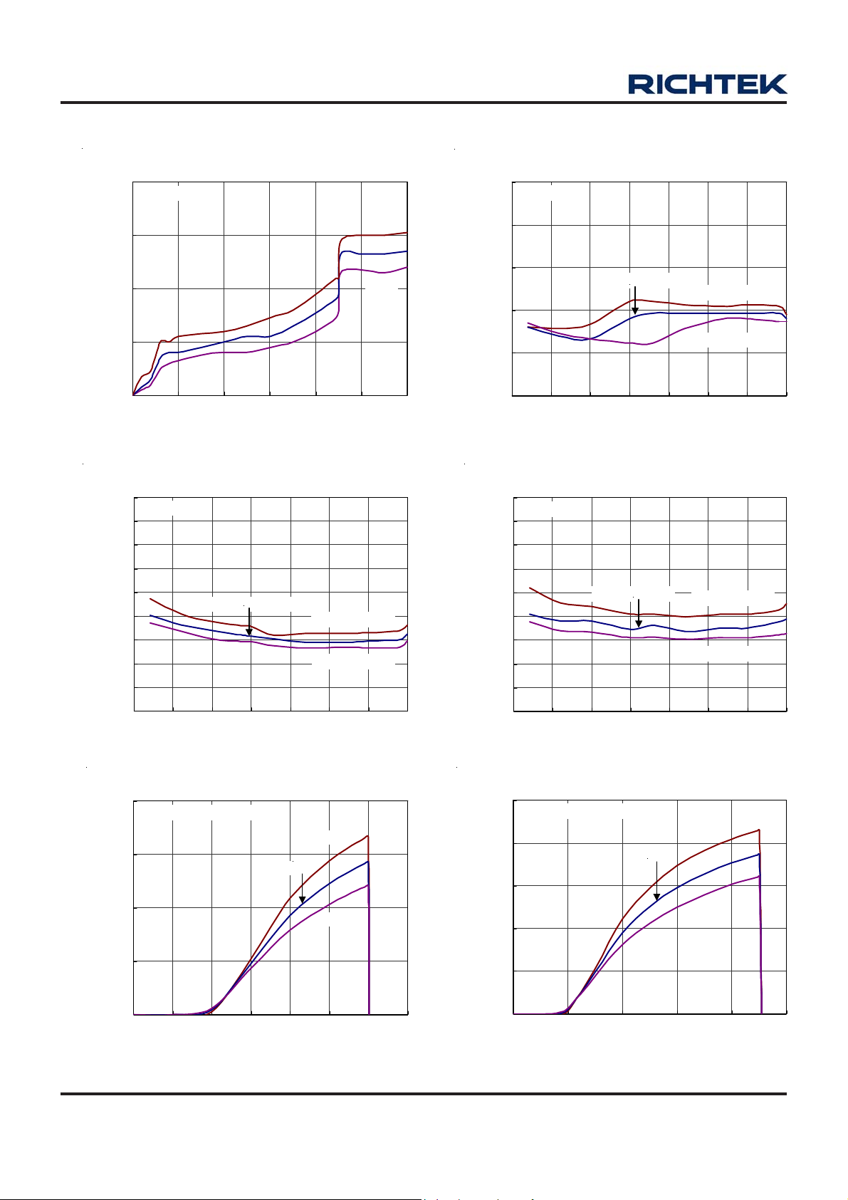
RT9819
Supply C ur re nt vs. Input Voltage
4
RT9819A-45
80°C
3
2
1
Supply Current (uA)
0
0123456
25°C
-30°C
Input Voltage (V )
Power-Down Reset Delay vs. Temperature
45
RT9819C-30
40
35
30
25
20
15
10
5
Power-Down Reset Delay ( us)
0
-50 -25 0 25 50 75 100 125
V
= 200mV
DROP
Temperature
(°C)
V
V
DROP
DROP
= 150mV
= 250mV
Power-Down Reset Delay vs. Temperatu re
15
RT9819A-12
12
9
6
3
V
DROP
= 200mV
V
V
DROP
DROP
= 150mV
= 250mV
Power-Down Reset Delay (us)
0
-50-25 0 25 50 75100125
Temperature
(°C)
Power-Down Reset Delay vs . Tem perature
45
RT9819A-45
40
35
30
V
25
20
15
10
5
Power-Down Reset Delay (us)
0
-50 -25 0 25 50 75 100 125
= 200mV
DROP
Temperature
(°C)
V
V
DROP
DROP
= 150mV
= 250mV
Nch Driver Sink C urrent vs. Input Voltage
40
RT9819C-30, V
30
(mA)
SINK
20
10
Sink Cur rent I
0
00.511.522.533.5
= 0.5V
DS
25°C
Input Vol tage ( V )
-30°C
80°C
Nch Driver Sink Current vs. Input Voltage
50
RT9819A-45, V
40
(mA)
30
SINK
20
10
Sink Cur rent I
0
012345
= 0.5V
DS
25°C
Input Voltage (V )
-30°C
80°C
DS9819-07 April 2011www.richtek.com
6
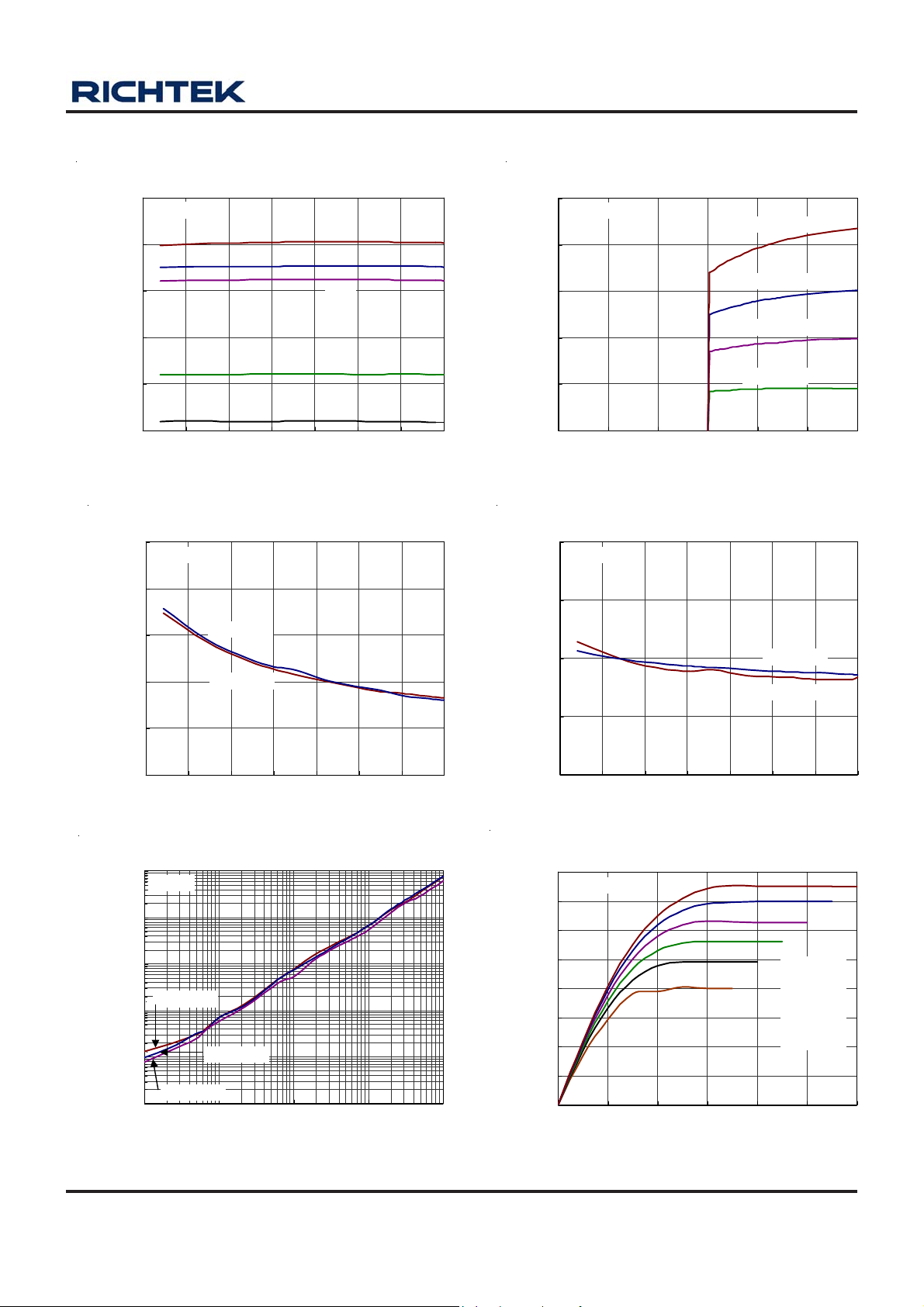
RT9819
Reset Threshold Deviation vs. Temperature
6.00
RT9819
5.0V
5.00
4.00
3.00
2.00
Reset Threshold Deviati on (V)
1.00
-50 -25 0 25 50 75 100 125
Temperature
4.5V
4.2V
2.2V
1.2V
(°C)
Power-Up Reset Time-Out vs. Temperature
500
RT9819C
400
V
= 2.9V
V
TH
TH
= 3.0V
300
200
100
Pch Driv er Output Current vs. Input Voltage
25
RT9819C-30
20
15
10
Output Current (mA)
5
0
0123456
VDS = 2.1V
VDS = 1.5V
VDS = 1.0V
VDS = 0.5V
Inpu t Voltage (V)
Power-Up Reset Time-Out vs. Temperature
100
RT9819A
(μs)
75
V
= 5.0V
V
TH
TH
= 4.5V
50
25
Power-Up Reset Time-Out ( m s)
0
-50 -25 0 25 50 75 100 125
Temperature
(°C)
Output Delay Time vs. Load Capacitance
1000
RT9819
100
10
V
= 3.0V
TH
1
V
= 2.9V
TH
TH
= 5.0V
Load Capacitance (uF)
0.1
Output Delay Time (ms)
0.01
V
0.0001 0.0010 0.0100 0.1000 1.0000
Power-Up Reset Time-Out (ms)
0
-50 -25 0 25 50 75 100 125
Temperature
(°C)
Nch Driver Output Current vs. V
160
RT9819G-31
140
120
100
80
60
40
20
Nch Driver Output Current (mA )
0
0123456
V
(V)
DS
VDD = 6.0V
= 5.5V
= 5.0V
= 4.5V
= 4.0V
= 3.5V
DS
DS9819-07 April 2011 www.richtek.com
7

RT9819
)
)
Nch Driver Output Current vs. Input Voltage
60
RT9819G-31
VDS = 0.5V
50
40
30
20
10
-30°C
25°C
80°C
Nch Driver Output Current (mA) 1
0
0123456
Inpu t Voltage (V)
Output Voltage vs. Input Voltage
7
RT9819G-31
6
5
4
3
2
Output Voltage (V)
1
0
0123456
Inpu t Voltage (V)
Power Down Reset Time-Out vs. Temperature
500
RT9819G-31
400
300
200
100
Power Down Reset Time-Out (ms
0
-50 -25 0 25 50 75 100 125
Temperature
(°C)
Power-Down Reset Time-Out vs. Tem perature
30
RT9819G-31
25
20
V
= 200mV
DROP
15
10
5
Power-Down Reset Time-Out (us
0
-50 -25 0 25 50 75 100 125
Temperature
V
V
(°C)
DROP
DROP
= 150mV
= 250mV
DS9819-07 April 2011www.richtek.com
8

RT9819
Application Information
Benefits of Highly Accurate Reset Threshold
Most μP supervisor ICs have reset threshold voltages between 1% and 1.5% below the value of nominal supply voltages.
This ensures a reset will not occur within 1% of the nominal supply, but will occur when the supply is 1.5% below
nominal.
DS9819-07 April 2011 www.richtek.com
9

RT9819
Outline Dimension
D
C
e
A
b
Dimensions In M illimeters Dimensions In Inches
Symbol
Min Max Min Max
A 0.800 1.100 0.031 0.044
A1 0.000 0.100 0.000 0.004
B 1.150 1.350 0.045 0.054
B
A1
H
L
b 0.150 0.400 0.006 0.016
C 1.800 2.450 0.071 0.096
D 1.800 2.250 0.071 0.089
e 1.300 0.051
H 0.080 0.260 0.003 0.010
L 0.210 0.460 0.008 0.018
SC-70-3 Surface Mount Package
10
DS9819-07 April 2011www.richtek.com
RT9819
D
e
C
b
A
e
Dimensions In Millimeters Dimensions In Inches
Symbol
Min Max Min Max
A 0.800 1.100 0.031 0.043
A1 0.000 0.100 0.000 0.004
B 1.150 1.350 0.045 0.053
B
b1
A1
H
L
b 0.150 0.400 0.006 0.016
b1 0.350 0.500 0.014 0.020
C 1.800 2.450 0.071 0.096
D 1.800 2.200 0.071 0.087
e 1.300 0.051
H 0.080 0.260 0.003 0.010
L 0.200 0.460 0.008 0.018
SC-82 Surface Mount Package
DS9819-07 April 2011 www.richtek.com
11

RT9819
D
C
e
A
b
B
A1
H
L
Dimensions In M illimeters Dimensions In Inches
Symbol
Min Max Min Max
A 0.889 1.295 0.035 0.051
A1 0.000 0.152 0.000 0.006
B 1.397 1.803 0.055 0.071
b 0.356 0.508 0.014 0.020
C 2.591 2.997 0.102 0.118
D 2.692 3.099 0.106 0.122
e 1.803 2.007 0.071 0.079
H 0.080 0.254 0.003 0.010
L 0.300 0.610 0.012 0.024
SOT-23-3 Surface Mount Package
Richtek Technology Corporation
Headquarter
5F, No. 20, Taiyuen Street, Chupei City
Hsinchu, Taiwan, R.O.C.
Tel: (8863)5526789 Fax: (8863)5526611
Richtek Technology Corporation
Taipei Office (Marketing)
5F, No. 95, Minchiuan Road, Hsintien City
Taipei County, Taiwan, R.O.C.
Tel: (8862)86672399 Fax: (8862)86672377
Email: marketing@richtek.com
Information that is provided by Richtek Technology Corporation is believed to be accurate and reliable. Richtek reserves the right to make any change in circuit design,
specification or other related things if necessary without notice at any time. No third party intellectual property infringement of the applications should be guaranteed
by users when integrating Richtek products into any application. No legal responsibility for any said applications is assumed by Richtek.
DS9819-07 April 2011www.richtek.com
12

 Loading...