

Richtek RT9818A-13PY, RT9818A-14PV, RT9818A-15PV, RT9818A-16PV, RT9818A-18GV Schematic [ru]
...
®
Micro-Power Voltage Detectors
RT9818
General Description
The RT9818 is a micro-power voltage detector supervising
the power supply voltage level for microprocessors (μP)
or digital systems. It provides internally fixed threshold
levels with 0.1V per step ranging from 1.2V to 5V, which
covers most digital applications. It features low supply
current of 3μA. The RT9818 performs supervisory function
by sending out a reset signal whenever the V
falls below a preset threshold level. This reset signal will
last the whole period before VDD recovering. Once V
recovered upcrossing the threshold level, the reset signal
will be released after a certain delay time. RT9818 is
provided in SC-82, SC-70-3, SOT-23-3, SOT-23-5 and
voltage
DD
DD
Features
zz
Internally Fixed Threshold 1.2V to 5V in 0.1V Step
z
zz
zz
z High Accuracy
zz
zz
z Low Supply Current 3
zz
zz
z No External Components Required
zz
zz
z Quick Reset within 20
zz
zz
z Built-in Recovery Delay Include 0ms, 55ms, 220ms,
zz
450ms Options
zz
z Low Functional Supply Voltage 0.9V
zz
zz
z N-Channel Open-Drain Output
zz
zz
z Small SC-82, SC-70-3, SOT-23-3, SOT-23-5, SOT-89
zz
Packages
zz
z RoHS Compliant and 100% Lead (Pb)-Free
zz
±±
±1.5%
±±
μμ
μA
μμ
μμ
μs
μμ
SOT-89 packages.
Applications
Ordering Information
RT9818
Note :
Richtek products are :
` RoHS compliant and compatible with the current require-
ments of IPC/JEDEC J-STD-020.
` Suitable for use in SnPb or Pb-free soldering processes.
Copyright 2013 Richtek Technology Corporation. All rights reserved. is a registered trademark of Richtek Technology Corporation.
DS9818-10 May 2013 www.richtek.com
Package Type
U3 : SC-70-3
V : SOT-23-3
VL : SOT-23-3 (L-Type)
B : SOT-23-5
X : SOT-89
Y : SC-82
YR : SC-82 (R-Type)
Lead Plating System
P : Pb Free
G : Green (Halogen Free and Pb Free)
Threshold Voltage
12 : 1.2V
13 : 1.3V
:
49 : 4.9V
50 : 5.0V
Reset Active Timeout Period
A = 0ms
(RESET)
B = 55ms (RESET)
C = 220ms (RESET)
D = 450ms (RESET)
E = 0ms (RESET)
F = 55ms (RESET)
G = 220ms (RESET)
H = 450ms (RESET)
©
z Computers
z Controllers
z Intelligent Instruments
z Critical μP and μC Power Monitoring
z Portable/Battery-Powered Equipment
Marking Information
For marking information, contact our sales representative
directly or through a Richtek distributor located in your
area.
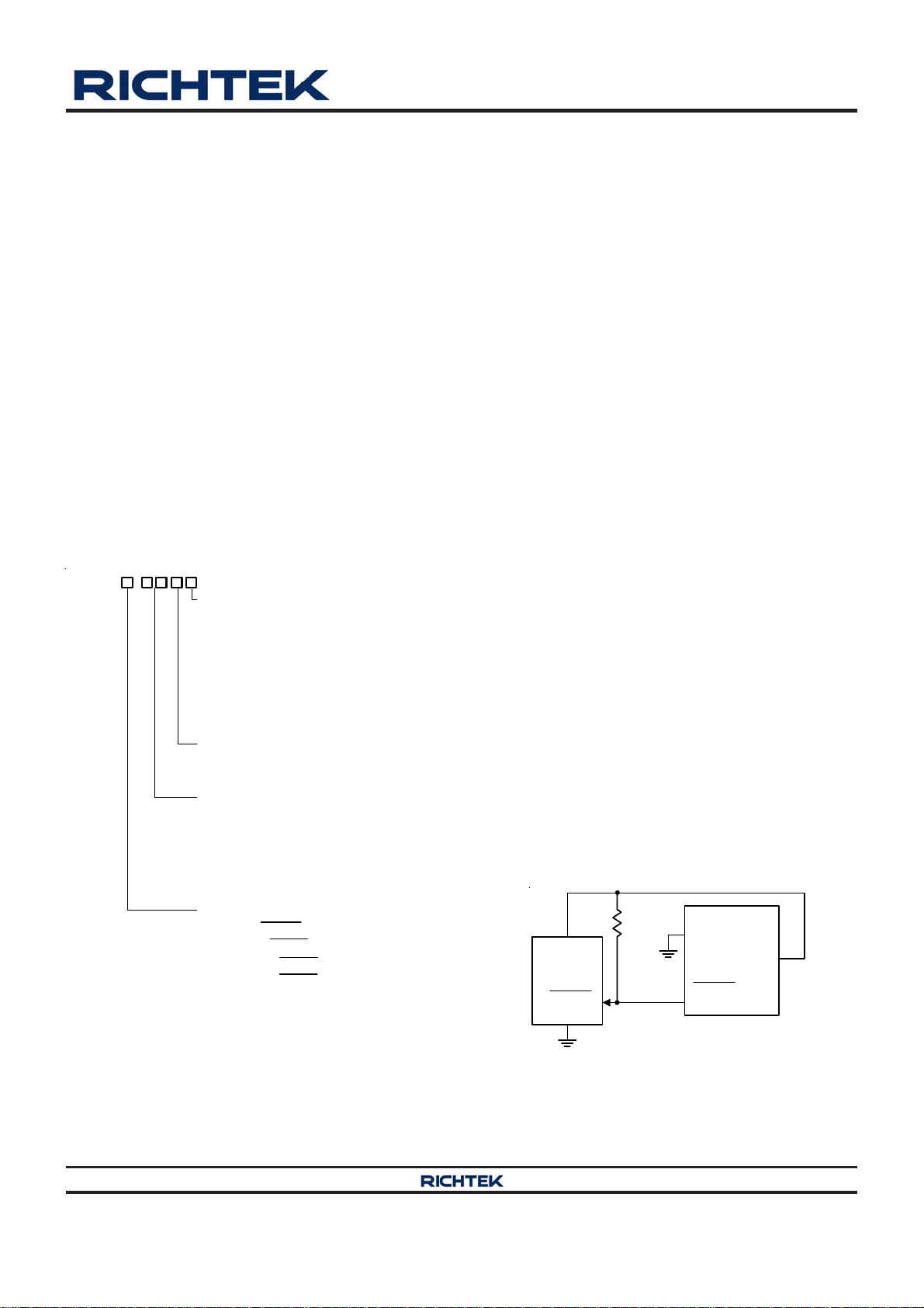
Typical Application Circuit
100k
Pull Up
VDD
μP
RESET/
RESET
RT9818
GND
VDD
RESET/
RESET
1
RT9818
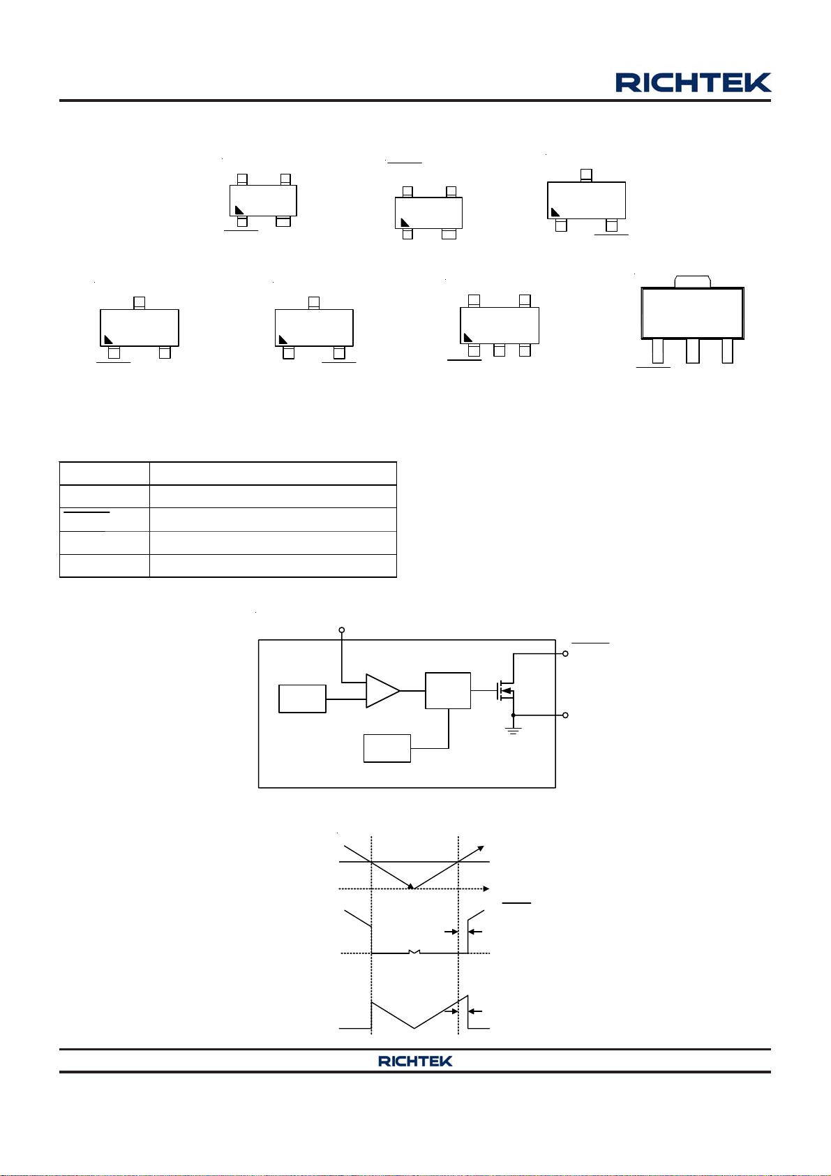
Pin Configurations
GND
RESET/
RESET
VDD
3
2
RESET/
RESET
GND
SOT-23-3
Functional Pin Description
Pin Name Pin Function
GND Ground
RESET Active Low Open-Drain Reset Output
RESET Active High Open-Drain Reset Output
NC
4
3
2
VDD
SC-82
VDD
GND
SOT-23-3 (L-Type)
3
2
RESET/
RESET
(TOP VIEW)
RESET/
RESET
VDD
SC-82 (R-Type)
NC
4
3
2
GND
RESET/
RESET
NC
5
NC
4
23
GND
VDD
GND
SC-70-3
VDD
3
2
RESET/
RESET
RESET/
RESET
231
GNDVDD
SOT-89SOT-23-5
VDD Power Pin
Function Block Diagram
Threshold
Voltage Setting
Timing Diagram
VSET
VDD
CMP
POR
Power On Reset
Timer
RESET/
RESET
N MOS
GND
V
DD
V
TH
0V
V
RESET
Delay Time (0, 55, 220, 450ms)
0V
V
RESET
Delay Time (0, 55, 220, 450ms)
0V
Copyright 2013 Richtek Technology Corporation. All rights reserved. is a registered trademark of Richtek Technology Corporation.
©
DS9818-10 May 2013www.richtek.com
2
RT9818
Absolute Maximum Ratings (Note 1)
z Terminal Voltage (with Respect to GND)
VDD--------------------------------------------------------------------------------------------------------------------- −0.3V to 6V
z All Other Inputs ----------------------------------------------------------------------------------------------------- −0.3V to (V
z Input Current, I
z Power Dissipation, P
-------------------------------------------------------------------------------------------------- 20mA
VDD
@ TA = 25°C
D
SC-70 / SC-82------------------------------------------------------------------------------------------------------- 0.25W
SOT-23-3 ------------------------------------------------------------------------------------------------------------- 0.4W
SOT-23-5 ------------------------------------------------------------------------------------------------------------- 0.4W
SOT-89---------------------------------------------------------------------------------------------------------------- 0.55W
z Package Thermal Resistance (Note 2)
SC-70 / SC-82, θJA------------------------------------------------------------------------------------------------- 400°C/W
SOT-23-3, θJA-------------------------------------------------------------------------------------------------------- 250°C/W
SOT-23-5, θJA-------------------------------------------------------------------------------------------------------- 250°C/W
SOT-89, θJA---------------------------------------------------------------------------------------------------------- 180°C/W
z Lead Temperature (Soldering, 10sec.)------------------------------------------------------------------------- 260°C
z Storage Temperature Range ------------------------------------------------------------------------------------- −65°C to 150°C
z ESD Susceptibility (Note 3)
HBM (Human Body Model)--------------------------------------------------------------------------------------- 2kV
DD
+ 0.3V)
Recommended Operating Conditions (Note 4)
z Junction Temperature Range ------------------------------------------------------------------------------------- −40°C to 125°C
z Ambient Temperature Range ------------------------------------------------------------------------------------- −40°C to 85°C
Electrical Characteristics
(VDD = 3V, unless otherwise specified)
Parameter Symbol Test Conditions Min Typ Max Unit
Operating VDD (V
Supply Current IDD V
Reset Threshold VTH T
Threshold Voltage Accuracy ΔVTH T
VDD Drop to Reset Delay tRD Drop = VTH −125mV -- 20 -- μs
Reset Active
Time Out Period
RESET Output Voltage Low
(Note 5)
Hysteresis Width V
) Range VDD 0.9 -- 6 V
OUT
= 3V, VDD = 4.5V, TA = 27°C -- 3 8 μA
TH
= 27°C -- 1.2 to 5 -- V
A
= 27°C −1.5 -- 1.5 %
A
RT9818A/E -- 0 --
RT9818B/F 35 55 75
RT9818C/G 143 220 297
RT9818D/H
t
V
RP
≥ 1.02 x VTH
DD
292 450 608
3 = VDD < VTH I
V
OL
-- 0.01VTH 0.016VTH V
HYS
> 3.5mA -- -- 0.4 V
SINK
ms
Copyright 2013 Richtek Technology Corporation. All rights reserved. is a registered trademark of Richtek Technology Corporation.
DS9818-10 May 2013 www.richtek.com
©
3
RT9818
Note 1. Stresses beyond those listed “Absolute Maximum Ratings” may cause permanent damage to the device. These are
stress ratings only, and functional operation of the device at these or any other conditions beyond those indicated in
the operational sections of the specifications is not implied. Exposure to absolute maximum rating conditions may
affect device reliability.
Note 2. θ
is measured at T
JA
Note 3. Devices are ESD sensitive. Handling precaution is recommended.
Note 4. The device is not guaranteed to function outside its operating conditions.
Note 5. The voltage V
OL
through the pull-up resistor. For typical application (R=100kΩ), V
= 25°C on a low effective thermal conductivity single-layer test board per JEDEC 51-3.
A
can be calculated by VOL = VDD − Ir * R. Where R is the pull-up resistor and Ir is the current flowing
is less than 0.2V.
OL
Copyright 2013 Richtek Technology Corporation. All rights reserved. is a registered trademark of Richtek Technology Corporation.
©
DS9818-10 May 2013www.richtek.com
4
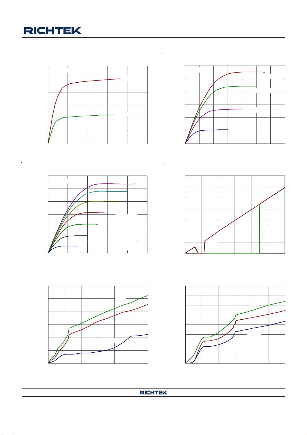
Typical Operating Characteristics
)
)
)
)
)
RT9818
Nch Driver Output Current vs. V
2.4
RT9818A-12
V
= 1.1V
2.0
1.6
1.2
0.8
Output Current (mA
0.4
0.0
0 0.3 0.6 0.9 1.2 1.5
DD
V
= 1V
DD
VDS (V)
Nch Driver Out put Current vs. V
120
RT9818A-45
100
80
60
40
Output Current (mA
20
0
012345
VDS (V)
VDD = 4.4V
= 4V
= 3.5V
= 3V
= 2.5V
= 2V
= 1.5V
DS
DS
Nch Driver Output Cu rrent vs. V
60
RT9818C-30
50
V
40
30
20
Output Current (mA
10
0
0 0.5 1 1.5 2 2.5 3 3.5
V
DD
= 1.5V
DD
V
= 2V
DD
V
DD
= 2.5V
DS
= 2.8V
VDS (V)
Output Voltage v s. Input Voltage
7
RT9818
6
5
4
3
2
Output Voltage (V)
1
0
0123456
1.2V
Input Voltage (V)
4.5V
Supply Current vs. Input Voltage
6
RT9818A-12
5
4
3
2
Supply Current (μA
1
0
0123456
80°C
25°C
−30°C
Input Voltage (V)
Copyright 2013 Richtek Technology Corporation. All rights reserved. is a registered trademark of Richtek Technology Corporation.
©
4.0
3.5
3.0
2.5
2.0
1.5
1.0
Supply Current (μA
0.5
0.0
Supply Current vs. Input Voltage
RT9818C-30
80°C
25°C
−30°C
0123456
Input Voltage (V)
DS9818-10 May 2013 www.richtek.com
5

RT9818
)
)
)
Supply Current vs . Input Voltage
4.0
RT9818A-45
3.5
3.0
2.5
2.0
1.5
1.0
Supply Current (μA
0.5
0.0
0123456
80°C
25°C
-30°C
Input Voltage (V)
Power Down Reset Delay vs. Temperature
45
RT9818C-30
40
35
30
Power Down Reset Delay vs. Temperature
14
RT9818A-12
12
10
8
6
4
2
Power Down Reset Delay (µs
0
-50 -25 0 25 50 75 100 125
V
DROP
= 200mV
V
V
DROP
DROP
= 150mV
= 250mV
Temperature (°C)
Power Down Reset Delay vs. Temperature
45
RT9818A-45
40
35
30
25
20
15
10
Power Down Reset Delay (µs
5
0
-50 -25 0 25 50 75 100 125
V
DROP
= 200mV
V
V
DROP
DROP
= 150mV
= 250mV
Temperature (°C)
Reset Threshold Deviation vs. Temperature
6
RT9818
5V
5
4
3
Reset Threshold (V)
2
1
-50 -25 0 25 50 75 100 125
Temperature (°C)
4.5V
4.2V
2.2V
1.2V
25
20
15
10
5
Power Down Reset Delay (µs) 1
0
-50-250 255075100125
V
DROP
= 200mV
V
V
DROP
DROP
= 150mV
= 250mV
Temperature (°C)
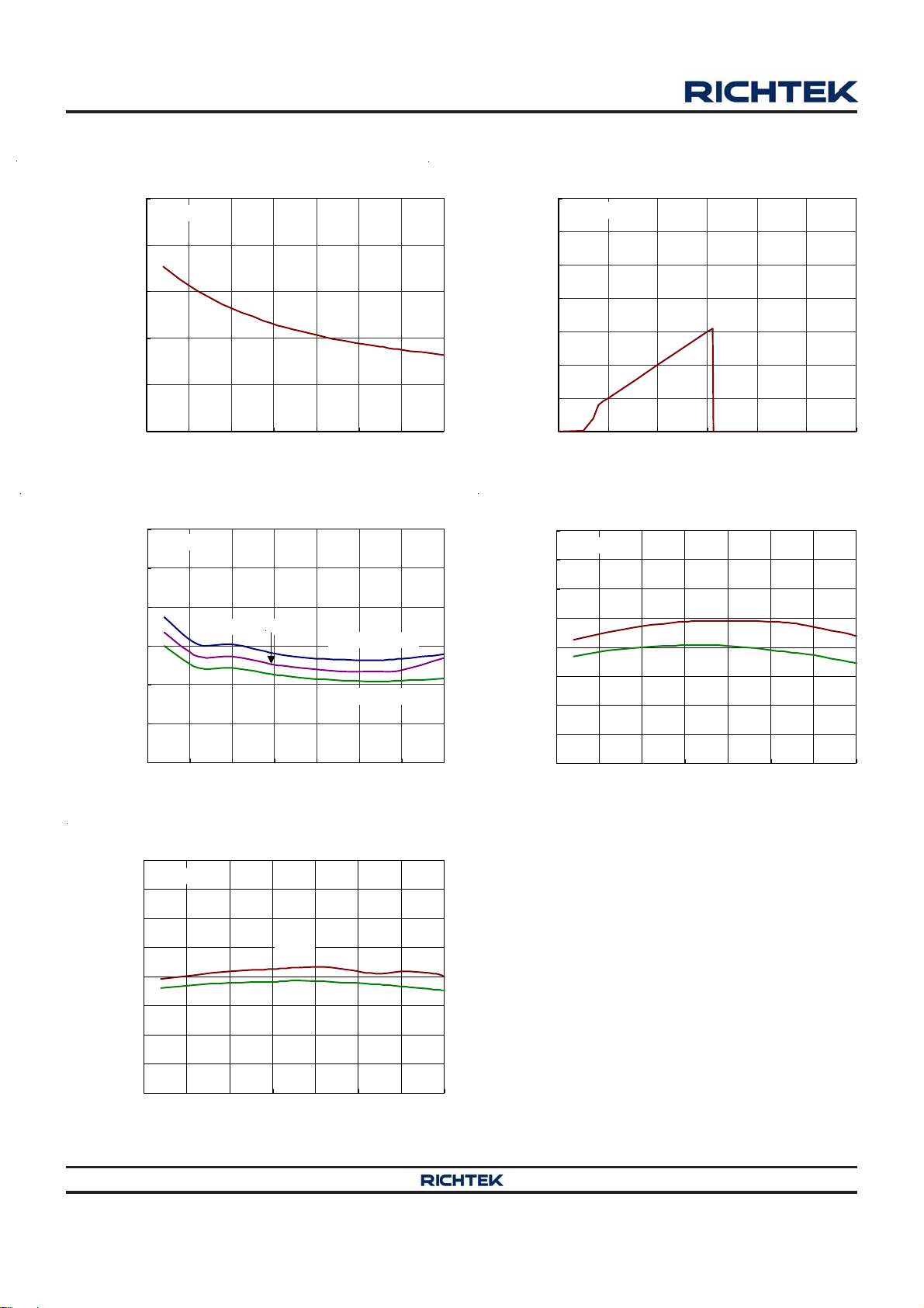
Nch Driver Sink Current vs. Input Voltage
40
RT9818C-30, V
35
30
(mA)
25
SINK
20
15
10
Sink Current I
5
0
0 0.5 1 1.5 2 2.5 3 3.5
= 0.5V
DS
25°C
Input Voltage (V)
−30°C
80°C
Copyright 2013 Richtek Technology Corporation. All rights reserved. is a registered trademark of Richtek Technology Corporation.
©
DS9818-10 May 2013www.richtek.com
6

RT9818
)
Nch Driver Sink Current vs. Input Voltage
50
RT9818A-45, V
40
DS
= 0.5V
−30°C
25°C
(mA)
30
SINK
80°C
20
Sink Current I
10
0
012345
Input Voltage (V)
Power Up Reset Time-Out vs. Temperature
100
RT9818A
80
60
V
= 5V
TH
40
V
TH
= 4.5V
Power Up Reset Time-Out vs. Temperature
500
RT9818C
400
V
= 2.9V
TH
300
200
100
V
= 3V
TH
Power Up Reset Time-Out (ms)
0
-50 -25 0 25 50 75 100 125
Temperature (°C)
Output Delay Time vs. Load Capacitance
1000
RT9818
100
10
V
= 1.2V
TH
1
0.1
20
Power Up Reset Time-Out (µs)
0
-50 -25 0 25 50 75 100 125
Temperature (°C)
Nch Driver Output Current vs. V
160
RT9818G-31
140
120
100
80
60
40
20
Nch Driver Output Current (mA) 1
0
0123456
VDS (V)
VDD = 6V
= 5.5V
= 5V
= 4.5V
= 4V
= 3.5V
DS
Output Delay Time (ms
V
= 4.5V
TH
0.01
0.0001 0.0010 0.0100 0.1000 1.0000
Load Capacitance (µF)
Nch Drive r Output Current vs. Input Voltage
60
RT9818G-31
VDS = 0.5V
50
40
30
20
10
Nch Driver Output Current (mA) 1
0
01234 56
Input Voltage (V)
−30°C
25°C
80°C
Copyright 2013 Richtek Technology Corporation. All rights reserved. is a registered trademark of Richtek Technology Corporation.
©
DS9818-10 May 2013 www.richtek.com
7
RT9818
)
)
Power Down Reset Time-Out vs. Temperature
500
RT9818G-31
400
300
200
100
Power Down Reset Time-Out (ms
0
-50 -25 0 25 50 75 100 125
Temperature (°C)
Power Down Reset Time-Out vs. Temperature
30
RT9818G-31
25
20
V
= 200mV
DROP
15
10
5
Power Down Reset Time-Out (µs
0
-50-250 255075100125
Temperature (°C)
V
V
DROP
DROP
= 150mV
= 250mV
Output Voltage v s . Input Voltage
7
RT9818G-31
6
5
4
3
2
Output Voltage (V)
1
0
0123456
Input Voltage (V)
Threshold Voltage vs. Temperature
4.40
RT9818A-42
4.35
4.30
4.25
4.20
4.15
4.10
Threshold Voltage (V) 1
4.05
4.00
-50-250 255075100125
Rising
Falling
Temperature (°C)
Threshold Voltage vs. Temperature
2.40
RT9818C-22
2.35
2.30
2.25
2.20
2.15
2.10
Threshold Voltage (V) 1
2.05
2.00
-50 -25 0 25 50 75 100 125
Copyright 2013 Richtek Technology Corporation. All rights reserved. is a registered trademark of Richtek Technology Corporation.
©
8
Rising
Falling
Temperature (°C)
DS9818-10 May 2013www.richtek.com

Application Information
Multiple Supplies
Mainly, the pull-up connected to the RT9818 will connect
to the supply voltage that is being monitored at the IC's
VDD pin. However, some systems may use the open-
drain output to level-shift from the monitored supply to
reset circuitry powered by some other supply.
Benefits of Highly Accurate Reset Threshold
Most μP supervisor ICs have reset threshold voltages
between 1% and 1.5% below the value of nominal supply
voltages. This ensures a reset will not occur within 1% of
the nominal supply, but will occur when the supply is 1.5%
below nominal.
RT9818
Copyright 2013 Richtek Technology Corporation. All rights reserved. is a registered trademark of Richtek Technology Corporation.
DS9818-10 May 2013 www.richtek.com
©
9
RT9818
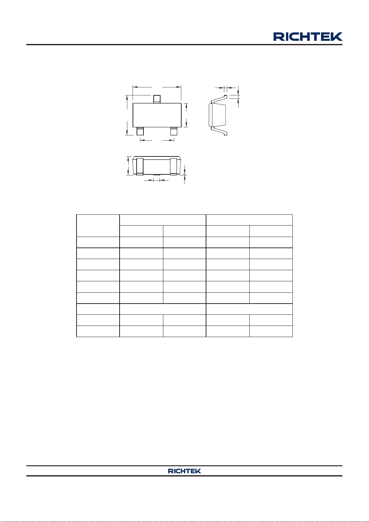
Outline Dimension
D
C
e
A
b
Dimensions In Millimeters Dimensions In Inch es
Symbol
Min Max Min Max
A 0.800 1.100 0.031 0.044
A1 0.000 0.100 0.000 0.004
B
A1
H
L
B 1.150 1.350 0.045 0.054
b 0.150 0.400 0.006 0.016
C 1.800 2.450 0.071 0.096
D 1.800 2.250 0.071 0.089
e 1.300 0.051
H 0.080 0.260 0.003 0.010
L 0.210 0.460 0.008 0.018
SC-70-3 Surface Mount Package
Copyright 2013 Richtek Technology Corporation. All rights reserved. is a registered trademark of Richtek Technology Corporation.
10
©
DS9818-10 May 2013www.richtek.com

RT9818
D
e
C
b
A
e
B
b1
A1
H
L
Dimensions In Millimeters Dimensions In Inches
Symbol
Min Max Min Max
A 0.800 1.100 0.031 0.043
A1 0.000 0.100 0.000 0.004
B 1.150 1.350 0.045 0.053
b 0.150 0.400 0.006 0.016
b1 0.350 0.500 0.014 0.020
C 1.800 2.450 0.071 0.096
D 1.800 2.200 0.071 0.087
e 1.300 0.051
H 0.080 0.260 0.003 0.010
L 0.200 0.460 0.008 0.018
SC-82 Surface Mount Package
Copyright 2013 Richtek Technology Corporation. All rights reserved. is a registered trademark of Richtek Technology Corporation.
DS9818-10 May 2013 www.richtek.com
©
11

RT9818
D
C
e
A
b
Dimensions In Millimeters Dimensions In Inch es
Symbol
Min Max Min Max
A 0.889 1.295 0.035 0.051
A1 0.000 0.152 0.000 0.006
B 1.397 1.803 0.055 0.071
b 0.356 0.508 0.014 0.020
B
A1
H
L
C 2.591 2.997 0.102 0.118
D 2.692 3.099 0.106 0.122
e 1.803 2.007 0.071 0.079
H 0.080 0.254 0.003 0.010
L 0.300 0.610 0.012 0.024
SOT-23-3 Surface Mount Package
Copyright 2013 Richtek Technology Corporation. All rights reserved. is a registered trademark of Richtek Technology Corporation.
12
©
DS9818-10 May 2013www.richtek.com

RT9818
H
D
L
C
b
A
e
Dimensions In Millimeters Dimensions In Inch e s
Symbol
Min Max Min Max
A 0.889 1.295 0.035 0.051
A1 0.000 0.152 0.000 0.006
B 1.397 1.803 0.055 0.071
b 0.356 0.559 0.014 0.022
C 2.591 2.997 0.102 0.118
D 2.692 3.099 0.106 0.122
B
A1
e 0.838 1.041 0.033 0.041
H 0.080 0.254 0.003 0.010
L 0.300 0.610 0.012 0.024
SOT-23-5 Surface Mount Package
Copyright 2013 Richtek Technology Corporation. All rights reserved. is a registered trademark of Richtek Technology Corporation.
DS9818-10 May 2013 www.richtek.com
©
13

RT9818
D
D1
A
C
e
e
A
b
b1
b
B
C1
H
Dimensions In Millimeters Dimensions In Inch es
Symbol
Min Max Min Max
A 1.397 1.600 0.055 0.063
b 0.356 0.483 0.014 0.019
B 2.388 2.591 0.094 0.102
b1 0.406 0.533 0.016 0.021
C 3.937 4.242 0.155 0.167
C1 0.787 1.194 0.031 0.047
D 4.394 4.597 0.173 0.181
D1 1.397 1.753 0.055 0.069
e 1.448 1.549 0.057 0.061
H 0.356 0.432 0.014 0.017
3-Lead SOT-89 Surface Mount Package
Richtek Technology Corporation
5F, No. 20, Taiyuen Street, Chupei City
Hsinchu, Taiwan, R.O.C.
Tel: (8863)5526789
Richtek products are sold by description only. Richtek reserves the right to change the circuitry and/or specifications without notice at any time. Customers should
obtain the latest relevant information and data sheets before placing orders and should verify that such information is current and complete. Richtek cannot
assume responsibility for use of any circuitry other than circuitry entirely embodied in a Richtek product. Information furnished by Richtek is believed to be
accurate and reliable. However, no responsibility is assumed by Richtek or its subsidiaries for its use; nor for any infringements of patents or other rights of third
parties which may result from its use. No license is granted by implication or otherwise under any patent or patent rights of Richtek or its subsidiaries.
DS9818-10 May 2013www.richtek.com
14

 Loading...