

Preliminary RT9801
User Programmable Micro-Power Voltage Detectors
General Description
The RT9801 is a micro-power voltage detector
supervising the power supply voltage level for
microprocessors (µP) or digital systems. It provides
user programmable threshold levels with 0.1V step
ranging from 1.5V to 5V, which covers most digital
applications. It features low supply current of 3µA.
Selection of V
is easily achieved through 3 pins
TH
connected to GND, VDD or floating for different
threshold voltage settings. Two versions of threshold
voltages, 1.5V ~ 4V and 2.5V ~ 5V, which are
programmed in factory are offered by customer
demands.
The RT9801 performs supervisory function by
sending out a reset signal whenever the VDD voltage
falls below a preset threshold level. This reset signal
will last the whole period before VDD recovering.
Reset signal will release after VDD is recovered and
lasts for the whole period of Reset Active Time-out
period.
RT9801 is N-channel, open-drain output and
provided in SOT-26 package.
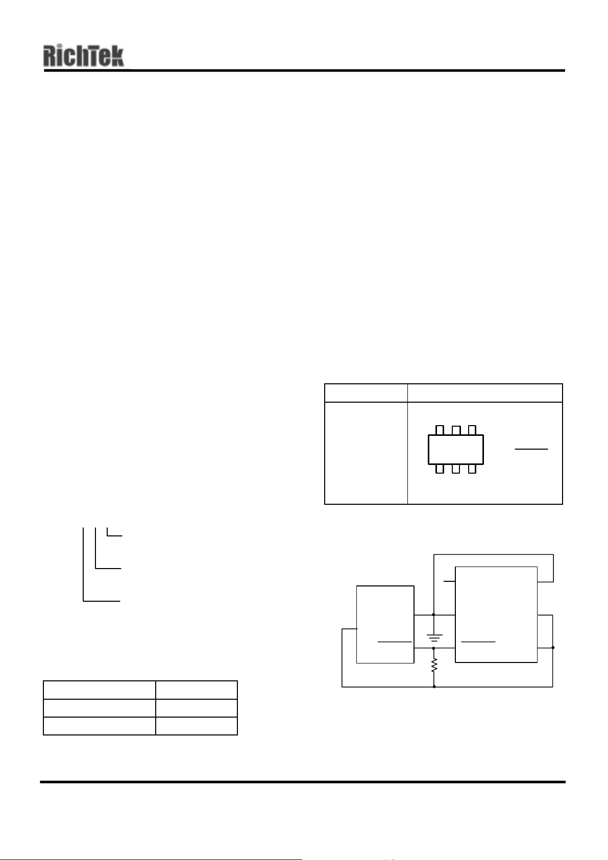
Ordering Information
Features
z User Programmable Threshold 1.5V to 5V in
0.1V Step with ±3% Accuracy
z Low Supply Current 3µA
z Quick Reset within 20µS
z Built-in Recovery Delay 200mS
z Low Functional Supply Voltage 0.9V
z Small SOT-26 Package
Applications
z Computers
z Controllers
z Intelligent Instruments
z Critical µP and µC Power Monitoring
z Portable/Battery-Powered Equipment
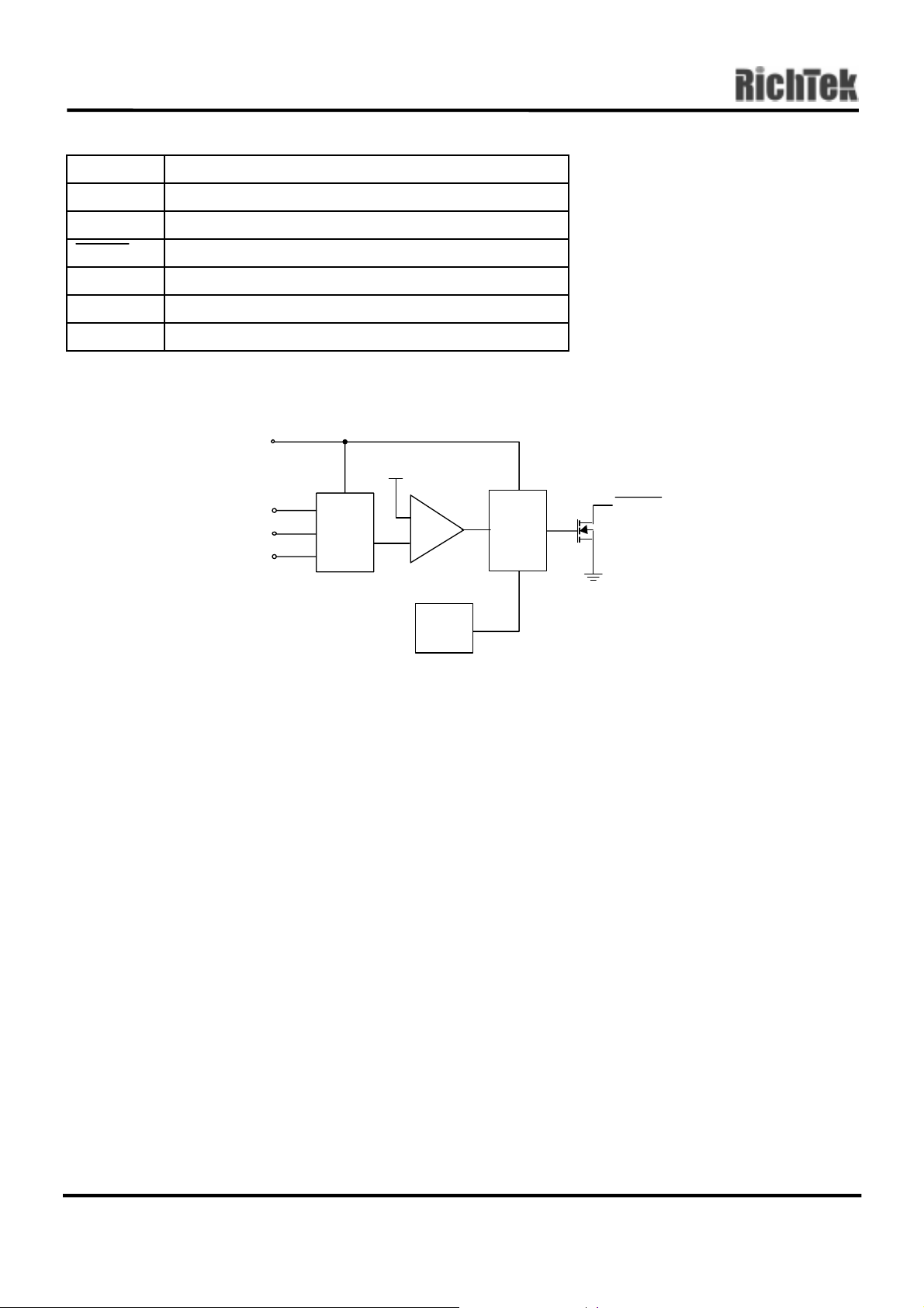
Pin Configurations
Part Number Pin Configurations
RT9801CE
(Plastic SOT-26)
64
5
321
TOP VIEW
1. VSET0
2. GND
3. RESET
4. VDD
5. VSET2
6. VSET1
RT9801
Typical Application Circuit
Package Type
E : SOT-26
Operating temperature range
C: Commercial standard
Reset Threshold
A : 2.5V~5V
B : 1.5V~4V
Marking Information
VDD
µP
GND
RESET
VSET0
GND
RESET
Pull Up
VSET1
RT9801
VSET2
VDD
Part Number Marking
RT9801ACE 1J
RT9 80 1B V
= 2.5V in this example
TH
RT9801BCE 1K
DS9801-02 August 2002 www.richtek.com
1
RT9801 Preliminary
Pin Description
Pin Name Pin Function
VSET0 Threshold Voltage Selection Pin 1
GND Ground Pin
RESET Reset Pulse Output, Negative Pulse
VDD Power Pin
VSET1 Threshold Voltage Selection Pin 2
VSET2 Threshold Voltage Selection Pin 3
Function Block Diagram
Inter nal Clock
VDD
VSET0
VSET1
VSET2
Threshold Vol tage Se t ting
VSET
CMP
POR
Power On Reset
TIMER
N
RESET
www.richtek.com DS9801-02 August 2002
2

Preliminary RT9801
Absolute Maximum Ratings
z Terminal Voltage (with Respect to GND)
VDD -0.3V to 6.0V
All Other Inputs -0.3V to VDD+0.3V
z Input Current, VDD 20mA
z Continuous Power Dissipation, P
@ TA = 25°C
D
SOT-26 0.25W
z Operating Junction Temperature Range -40°C ~ 125°C
z Storage Temperature Range -65°C ~ 125°C
z Package Thermal Resistance
SOT-26, θ
z Lead Temperature (Soldering, 5sec.) 260°C
JA
250°C /W
Electrical Characteristics
(VDD = 3V, unless specified)
Parameter Symbol Test Conditions Min Typ Max Units
Operating VDD (V
) Range V
OUT
Supply Current
Reset Threshold
Threshold Voltage Accuracy
VCC Drop to Reset Delay t
Reset Active Time Out Period
VSET Pin Input Threshold
RESET Output Voltage
I
DD
V
∆V
RD
t
RP
V
V
V
DD
TH
IL
IH
OL
0.9 -- 6 V
VDD = 1.5V ~ 3.5V, I
V
= 3.5V ~ 5V, I
DD
TA = 27°C
TA = 27°C
TH
OUT
OUT
= 0
= 0
-- -- 3
-- -- 3.3
-- Note1 -- V
-- -- 3 %
Drop = -125mV -- -- 20
VDD ≥ 1.02×VTH,
Programmable
TA = 27°C
TA = 27°C
V
< VTH, I
DD
SINK
= 3.5mA
-- 200 -- mS
--
--
-- 0.4 -- V
0.15V
0.85V
DD
DD
µA
µS
-V
--
DS9801-02 August 2002 www.richtek.com
3
RT9801 Preliminary
Note 1: Pin Conditions for Programmable Threshold Voltage Setting
RT9801A RT9801B Vset0 input Vset1 input Vset2 input
54VDDV
4.9 3.9 V
4.8 3.8 V
4.7 3.7 V
4.6 3.6 V
4.5 3.5 V
4.4 3.4 V
4.3 3.3 V
4.2 3.2 V
DD
DD
DD
DD
DD
DD
DD
DD
4.1 3.1 floating V
4 3 floating V
3.9 2.9 floating V
DD
V
DD
V
DD
floating V
floating floating
floating GND
GND V
GND floating
GND GND
DD
DD
DD
3.8 2.8 floating floating V
V
DD
floating
GND
DD
DD
V
DD
floating
GND
DD
3.7 2.7 floating floating floating
3.6 2.6 floating floating GND
3.5 2.5 floating GND V
DD
3.4 2.4 floating GND floating
3.3 2.3 floating GND GND
3.2 2.2 GND V
3.1 2.1 GND V
32GNDVDDGND
2.9 1.9 GND floating V
2.8 1.8 GND floating floating
2.7 1.7 GND floating GND
2.6 1.6 GND GND V
2.5 1.5 GND GND floating
VDD: bond to VDD; 0: bond to GND; f: no bonding
DD
DD
V
DD
floating
DD
DD
www.richtek.com DS9801-02 August 2002
4

Typical Operating Characteristics
Preliminary RT9801
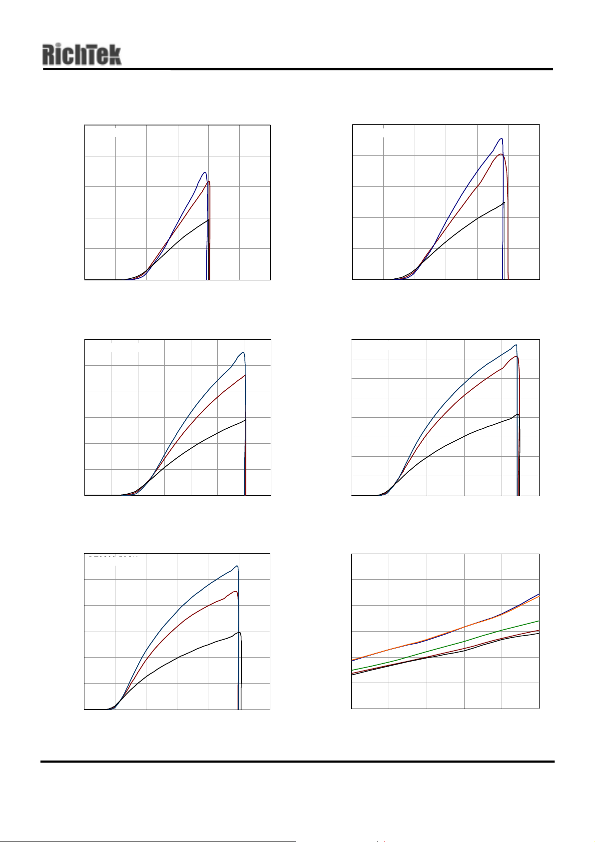
Nch Driver Output Current vs. V
7
6
5
(mA)
OUT
4
3
2
Output Current I
1
0
0 0.5 1 1.5 2 2.5 3
V
(V)
DS
T
= 25°C
RT9801-20CV
Nch Driver Output Current vs. V
18
2.8V
15
(mA)
12
OUT
9
2.0V
6
Output Current I
3
0
00.511.522.53
1.5V
VDS (V)
T
= 25°C
RT9801-30CV
DS
DS
Nch Driver Output Current vs. V
12
10
(mA)
8
OUT
6
4
Output Current I
2
0
00.511.522.53
1.5V
V
(V)
DS
2.0V
RT9801-24CV
Nch Driver Output Current vs. V
36
30
(mA )
24
OUT
18
2.5V
12
2.0V
Output Current I
6
0
01234
1.5V
RT9801-45CV
2.2V
T
3.0V
T
DS
= 25°C
DS
4.0V
3.5V
= 25°C
VDS (V)
Nch Driver output Current vs. V
40
32
(mA)
OUT
24
3.0V
16
8
Output Current I
1.5V
0
012345
2.5V
2.0V
RT9801-50CV
3.5V
4.0V
T
= 25°C
DS
4.5V
VDS (V)
Output Voltage vs. Input Voltage
7
T
= 25°C
6
(V)
5
OUT
4
3.0V
3
2
2.4V
2.0V
Output Voltage V
1
0
0.0 1.0 2.0 3.0 4.0 5.0 6.0
Input Voltage VIN (V)
5.0V
4.5V
DS9801-02 August 2002 www.richtek.com
5

RT9801 Preliminary
µ
µ
µ
µ
Supply Current vs. Input Voltage
4
3
( A)
SS
2
1
Supply Current I
0
0123456
80 C
25 C
-30 C
RT9808-20CV
RT9801-20CV
Input Voltage VIN (V)
Supply Current vs. Input Voltage
4
3
( A)
SS
2
80 C
25 C
-30 C
°
°
°
Supply Current vs. Input Voltage
4
3
( A)
SS
2
1
Supply Current I
0
0123456
80 C
25 C
-30 C
°
°
°
RT9808-24CV
RT9801-24CV
Input Voltage VIN (V)
Supply Current vs. Input Voltage
5
°
4
( A)
SS
3
2
80 C
°
25 C
°
-30 C
1
Supply Current I
RT9808-30CV
0
0123456
RT9801-30CV
Input Voltage VIN (V)
Supply Current vs. Input Voltage
5
°
80 C
4
°
( A)
SS
3
2
Supply Current I
1
0
0123456
Input Voltage VIN (V)
25 C
-30 C
°
RT9808-50CV
RT9801-50CV
Supply Current I
1
RT9808-45CV
0
0123456
RT9801-45CV
Input Voltage VIN (V)
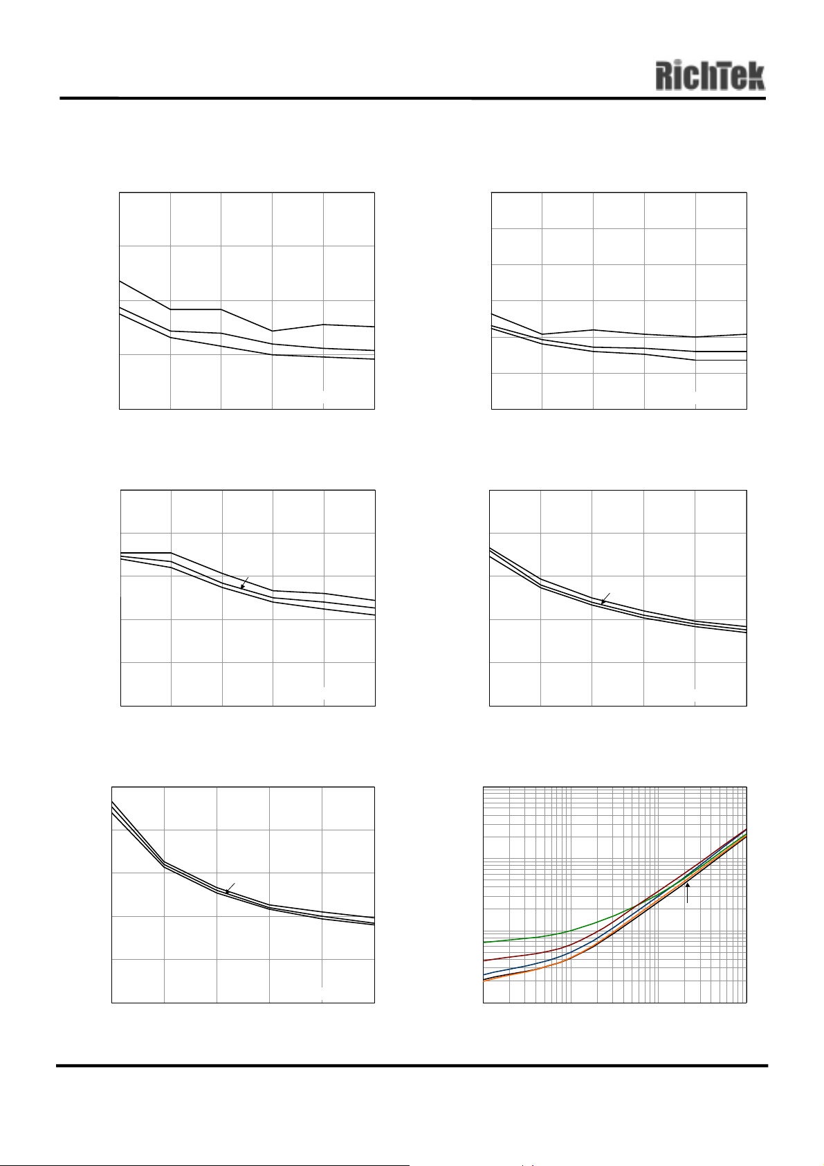
Reset Threshold Dev iation vs. Temp.
5.2
4.8
4.4
4
3.6
Threshold (V)
3.2
2.8
2.4
-40 -15 10 35 60 85
Temperature( C)
°
5.0V
4.5V
3.0V
2.5V
www.richtek.com DS9801-02 August 2002
6
Preliminary RT9801
Nch Driver Output Current vs. Input Voltage
10
RT9801-20CV
RT9808-20CV
V
= 0.5V
DS
8
°
(mA)
6
OUT
4
2
Output Current I
0
0 0.5 1 1.5 2 2.5 3
-30 C
25 C
°
80 C
°
Input Voltage VIN (V)
Nch Driver Output Current vs. Input Voltage
12
RT9801-30CV
RT9808-30CV
V
= 0.5V
DS
10
°
(mA)
OUT
Output Current I
8
6
4
2
-30 C
25 C
80 C
°
°
Nch Driver Ou tput Current vs. Input Voltage
10
RT9801-24CV
RT9808-24CV
= 0.5V
V
DS
8
(mA)
6
OUT
4
2
Output Current I
0
0 0.5 1 1.5 2 2.5 3
-30 C
25 C
80 C
Input Voltage VIN (V)
Nch Driver Output Current vs. Input Voltage
16
RT9801-45CV
RT9808-45CV
= 0.5V
V
DS
14
12
(mA)
10
OUT
Output Current I
8
6
4
2
-30 C
°
25 C
80 C
°
°
0
0 0.5 1 1.5 2 2.5 3 3.5
Input Voltage VIN (V)
Nch Driver Output Current vs. Input Voltage
18
RT9808-50CV
RT9801-50CV
V
= 0.5V
DS
15
(mA)
12
OUT
9
6
Output Current I
3
0
0123456
Input Voltage VIN (V)
-30 C
25 C
80 C
°
°
°
0
012345
Input Voltage VIN (V)
Power-Up reset Ti meou t vs. Temp.
350
300
250
200
150
100
Power-Up Reset Timeout (ms)
50
-40 -15 10 35 60 85
Tem perture ( C)
°
2V
2.4V
3V
4.5V
5V
DS9801-02 August 2002 www.richtek.com
7
RT9801 Preliminary
V
µ
µ
µ
µ
Power-Down Reset Delay vs. Temp.
4.0
3.0
2.0
V
drop
V
drop
1.0
Power-Down Reset Delay ( s)
0.0
-40 -15 10 35 60 85
V
drop
RT9801-20CV
RT9808-20CV
Tem perture ( C)
Power-Down Reset Delay vs. Temp.
1.5
1.2
= 200mV
V
0.9
drop
V
drop
= 150mV
= 200mV
= 250mV
= 150mV
Power-Down Reset Delay vs. Temp.
3.0
2.5
2.0
1.5
V
1.0
0.5
Power-Down Reset Delay ( s)
0.0
-40 -15 10 35 60 85
drop
V
drop
V
drop
RT9801-24CV
RT9808-24CV
Tem perture ( C)
Power-Down Reset Delay vs. T emp.
1.5
1.2
0.9
V
drop
= 200mV
= 150mV
= 200mV
= 250mV
0.6
0.3
V
drop
Power-Down Reset Delay ( s)
RT9801-30CV
0.0
-40 -15 10 35 60 85
RT9808-30CV
Tem perture ( C)
Power-Down Reset Delay vs. Temp.
1.5
1.2
0.9
0.6
0.3
Power-Down Reset Delay ( s)
0.0
-40 -15 10 35 60 85
Tem perture ( C)
V
drop
= 200mV
°
V
drop
V
drop
RT9801-50CV
RT9808-50CV
= 250mV
= 150mV
= 250mV
V
= 150mV
0.6
0.3
drop
V
drop
= 250mV
Power-Down Reset Delay ( s)
RT9801-45CV
0.0
-40 -15 10 35 60 85
RT9808-45CV
Tem perture ( C)
Output Delay Time vs. Load Capacitance
1000
(ms)
P
100
2.4
10
4.5V
5V
Output Delay Time t
2V
3V
1
0.0001 0.001 0.01 0.1
Load Capacitance C
OUT
T
(uF)
= 25°C
www.richtek.com DS9801-02 August 2002
8

Package Information
Preliminary RT9801
D
C
b
A
e
B
A1
Symbol
A 0.889 1.295 0.035 0.051
A1 -- 0.152 -- 0.006
Dimensions In Millimeters Dimensions In Inches
Min Max Min Max
H
L
B 1.397 1.803 0.055 0.071
b 0.356 0.559 0.014 0.022
C 2.591 2.997 0.102 0.118
D 2.692 3.099 0.106 0.122
e 0.838 1.041 0.033 0.041
H 0.102 0.254 0.004 0.010
L 0.356 0.610 0.014 0.024
SOT- 26 Surface Moun t Package
DS9801-02 August 2002 www.richtek.com
9

RT9801 Preliminary
RICHTEK TECHNOLOGY CORP.
Headquarter
5F, No. 20, Taiyuen Street, Chupei City
Hsinchu, Taiwan, R.O.C.
Tel: (8863)552678 9 Fax: (8863)5526611
www.richtek.com DS9801-02 August 2002
RICHTEK TECHNOLOGY CORP.
Taipei Office (Marketing)
8F-1, No. 137, Lane 235, Paochiao Road, Hsintien City
Taipei County, Taiwan, R.O.C.
Tel: (8862)891914 66 Fax: (8862)89191465
Email: marketing@richtek.com
10

 Loading...