

Page 1
Evaluation Board
RT9706
80m
ΩΩ
Ω, 500mA High-Side Power Switch with Flag
ΩΩ
General Description
The RT9706 is a cost-effective, low voltage, single
N-Channel MOSFET high-side power switch, optimized
for self-powered and bus-powered Universal Serial Bus
(USB) application s. The RT9706 equipped with a charge
pump circuitry to drive the internal MOSFET switch; the
switch's low R
requirements; and a flag output is available to indicate
fault conditions to the local USB controller.
Additional features include soft-start to limit inrush current
during plug-in, thermal shutdown to prevent catastrophic
switch failure from high-current loads, under-voltage
lockout (UVLO) to ensure that the device remains off
unless there is a valid input voltage present, lower
quiescent current as 25μA making this device ideal for
portable battery operated equipment.
IC Part Number
Board Number
, 80mΩ, meets USB voltage drop
DS(ON)
RT9706
RT9706 SOT-23-5_V0
Features
zz
z
Compliant to USB Specifications
zz
zz
z
Built-In (Typically 80m
zz
zz
z
Output Can Be Forced Higher than Input (Off-State)
zz
zz
z
Guaranteed 500mA Continuous Load Current
zz
zz
z
Wide Input Voltage Ranges : 2V to 5.5V
zz
zz
z
Open-Drain Fault Flag Output
zz
zz
z
Hot Plug-In Application (Soft-Start)
zz
zz
z
1.7V T ypical Under-Voltage Lockout (UVLO)
zz
zz
z Current Limiting Protection
zz
zz
z Thermal Shutdown Protection
zz
zz
z Reverse Current Flow Blocking (no body diode)
zz
zz
z UL Approved
zz
−−
−E219878
−−
ΩΩ
Ω) N-Channel MOSFET
ΩΩ
Applications
z USB Bus/Self Powered Hubs
z USB Peripherals
z ACPI Power Distribution
z PC Card Hot Swap
z Notebook, Motherboard PCs
z Battery-Powered Equipment
z Hot-Plug Power Supplies
z Battery-Charger Circuits
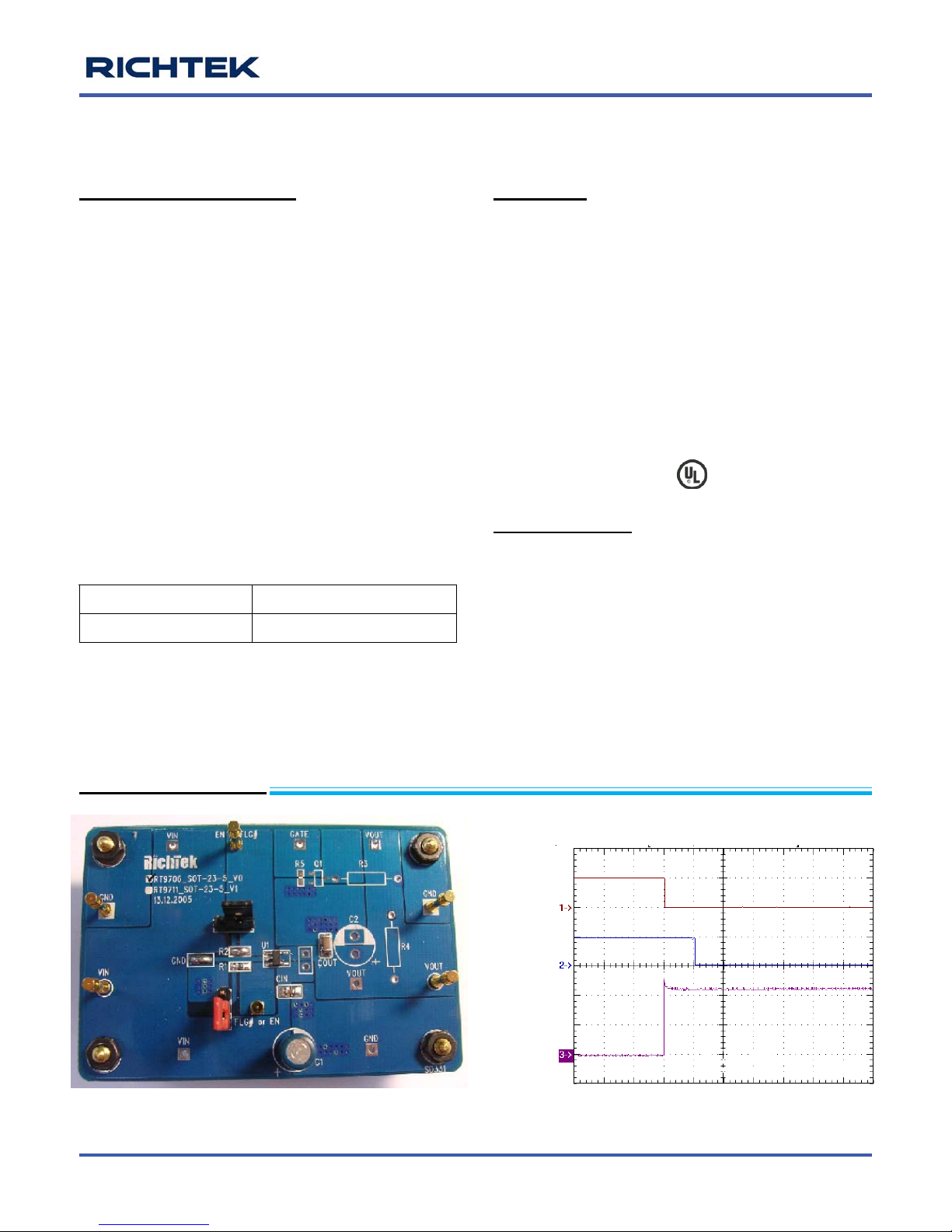
Evaluation Board
RT9706 SOT-23-5_V0
EVB9706-02 October 2007 www.richtek.com
V
EN
(5V/Div)
FLAG
(5V/Div)
I
OUT
(500mA/Div)
Flag Response
Time (10ms/Div)
R
= 0Ω
L
1
Page 2
RT9706
Evaluation Board
Specification
Parameter Symbol Min Typ Max Units
Operation Voltage Range VIN 2 5 5.5 V
Under-voltage Lockout V
Under-voltage Hysteresis ΔV
1.3 1.7 2.4 V
UVLO
-- 0.1 -- V
UVLO
Logic-Low Voltage VIL -- -- 0.8 V
EN Threshold
Logic-High Voltage V
Current Limit I
2.0 -- -- V
IH
0.5 -- 1.25 A
LIM
FLAG Delay Time tD 5 12 20 ms
Thermal Shutdown Protection TSD
Thermal Shutdown Hysteresis ΔTSD
-- 130 --
-- 20 --
°C
°C
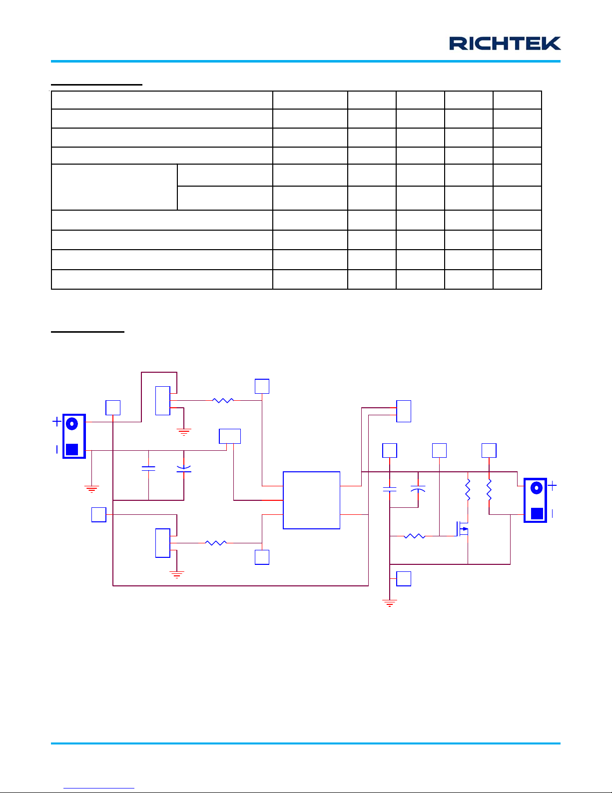
Schematic
/FLG or EN
Z8
2
1
/FLG
1
2
3
EN
1
Z9
EN or /FLG
RT9711 / RT9706
SOT-23 -5
/FLG
GND
EN
U1
VOUT
VDD
Z15
1
2
R3 R4
23
Q1
VOUTVOUT
Z12
1
Vout
VOUT
1
2
R5
Z10
GATE
1
C2
GATE
1
Z11
1
5
4
12
Cout
1
GND
VIN
1
2
VIN
VIN
Z6
VIN
Z5
1
1
3
2
1
Z14
Cin
1 2
3
2
1
Z13
C1
R1
R2
GND
Z7
1
2
Figure 1. EVB Circuit
EVB9706-02 October 2007www.richtek.com
Page 3

Evaluation Board
RT9706
Bill of Materials
Reference Qty Part Number Description Package Manufacture
U2 1 RT9706 High-Side Power Switch SOT-23-5 RichTek
Cin 1 CAP
Cout 1 CAP
C1 1 C
R1 1
Z13&Z14 1 SIP-3P Jumper Switch DIP
Z7 1 Short by solder
R2 0
C2 0 NC
R3 0
R4 0
R5 0
Q1 0 NC
R
1μF, Ceramic, ±10%, 16V, X5R
10μF, Ceramic, ±10%, 6.3V, X7R
33μF, Electrolytic, 50V
100KΩ, Resistor,
0Ω, Short by solder
NC
NC
NC
0603 PSA
0603 PSA
DIP
0603
PCB Layout
Figure 2. Top Layer Figure 3. Bottom Layer
Operating Guideline
1. Connect input power (2V< VIN < 5.5V) and in put ground to VIN a nd GND pins respectively.
2. Connect positive end and negative end of load to VOUT and GND pins respectively .
3. There is a jumper switch EN (at upper site). When the EN is set at LOW (<0.8), R T9706 will be turn on. To turn off the
RT9706, the EN should be set at HIGH (>2V).
EVB9706-02 October 2007 www.richtek.com
3
Page 4

RT9706
Evaluation Board
More Information
For more information, plea se find the related datasheet or application notes from RichTek website :
http://www.richtek.com
Richtek Technology Corporation
Headquarter
5F, No. 20, Taiyuen Street, Chupei City
Hsinchu, Taiwan, R.O.C.
Tel: (8863)5526789 Fax: (8863)5526611
4
Richtek Technology Corporation
Taipei Office (Marketing)
8F, No. 137, Lane 235, Paochiao Road, Hsintien City
Taipei County, Taiwan, R.O.C.
Tel: (8862)89191466 Fax: (8862)89191465
Email: marketing@richtek.com
EVB9706-02 October 2007www.richtek.com
 Loading...