

Page 1
Preliminary
RT9224C
VRM 9.0 Synchronous PWM Buck Converter
Controller and Output Voltage Monitor
General Description
The RT9224C is a high speed switching controller
designed for use in Synchronous DC/DC buck
converter for modern CPUs. The regulated output
voltage is digitally programmable from 1.075V to
1.85V by a 5-bit DAC which provides initial accuracy
of ±1%. The RT9224C drives two external N-channel
MOSFETs, providing high efficiency and eliminating
the need for high cost P-channel devices. It senses
the output current across the on-resistance of the N-
channel MOSFET and provides an adjustable
current limit without external sense resistor.
The RT9224C monitors the output voltage and
provides the output signal for power-good and over-
voltage protections. The switching frequency is
200kHz. The high switching frequency cooperating
with a high speed error amplifier maintains a fast
response to the dynamic load of modern CPUs.
Ordering Information
RT9224C
Package type
S : SOP-20
Operating temperature range
C: Commercial standard
Features
z
Simple Voltage-mode PWM Control with Buck
Rectification
z
±1% DAC Output Voltage Accuracy
z
5-Bit Digital-to-Analog Output Voltage Range
from 1.075V to 1.85V
z
Fast Transient Response and Excellent Output
Voltage Regulation
z
Fault Protection for Over-voltage and Over-
current
z
Power-good Output Voltage Monitor
Applications
Power Supply for VRM 9.0 Microprocessors
z
Low-voltage Distributed Power Supplies
z
High Power 5V to 1.075V~1.85V Switching
z
Regulator
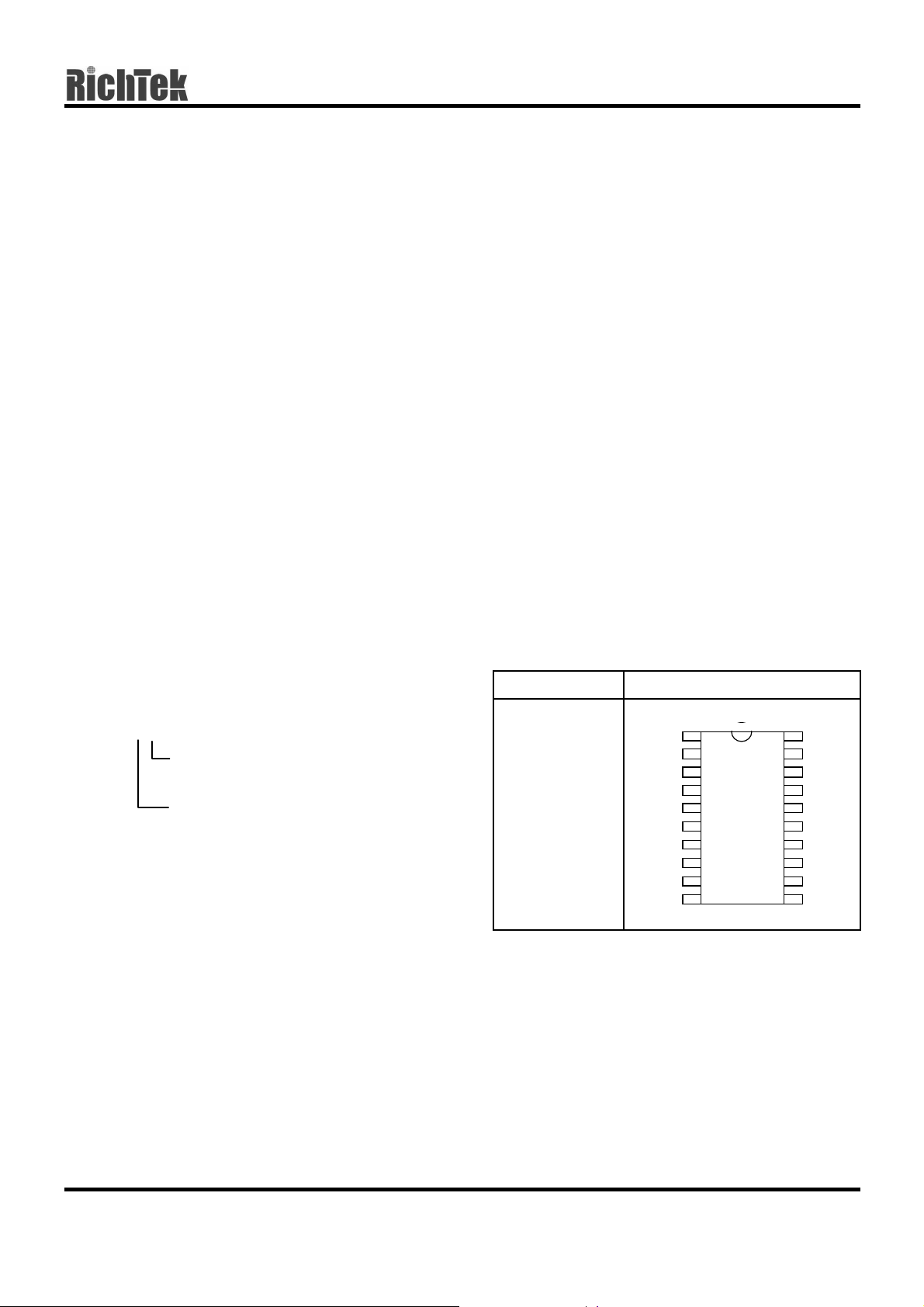
Pin Configurations
Part Number Pin Configurations
FB
TOP VIEW
1
2
3
4
5
6
7
8
9
10
20
19
18
17
16
15
14
13
12
11
NC
OVP
VCC
LGATE
PGND
BOOT
UGATE
PHASE
PGOOD
GND
RT9224CCS
(Plastic SOP-20)
VSEN
OCSET
SS
VID0
VID1
VID2
VID3
VID4
NC
DS9224C-01 May 2001 www.richtek-ic.com.tw
1
Page 2
RT9224C
Preliminary
Absolute Maximum Ratings
Supply Voltage +15V
z
Boot Voltage +15V
z
Input, Output or I/O Voltage GND – 0.3V to VCC + 0.3V
z
Storage Temperature Range –65°C ~150°C
z
Package Thermal Resistance
z
SOP-20, θ
JA
87°C/W
Recommended Operating Conditions
Supply Voltage +12V±10%
z
Ambient Temperature Range 0°C to 70°C
z
Junction Temperature Range 0°C to 125°C
z
Electrical Characteristics
(TA = 25°C, recommended operating conditions, unless otherwise specified)
Parameter Symbol Test Conditions Min Typ Max Units
VCC Supply Current
Nominal Supply
I
CC
UGATE and LGATE Open -- 3 -- mA
Power-On Reset
VCC Rising Threshold
VCC Falling Threshold
Rising V
OCSET
Threshold
V
OCSET
V
OCSET
= 4.5V
= 4.5V
-- 9.5 -- V
-- 7.5 -- V
-- 1.6 -- V
Oscillator
Free Running Frequency 170 200 230
Ramp Amplitude
∆V
OSC
-- 1.9 --
Reference and DAC
DAC (VID0 – VID4) Input Low Voltage -- -- 0.8
DAC (VID0 – VID4) Input High Voltage 2.0 -- --
DACOUT Voltage Accuracy -1.0 -- +1.0
Error Amplifier
DC Gain -- 65 --
Gate Drivers
UGATE Source
UGATE Sink
LGATE Source
LGATE Sink
R
UGATEVBOOT
R
UGATEVUGATE
I
LGATE
R
LGATEVLGATE
VCC = 12V, V
- V
- V
= 1V
PHASE
PHASE
LGATE
= 12V
= 1V
= 6V
-- 8 --
-- 5 --
-- 500 --
-- 5 --
To be continued
KHz
V
P-P
V
V
%
dB
Ω
Ω
mA
Ω
www.richtek-ic.com.tw DS9224C-01 May 2001
2
Page 3
Protection
Preliminary RT9224C
Parameter Symbol Test Conditions Min Typ Max Units
Over-voltage Trip (VSEN/DACOUT) -- 115 120
OCSET Current Source
OVP Sourcing Current
Soft-Start Current
I
OCSETVOCSET
I
OVP
I
SS
V
SEN
VSS = 1.5V
= 4.5V
= 5.5V, V
OVP
= 0V
167 200 233
60 -- --
-- 10 --
Power Good
Upper Threshold (VSEN/DACOUT) VSEN Rising 106 -- 114
Lower Threshold (VSEN/DACOUT) VSEN Falling 89 -- 96
Hysteresis (VSEN/DACOUT) Upper and Lower Threshold -- 2 --
PGOOD Voltage Low
V
PGOODIPGOOD
= -5mA
-- 0.5 --
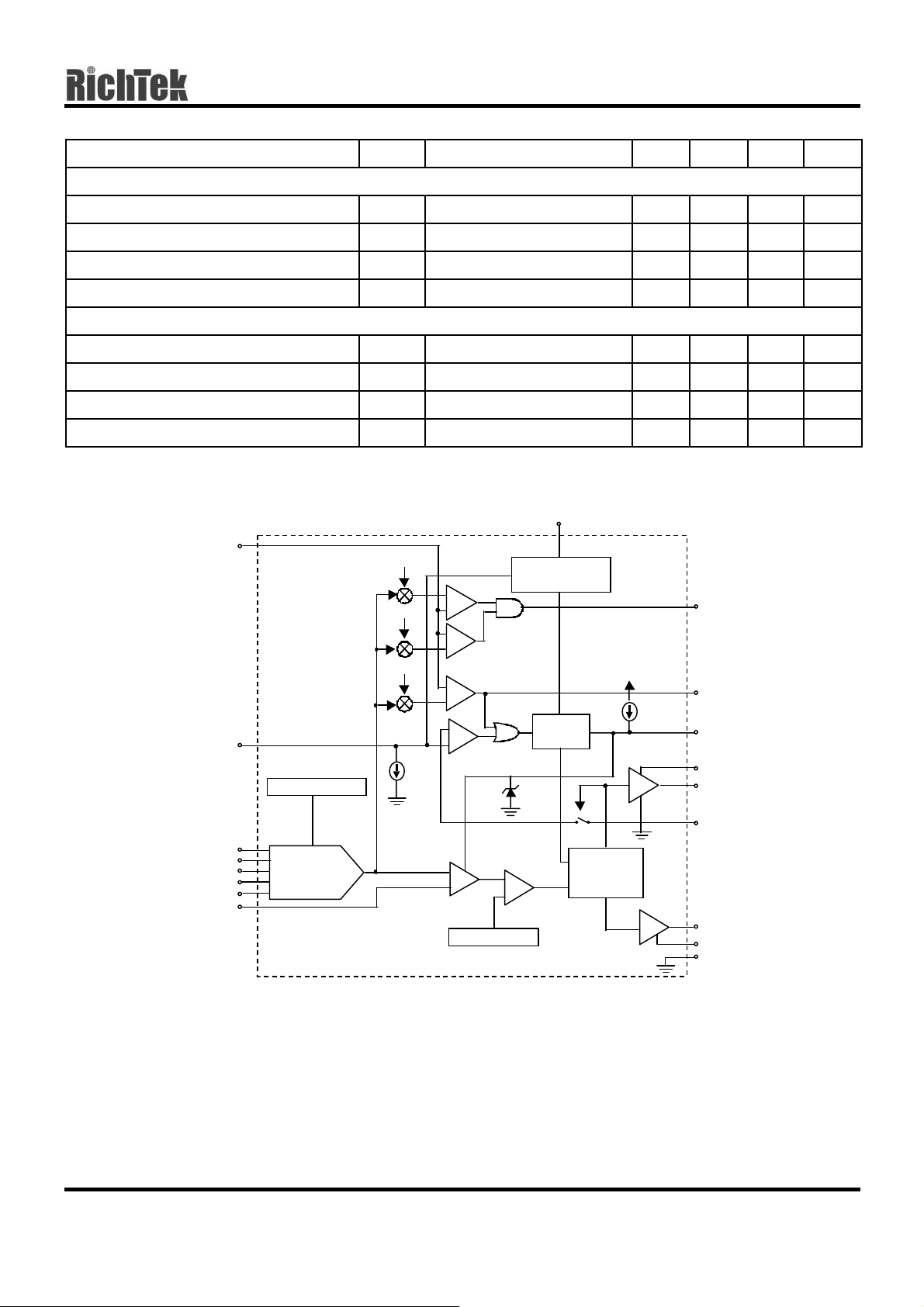
Function Block Diagram
VCC
VSEN
OCSET
REFE RENCE
110%
90%
115%
200µA
+
_
+
_
OVER-
VOLTAGE
+
_
+
_
OVER-
CURRENT
4. 5V
POWER-ON
RESET (POR)
SOFT-
START
PGOOD
OVP
10µA
SS
BOOT
UGATE
%
µA
mA
µA
%
%
%
V
PHASE
LG ATE
PGND
GND
_
INHIB IT
GATE
CONTROL
LO GIC
PWM
VID0
VID1
VID2
VID3
VID4
FB
DS9224C-01 May 2001 www.richtek-ic.com.tw
TTL D/A
CONVERTER
(DAC)
DACO UT
ERRO R
AMP
+
OSCILLATOR
PWM
COMPARATOR
+
_
3
Page 4

RT9224C
Preliminary
Pin Description
Pin No. Pin Name Pin Function
1VSEN
2 OCSET
3SS
4VID0
5VID1
6VID2
7VID3
8VID4
9NC
10 FB
11 GND
12 PGOOD
Output voltage monitoring input for OVP & PGOOD
Over current set pin, sinks 200µA through a resistor (R
MOSFET to set the trip point:
200µA × R
I
=
PEAK
An over-current trip cycles the soft-start function
Soft start speed is set by internal 10µA current source and capacitor from this pin to GND
Switching regulator output voltage setting
Switching regulator output voltage setting
Switching regulator output voltage setting
Switching regulator output voltage setting
Switching regulator output voltage setting
No connection
Feedback input pin
IC signal ground
Open drain logic output
This pin is pulled low when the converter output is not within ±10% of the DACOUT
reference voltage
MOSFET-on resistance
OCS
) from this pin to upper N-
OCS
13 PHASE
14 UGATE
15 BOOT
16 PGND
17 LGATE
18 VCC
19 OVP
20 NC No connection
Current limit sense input
High side driver output
Driver power
Low side driver GND
Low side driver output
Power supply input
Over voltage protection
This pin is pulled high when the VSEN voltage is over 15% of the DACOUT reference
voltage
www.richtek-ic.com.tw DS9224C-01 May 2001
4
Page 5

Preliminary
Table 1 Output Voltage Program
RT9224C
Pin Name
VID4 VID3 VID2 VID1 VID0
11111 1.075V
11110 1.100V
11101 1.125V
11100 1.150V
11011 1.175V
11010 1.200V
11001 1.225V
11000 1.250V
10111 1.275V
10110 1.300V
10101 1.325V
10100 1.350V
10011 1.375V
10010 1.400V
10001 1.425V
Nominal Output Voltage DACOUT
10000 1.450V
01111 1.475V
01110 1.500V
01101 1.525V
01100 1.550V
01011 1.575V
01010 1.600V
01001 1.625V
01000 1.650V
00111 1.675V
00110 1.700V
00101 1.725V
00100 1.750V
00011 1.775V
00010 1.800V
00001 1.825V
00000 1.850V
Note: (1) 0:Connected to GND (2) 1:Open
DS9224C-01 May 2001 www.richtek-ic.com.tw
5
Page 6

RT9224C
Typical Application Circuit
L1
VIN = 5V
F1
1µHC
IN
+
5×1000µF
Preliminary
2N63 94
2×1µF
+12V
0.1µF
0.1µF
VSEN
VID0
VID1
VID2
VID3
VID4
10
SS
Ω
15V
19
_
_
+
FB
10
18
3
1
4
5
6
7
8
MONI TOR AND
PROTECTION
OSC
D/A
+
2K
1000 pF
OVPVCC
11
OCSET
2
12
15
14
13
17
16
GND
PGOOD
BOOT
UGATE
PHASE
LGATE
PGND
1K
D2
Q2
Q1
L2 - 3µH
C
OUT
9×1000µF
4.99K
0.68µF
750K
+V
O
+
Component Selection Notes:
C
, C
– Each 1000µF 6.3WV DC, Sanyo MV-GX or Equivalent.
IN
OUT
L2 – Core: Micrometals T50-52B; Winding: 10 Turns of 16AWG.
L1 – Core: Micrometals T50-52; Winding: 5 Turns of 18AWG.
D2 – 3A, 40V Schottky, Motorola MBR340 or Equivalent.
Q1, Q2 – PHB83N03LT; PHB95N03LT
www.richtek-ic.com.tw DS9224C-01 May 2001
6
Page 7

Package Information
Preliminary
RT9224C
H
M
B
A
C
FD
Dimensions In Millimeters Dimensions In Inches
Symbol
Min Max Min Max
A 12.598 13.005 0.496 0.512
B 7.391 7.595 0.291 0.299
C 2.362 2.642 0.093 0.104
D 0.330 0.508 0.013 0.020
I
B
J
F 1.194 1.346 0.047 0.053
H 0.229 0.330 0.009 0.013
I 0.102 0.305 0.004 0.012
J 10.008 10.643 0.394 0.419
M 0.381 1.270
0.015 0.050
DS9224C-01 May 2001 www.richtek-ic.com.tw
7
Page 8

RT9224C
Preliminary
RICHTEK TECHNOLOGY CORP.
Headquarter
6F, No. 35, Hsintai Road, Chupei City
Hsinchu, Taiwan, R.O.C.
Tel: (8863)5510047 Fax: (8863)5537749
www.richtek-ic.com.tw
RICHTEK TECHNOLOGY CORP.
Taipei Office (Marketing)
8F-1, No. 137, Lane 235, Paochiao Road, Hsintien City
Taipei County, Taiwan, R.O.C.
Tel: (8862)89191466 Fax: (8862)89191465
Email: marketing@richtek-ic.com.tw
DS9224C-01 May 2001
8
 Loading...